
Nanostructured Semiconductors for Flexible Thermoelectric Applications


Abstract
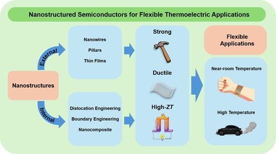
1. Introduction
2. Low-Dimensional TE Semiconductors
2.1. Nanowires
2.2. Pillars
2.3. Thin Films

3. Defect Engineering
3.1. Dislocation Engineering
3.2. Boundary Engineering

3.3. Nanocomposites
4. Flexible Thermoelectric Applications
4.1. Near-Room-Temperature Applications

4.2. High-Temperature Applications
5. Conclusions and Outlook
Author Contributions
Funding
Data Availability Statement
Conflicts of Interest
Abbreviations
| TE | Thermoelectric |
| TEM | Transmission electron microscopy |
| SEM | Scanning electron microscopy |
| STEM | Scanning transmission electron microscopy |
| 2D | Two-dimensional |
| 3D | Three-dimensional |
| TEG | Thermoelectric generator |
| SWCNT | Single-walled carbon nanotube |
References
- Li, G.; Aydemir, U.; Morozov, S.I.; Miller, S.A.; An, Q.; Goddard, W.A.; Zhai, P.; Zhang, Q.; Snyder, G.J. Mechanical properties in thermoelectric oxides: Ideal strength, deformation mechanism, and fracture toughness. Acta Mater. 2018, 149, 341–349. [Google Scholar] [CrossRef]
- Yun, J.S.; Choi, S.; Im, S.H. Advances in carbon-based thermoelectric materials for high-performance, flexible thermoelectric devices. Carbon Energy 2021, 3, 667–708. [Google Scholar] [CrossRef]
- Zhou, Y.; Zhao, L. Promising Thermoelectric Bulk Materials with 2D Structures. Adv. Mater. 2017, 29, 1702676. [Google Scholar] [CrossRef]
- Funahashi, R. Waste heat recovery using thermoelectric oxide materials. Sci. Adv. Mater. 2011, 3, 682–686. [Google Scholar] [CrossRef]
- Deng, W.; Li, G.; Zhang, X.; Morozov, S.I.; Goddard, W.A.; Zhai, P. The Mechanism of Deformation and Failure of In4Se3 Based Thermoelectric Materials. ACS Appl. Energy Mater. 2019, 3, 1054–1062. [Google Scholar] [CrossRef]
- Wu, L.; Lu, Z.; Feng, X.; Duan, B.; Wang, H.; Li, W.; Zhai, P.; Li, G.; Zhang, Q. Ultrahigh Tensile Ductility of Ag2Te Nanowire at Room Temperature. Adv. Funct. Mater. 2025, 35, 2423014. [Google Scholar] [CrossRef]
- Li, G.; An, Q.; Morozov, S.I.; Duan, B.; Goddard, W.A.; Zhang, Q.; Zhai, P.; Snyder, G.J. Ductile deformation mechanism in semiconductor α-Ag2S. NPJ Comput. Mater. 2018, 4, 44. [Google Scholar] [CrossRef]
- Li, G.; An, Q.; Duan, B.; Borgsmiller, L.; Al Malki, M.; Agne, M.; Aydemir, U.; Zhai, P.; Zhang, Q.; Morozov, S.I. Fracture toughness of thermoelectric materials. Mater. Sci. Eng. R Rep. 2021, 144, 100607. [Google Scholar] [CrossRef]
- Lu, Y.; Zhou, Y.; Wang, W.; Hu, M.; Huang, X.; Mao, D.; Huang, S.; Xie, L.; Lin, P.; Jiang, B.; et al. Staggered-layer-boosted flexible Bi2Te3 films with high thermoelectric performance. Nat. Nanotechnol. 2023, 18, 1281–1288. [Google Scholar] [CrossRef] [PubMed]
- Duan, B.; Li, Y.; Li, J.; Gao, Y.; Zhai, P.; Yang, J.; Lu, Z.; Yang, H.; Wang, H.; Li, G. Regulation of oxygen vacancy and reduction of lattice thermal conductivity in ZnO ceramic by high temperature and high pressure method. Ceram. Int. 2020, 46, 26176–26181. [Google Scholar] [CrossRef]
- Peng, J.; Snyder, G.J. A figure of merit for flexibility. Science 2019, 366, 690–691. [Google Scholar] [CrossRef] [PubMed]
- Liu, Q.; Jia, R.; Gao, X.; Huang, B.; Li, G.; Guo, Z. Micro-mechanism of the size effect on the deformation homogeneity of Sb2Te3 semiconductors. Dalton Trans. 2025, 54, 7272–7280. [Google Scholar] [CrossRef] [PubMed]
- Qiao, J.X.; Zhao, Y.; Jin, Q.; Tang, J.; Kang, S.Q.; Qiu, J.H.; Tai, K.P. Tailoring Nanoporous Structures in Bi2Te3 Thin Films for Improved Thermoelectric Performance. Acs Appl. Mater. Interfaces 2019, 11, 38075–38083. [Google Scholar] [CrossRef]
- Yang, H.; Huang, X.; Duan, B.; Wu, L.; Wang, H.; Feng, X.; Jiang, M.; Li, G.; Zhou, L.; Zhai, P.; et al. Dense dislocations induced ductile SnTe thermoelectric semiconductor over a wide range of temperatures. J. Mater. Sci. Technol. 2023, 144, 213–218. [Google Scholar] [CrossRef]
- Huang, M.; Zhai, P.; Li, G.; An, Q.; Morozov, S.I.; Li, W.; Zhang, Q.; Goddard, W.A. Nanotwin-induced ductile mechanism in thermoelectric semiconductor PbTe. Matter 2022, 5, 1839–1852. [Google Scholar] [CrossRef]
- Li, G.; Aydemir, U.; Morozov, S.I.; Wood, M.; An, Q.; Zhai, P.; Zhang, Q.; Goddard, W.A.; Snyder, G.J. Superstrengthening Bi2Te3 through Nanotwinning. Phys. Rev. Lett. 2017, 119, 085501. [Google Scholar] [CrossRef]
- Huang, X.; Feng, X.; An, Q.; Huang, B.; Zhang, X.; Lu, Z.; Li, G.; Zhai, P.; Duan, B.; Snyder, G.J.; et al. Stacking fault-induced strengthening mechanism in thermoelectric semiconductor Bi2Te3. Matter 2023, 6, 3087–3098. [Google Scholar] [CrossRef]
- Wu, Y.; Zhang, Y.; Wang, X.; Hu, W.; Zhao, S.; Officer, T.; Luo, K.; Tong, K.; Du, C.; Zhang, L.; et al. Twisted-layer boron nitride ceramic with high deformability and strength. Nature 2024, 626, 779–784. [Google Scholar] [CrossRef]
- Deng, T.; Gao, Z.; Li, Z.; Qiu, P.; Li, Z.; Yuan, X.; Ming, C.; Wei, T.-R.; Chen, L.; Shi, X. Room-temperature exceptional plasticity in defective Bi2Te3-based bulk thermoelectric crystals. Science 2024, 386, 1112–1117. [Google Scholar] [CrossRef]
- Yang, H.; Wu, L.; Feng, X.; Wang, H.; Huang, X.; Duan, B.; Li, G.; Zhai, P.; Zhang, Q. Optimization of Mechanical and Thermoelectric Properties of SnTe—Based Semiconductors by Mn Alloying Modulated Precipitation Evolution. Small 2024, 20, e2310692. [Google Scholar] [CrossRef]
- Yang, H.; Wu, L.; Feng, X.; Huang, X.; Wang, H.; Duan, B.; Li, G.; Zhai, P.; Zhang, Q. Constructing Coated Grain Nanocomposites and Intracrystalline Precipitates to Simultaneously Improve the Thermoelectric and Mechanical Properties of SnTe by MgB2 and Sb Co—Doping. Adv. Funct. Mater. 2024, 34, 2316344. [Google Scholar] [CrossRef]
- Xiao, C.; Wu, L.; Fang, K.; Xia, Z.; Jiang, N.; Duan, B.; Feng, X.; Zhou, L.; Zhai, P.; Li, G.; et al. Simultaneous enhancement of strength and ductility of Cu2-Se through dual-phase heterostructure. Acta Mater. 2025, 286, 120761. [Google Scholar] [CrossRef]
- Zhao, P.; Yu, F.; Wang, B.; Zhao, H.; Chen, C.; Wang, D.; Ying, P.; Wu, Y.; Li, P.; Zhang, B.; et al. Porous bismuth antimony telluride alloys with excellent thermoelectric and mechanical properties. J. Mater. Chem. A 2021, 9, 4990–4999. [Google Scholar] [CrossRef]
- Jin, D.; Ruan, Z.; Duan, B.; Li, J.; Zhai, P.; Yang, H.; Wang, H.; Li, G.; Zhou, L. Rapid preparation of high-performance S0.4Co4Sb11.2Te0.8 skutterudites with a highly porous structure. J. Eur. Ceram. Soc. 2021, 41, 4484–4489. [Google Scholar] [CrossRef]
- Yang, H.; Duan, B.; Zhou, L.; Li, J.; Wang, H.; Xiao, C.; Li, G.; Zhai, P. Rapid fabrication and thermoelectric properties of Sn1.03Te-based materials with porous configuration. J. Mater. Sci. Mater. Electron. 2022, 33, 2479–2489. [Google Scholar] [CrossRef]
- Elyamny, S.; Dimaggio, E.; Magagna, S.; Narducci, D.; Pennelli, G. High Power Thermoelectric Generator Based on Vertical Silicon Nanowires. Nano Lett. 2020, 20, 4748–4753. [Google Scholar] [CrossRef] [PubMed]
- Lu, Y.; Qiu, Y.; Cai, K.; Li, X.; Gao, M.; Jiang, C.; He, J. Ultrahigh performance PEDOT/Ag2Se/CuAgSe composite film for wearable thermoelectric power generators. Mater. Today Phys. 2020, 14, 100223. [Google Scholar] [CrossRef]
- Liang, J.; Wang, T.; Qiu, P.; Yang, S.; Ming, C.; Chen, H.; Song, Q.; Zhao, K.; Wei, T.-R.; Ren, D.; et al. Flexible thermoelectrics: From silver chalcogenides to full-inorganic devices. Energy Environ. Sci. 2019, 12, 2983–2990. [Google Scholar] [CrossRef]
- Wu, D.; Zhu, Y.; Huang, M.; Zhao, L.; Li, Z. Molecular dynamics study on shock-induced spallation and damage evolution in nano-polycrystalline Ta: Internal grain size effect vs external shock intensity effect. J. Appl. Phys. 2021, 130, 205104. [Google Scholar] [CrossRef]
- Su, D.; Liedienov, N.A.; Kalita, V.M.; Fesych, I.V.; Xu, W.; Bodnaruk, A.V.; Dzhezherya, Y.I.; Li, Q.; Liu, B.; Levchenko, G.G. Structural size effect-, aging time-, and pressure-dependent functional properties of Mn-containing perovskite nanoparticles. Acta Mater. 2024, 280, 120332. [Google Scholar] [CrossRef]
- Chen, M.; Pethö, L.; Sologubenko, A.; Ma, H.; Michler, J.; Spolenak, R.; Wheeler, J. Achieving micron-scale plasticity and theoretical strength in Silicon. Nat. Commun. 2020, 11, 2681. [Google Scholar] [CrossRef] [PubMed]
- Wang, Y.-B.; Wang, L.-F.; Joyce, H.J.; Gao, Q.; Liao, X.-Z.; Mai, Y.-W.; Tan, H.H.; Zou, J.; Ringer, S.P.; Gao, H.-J.; et al. Super Deformability and Young’s Modulus of GaAs Nanowires. Adv. Mater. 2011, 23, 1356–1360. [Google Scholar] [CrossRef]
- Kashyap, A.; Rawat, D.; Sarkar, D.; Singh, N.; Biswas, K.; Soni, A. Chemically Transformed Ag2Te Nanowires on Polyvinylidene Fluoride Membrane For Flexible Thermoelectric Applications. Angew. Chem. Int. Ed. 2024, 63, e202401234. [Google Scholar] [CrossRef]
- Hochbaum, A.I.; Chen, R.; Delgado, R.D.; Liang, W.; Garnett, E.C.; Najarian, M.; Majumdar, A.; Yang, P. Enhanced thermoelectric performance of rough silicon nanowires. Nature 2008, 451, 163–167. [Google Scholar] [CrossRef]
- Fonseca, L.; Donmez-Noyan, I.; Dolcet, M.; Estrada-Wiese, D.; Santander, J.; Salleras, M.; Gadea, G.; Pacios, M.; Sojo, J.-M.; Morata, A.; et al. Transitioning from Si to SiGe Nanowires as Thermoelectric Material in Silicon-Based Microgenerators. Nanomaterials 2021, 11, 517. [Google Scholar] [CrossRef]
- Boukai, A.I.; Bunimovich, Y.; Tahir-Kheli, J.; Yu, J.-K.; Goddard Iii, W.A.; Heath, J.R. Silicon nanowires as efficient thermoelectric materials. Nature 2008, 451, 168–171. [Google Scholar] [CrossRef]
- Tian, Y.; Sakr, M.R.; Kinder, J.M.; Liang, D.; MacDonald, M.J.; Qiu, R.L.J.; Gao, H.-J.; Gao, X.P.A. One-Dimensional Quantum Confinement Effect Modulated Thermoelectric Properties in InAs Nanowires. Nano Lett. 2012, 12, 6492–6497. [Google Scholar] [CrossRef]
- Gong, Q.; Wu, L.; Lei, Z.; Huang, X.; Qiu, L.; Sheng, L.; Lu, Z.; Feng, X.; Li, G. Synergistic enhancement of strength and plasticity in SnSe via size-effect-triggered multiple slip activation. Ceram. Int. 2025, 51, 47763–47770. [Google Scholar] [CrossRef]
- Liu, S.; Hu, B.; Liu, D.; Li, F.; Li, J.-F.; Li, B.; Li, L.; Lin, Y.-H.; Nan, C.-W. Micro-thermoelectric generators based on through glass pillars with high output voltage enabled by large temperature difference. Appl. Energy 2018, 225, 600–610. [Google Scholar] [CrossRef]
- Yue, Y.; Lyu, W.; Liu, W.-D.; Shi, X.-L.; Moshwan, R.; Wang, N.; Li, M.; Zhang, C.; Chen, Z.-G. Solvothermal synthesis of micro-pillar shaped Ag2Se and its thermoelectric potential. Mater. Today Chem. 2024, 39, 102183. [Google Scholar] [CrossRef]
- Zheng, Z.-H.; Shi, X.-L.; Ao, D.-W.; Liu, W.-D.; Li, M.; Kou, L.-Z.; Chen, Y.-X.; Li, F.; Wei, M.; Liang, G.-X.; et al. Harvesting waste heat with flexible Bi2Te3 thermoelectric thin film. Nat. Sustain. 2022, 6, 180–191. [Google Scholar] [CrossRef]
- Shang, H.; Li, T.; Luo, D.; Yu, L.; Zou, Q.; Huang, D.; Xiao, L.; Gu, H.; Ren, Z.; Ding, F. High-Performance Ag-Modified Bi0.5Sb1.5Te3 Films for the Flexible Thermoelectric Generator. ACS Appl. Mater. Interfaces 2020, 12, 7358–7365. [Google Scholar] [CrossRef]
- Cao, T.; Shi, X.-L.; Hu, B.; Liu, S.; Lyu, W.; Li, M.; Wang, S.; Chen, W.; Liu, W.-D.; Moshwan, R.; et al. Indium-Doping Advances High-Performance Flexible Ag2Se Thin Films. Adv. Sci. 2025, 12, e2500364. [Google Scholar] [CrossRef] [PubMed]
- Yang, D.; Zhang, D.; Ao, D.; Nisar, M.; Mansoor, A.; Chen, Y.; Li, F.; Ma, H.; Liang, G.; Zhang, X.; et al. High thermoelectric performance of aluminum-doped cuprous selenide thin films with exceptional flexibility for wearable applications. Nano Energy 2023, 117, 108930. [Google Scholar] [CrossRef]
- Li, D.; Shi, X.-L.; Zhu, J.; Cao, T.; Ma, X.; Li, M.; Han, Z.; Feng, Z.; Chen, Y.; Wang, J.; et al. High-performance flexible p-type Ce-filled Fe3CoSb12 skutterudite thin film for medium-to-high-temperature applications. Nat. Commun. 2024, 15, 4242. [Google Scholar] [CrossRef] [PubMed]
- Shi, X.; Chen, H.; Hao, F.; Liu, R.; Wang, T.; Qiu, P.; Burkhardt, U.; Grin, Y.; Chen, L. Room-temperature ductile inorganic semiconductor. Nat. Mater. 2018, 17, 421–426. [Google Scholar] [CrossRef] [PubMed]
- Ding, Y.; Huang, X.; Feng, X.; Wu, L.; Li, Z.; Niu, G.; Zhang, Z.; Duan, B.; Zhai, P.; Li, G.; et al. Boundary Engineering-Induced Strong Yet Ductile Bi2Te3 Thin Film with High Thermoelectric Performance. Adv. Funct. Mater. 2025, e17343. [Google Scholar] [CrossRef]
- Rasmi, T.; Chandra Bose, R.S.; Varun, T.S.; Arya, P.; Srikanth, P.; Haripriya, V.K.; Malini, K.A. Enhanced thermoelectric performance of n-type Bi2Te3 thin films via thermal evaporation and optimized post-annealing. J. Alloys Compd. 2025, 1034, 181378. [Google Scholar] [CrossRef]
- Chen, W.; Li, M.; Wang, X.; Otte, J.; Zhang, M.; Zhang, C.; Cao, T.; Hu, B.; Li, N.; Liu, W.-D.; et al. Flexible Ag2Se-based thin-film thermoelectrics for sustainable energy harvesting and cooling. Nat. Commun. 2025, 16, 7579. [Google Scholar] [CrossRef]
- Yonenaga, I. Hardness, Yield Strength, and Dislocation Velocity in Elemental and Compound Semiconductors. Mater. Trans. 2005, 46, 1979–1985. [Google Scholar] [CrossRef]
- Jiang, Q.; Hu, H.; Yang, J.; Xin, J.; Li, S.; Viola, G.; Yan, H. High Thermoelectric Performance in SnTe Nanocomposites with All-Scale Hierarchical Structures. Acs Appl. Mater. Interfaces 2020, 12, 23102–23109. [Google Scholar] [CrossRef]
- Yin, Z.; Zhang, H.; Wang, Y.; Wu, Y.; Xing, Y.; Wang, X.; Fang, X.; Yu, Y.; Guo, X. Ultrahigh-Pressure Structural Modification in BiCuSeO Ceramics: Dense Dislocations and Exceptional Thermoelectric Performance. Adv. Energy Mater. 2025, 15, 2403174. [Google Scholar] [CrossRef]
- Xu, L.; Xiao, Y.; Wang, S.; Cui, B.; Wu, D.; Ding, X.; Zhao, L. Dense dislocations enable high-performance PbSe thermoelectric at low-medium temperatures. Nat. Commun. 2022, 13, 6449. [Google Scholar] [CrossRef] [PubMed]
- Lee, J.; Kim, J.; Moon, W.; Berger, A.; Lee, J. Enhanced Seebeck Coefficients of Thermoelectric Bi2Te3 Nanowires as a Result of an Optimized Annealing Process. J. Phys. Chem. C 2012, 116, 19512–19516. [Google Scholar] [CrossRef]
- Zhang, F.; Zhu, L.; Song, M.; Cao, X.; Pang, X.; Liang, P.; Peng, Z.; Chao, X.; Yang, Z.; Wu, D. Giant Deformation Induced Staggered-Layer Structure Promoting the Thermoelectric and Mechanical Performance in n-Type Bi2(Te,Se)3. Small 2024, 20, 2401070. [Google Scholar] [CrossRef] [PubMed]
- Huang, B.; Li, G.; Duan, B.; Li, W.; Zhai, P.; Goddard, W.A. Order-Tuned Deformability of Bismuth Telluride Semiconductors: An Energy-Dissipation Strategy for Large Fracture Strain. ACS Appl. Mater. Interfaces 2021, 13, 57629–57637. [Google Scholar] [CrossRef]
- Huang, B.; Li, G.; Xiao, C.; Duan, B.; Li, W.; Zhai, P.; Goddard, W.A. Compression Induced Deformation Twinning Evolution in Liquid-Like Cu2Se. ACS Appl. Mater. Interfaces 2022, 14, 18671–18681. [Google Scholar] [CrossRef]
- Li, W.; Zhang, X.; Duan, B.; Huang, B.; Huang, M.; Li, G.; Zhai, P. Size effect on mechanical properties of nanotwinned Mg2Si from molecular dynamics simulation. Comput. Mater. Sci. 2020, 185, 109972. [Google Scholar] [CrossRef]
- Lu, Z.; Zhai, P.; Ran, Y.; Li, W.; Zhang, X.; Li, G. Enhancement of mechanical properties of InSb through twin boundary engineering. Scr. Mater. 2022, 215, 114734. [Google Scholar] [CrossRef]
- Wang, H.; Feng, X.; Lu, Z.; Duan, B.; Yang, H.; Wu, L.; Zhou, L.; Zhai, P.; Snyder, G.J.; Li, G.; et al. Synergetic Enhancement of Strength–Ductility and Thermoelectric Properties of Ag2Te by Domain Boundaries. Adv. Mater. 2023, 35, 2302969. [Google Scholar] [CrossRef]
- Liang, Q.; Yang, D.; Xia, F.; Bai, H.; Peng, H.; Yu, R.; Yan, Y.; He, D.; Cao, S.; Van Tendeloo, G.; et al. Phase-Transformation-Induced Giant Deformation in Thermoelectric Ag2Se Semiconductor. Adv. Funct. Mater. 2021, 31, 2106938. [Google Scholar] [CrossRef]
- Lu, Z.; Huang, B.; Li, G.; Zhang, X.; An, Q.; Duan, B.; Zhai, P.; Zhang, Q.; Goddard, W.A. Shear induced deformation twinning evolution in thermoelectric InSb. NPJ Comput. Mater. 2021, 7, 111. [Google Scholar] [CrossRef]
- Huang, X.; Zhou, X.; Wu, L.; Feng, X.; Zhai, P.; Duan, B.; Li, G.; Zhang, Q.; Goddard, W.A. A nanotwin-based physical model for designing robust layered bismuth telluride thermoelectric semiconductor. Cell Rep. Phys. Sci. 2024, 5, 101841. [Google Scholar] [CrossRef]
- Li, G.; He, J.; An, Q.; Morozov, S.I.; Hao, S.; Zhai, P.; Zhang, Q.; Goddard, W.A.; Snyder, G.J. Dramatically reduced lattice thermal conductivity of Mg2Si thermoelectric material from nanotwinning. Acta Mater. 2019, 169, 9–14. [Google Scholar] [CrossRef]
- Li, G.; An, Q.; Morozov, S.I.; Duan, B.; Goddard, W.A.; Zhai, P.; Zhang, Q.; Jeffrey Snyder, G. Mechanical softening of thermoelectric semiconductor Mg2Si from nanotwinning. Scr. Mater. 2018, 157, 90–94. [Google Scholar] [CrossRef]
- Wang, H.; Ma, H.; Duan, B.; Geng, H.; Zhou, L.; Li, J.; Zhang, X.; Yang, H.; Li, G.; Zhai, P. High-Pressure Rapid Preparation of High-Performance Binary Silver Sulfide Thermoelectric Materials. ACS Appl. Energy Mater. 2021, 4, 1610–1618. [Google Scholar] [CrossRef]
- Gayner, C.; Amouyal, Y. Energy Filtering of Charge Carriers: Current Trends, Challenges, and Prospects for Thermoelectric Materials. Adv. Funct. Mater. 2019, 30, 1901789. [Google Scholar] [CrossRef]
- Pakdel, A.; Guo, Q.; Nicolosi, V.; Mori, T. Enhanced thermoelectric performance of Bi–Sb–Te/Sb2O3 nanocomposites by energy filtering effect. J. Mater. Chem. A 2018, 6, 21341–21349. [Google Scholar] [CrossRef]
- Chen, T.; Liang, R.; Li, Y.; Zhou, Z.; Dong, X. Structure and electrical properties of perovskite layer (1−x)Sr2Nb2O7-x(Na0.5Bi0.5)TiO3 high-temperature piezoceramics. J. Am. Ceram. Soc. 2016, 100, 1065–1072. [Google Scholar] [CrossRef]
- Hong, T.; Guo, C.; Wang, D.; Qin, B.; Chang, C.; Gao, X.; Zhao, L.-D. Enhanced thermoelectric performance in SnTe due to the energy filtering effect introduced by Bi2O3. Mater. Today Energy 2022, 25, 100985. [Google Scholar] [CrossRef]
- Deng, Y.; Wei, M.; Lei, Y.; Lu, J.; Peng, P.; Zhang, Y.; Zheng, Z. Advances in silver-based chalcogenide flexible thermoelectric materials. CrystEngComm 2025, 27, 1055–1077. [Google Scholar] [CrossRef]
- Shi, Y.; Wang, Y.; Mei, D.; Chen, Z. Wearable Thermoelectric Generator With Copper Foam as the Heat Sink for Body Heat Harvesting. IEEE Access 2018, 6, 43602–43611. [Google Scholar] [CrossRef]
- Caballero-Calero, O.; Cervino-Solana, P.; Cloetens, P.; Monaco, F.; Martin-Gonzalez, M. Flexible polyester-embedded thermoelectric device with Bi2Te3 and Te legs for wearable power generation. Appl. Mater. Today 2024, 41, 102458. [Google Scholar] [CrossRef]
- Park, G.M.; Lee, S.; Hong, J.; Nahm, S.; Baek, S.H.; Kim, J.S.; Lee, S.Y.; Kim, S.K. Nanowire-Bundled Grain Boundaries in Thermoelectric Materials. Small 2025, 21, e2503539. [Google Scholar] [CrossRef]
- Cui, G.-P.; Feng, C.-P.; Xu, S.-C.; Sun, K.-Y.; Ji, J.-C.; Hou, L.; Lan, H.-B.; Shang, H.-J.; Ding, F.-Z. 3D-printed Bi2Te3-based Thermoelectric Generators for Energy Harvesting and Temperature Response. ACS Appl. Mater. Interfaces 2024, 16, 35353–35360. [Google Scholar] [CrossRef]
- Liu, K.; Tang, X.; Liu, Y.; Xu, Z.; Yuan, Z.; Zhang, Z. Enhancing the performance of fully-scaled structure-adjustable 3D thermoelectric devices based on cold–press sintering and molding. Energy 2020, 206, 118096. [Google Scholar] [CrossRef]
- Yang, S.E.; Lee, J.; Li, H.; Ryu, B.; Son, J.S. Design principles for 3D thermoelectric materials in power generators. Energy Environ. Sci. 2025, 18, 8537–8548. [Google Scholar] [CrossRef]
- Ren, W.; Sun, Y.; Zhao, D.; Aili, A.; Zhang, S.; Shi, C.; Zhang, J.; Geng, H.; Zhang, J.; Zhang, L.; et al. High-performance wearable thermoelectric generator with self-healing, recycling, and Lego-like reconfiguring capabilities. Sci. Adv. 2021, 7, eabe0586. [Google Scholar] [CrossRef]
- Lee, B.; Cho, H.; Park, K.T.; Kim, J.-S.; Park, M.; Kim, H.; Hong, Y.; Chung, S. High-performance compliant thermoelectric generators with magnetically self-assembled soft heat conductors for self-powered wearable electronics. Nat. Commun. 2020, 11, 5948. [Google Scholar] [CrossRef]
- Jing, Y.; Luo, J.; Han, X.; Yang, J.; Liu, Q.; Zheng, Y.; Chen, X.; Huang, F.; Chen, J.; Zhuang, Q.; et al. Scalable manufacturing of a durable, tailorable, and recyclable multifunctional woven thermoelectric textile system. Energy Environ. Sci. 2023, 16, 4334–4344. [Google Scholar] [CrossRef]
- Xu, H.; Zha, Z.; Li, F.; Liang, G.; Luo, J.; Zheng, Z.; Chen, Y.X. Optimization of Thermoelectric Performance of Ag2Te Films via a Co-Sputtering Method. Nanomaterials 2024, 14, 1762. [Google Scholar] [CrossRef]
- Liu, Y.M.; Shi, X.L.; Wu, T.; Wu, H.; Mao, Y.; Cao, T.; Wang, D.Z.; Liu, W.D.; Li, M.; Liu, Q.; et al. Boosting thermoelectric performance of single-walled carbon nanotubes-based films through rational triple treatments. Nat. Commun. 2024, 15, 3426. [Google Scholar] [CrossRef]
- Li, M.; Xiong, Y.; Wei, H.; Yao, F.; Han, Y.; Du, Y.; Xu, D. Flexible Te/PEDOT:PSS thin films with high thermoelectric power factor and their application as flexible temperature sensors. Nanoscale 2023, 15, 11237–11246. [Google Scholar] [CrossRef]
- Burton, M.R.; Mehraban, S.; Beynon, D.; McGettrick, J.; Watson, T.; Lavery, N.P.; Carnie, M.J. 3D Printed SnSe Thermoelectric Generators with High Figure of Merit. Adv. Energy Mater. 2019, 9, 1900201. [Google Scholar] [CrossRef]
- Karthikeyan, V.; Surjadi, J.U.; Li, X.; Fan, R.; Theja, V.C.S.; Li, W.J.; Lu, Y.; Roy, V.A.L. Three dimensional architected thermoelectric devices with high toughness and power conversion efficiency. Nat. Commun. 2023, 14, 2069. [Google Scholar] [CrossRef] [PubMed]
- Ding, Z.; Li, G.; Wang, Y.; Du, C.; Ye, Z.; Liang, L.; Tang, L.-C.; Chen, G. Ultrafast Response and Threshold Adjustable Intelligent Thermoelectric Systems for Next-Generation Self-Powered Remote IoT Fire Warning. Nano-Micro Lett. 2024, 16, 242. [Google Scholar] [CrossRef]
- Karthik, H.J.; Bhattacharyya, S. High-performance one-dimensional thermoelectric materials: Polyyne chains and their derivatives. Nanoscale Adv. 2025, 7, 4381–4396. [Google Scholar] [CrossRef]
- Frobenius, F.; Gaiser, G.; Rusche, U.; Weller, B. Thermoelectric Generators for the Integration into Automotive Exhaust Systems for Passenger Cars and Commercial Vehicles. J. Electron. Mater. 2015, 45, 1433–1440. [Google Scholar] [CrossRef]
- Kuroki, T.; Kabeya, K.; Makino, K.; Kajihara, T.; Kaibe, H.; Hachiuma, H.; Matsuno, H.; Fujibayashi, A. Thermoelectric Generation Using Waste Heat in Steel Works. J. Electron. Mater. 2014, 43, 2405–2410. [Google Scholar] [CrossRef]
- Feng, J.; Zhu, W.; Deng, Y.; Song, Q.; Zhang, Q. Enhanced Antioxidation and Thermoelectric Properties of the Flexible Screen-Printed Bi2Te3 Films through Interface Modification. ACS Appl. Energy Mater. 2019, 2, 2828–2836. [Google Scholar] [CrossRef]
- Somdock, N.; Harnwunggmoung, A.; Sakulkalavek, A.; Sakdanuphab, R. Effect of real working environment/formation of oxide phase on thermoelectric properties of flexible Sb2Te3 films. Ceram. Int. 2019, 45, 15860–15865. [Google Scholar] [CrossRef]
- Kim, S.; Mo, J.-H.; Jang, K.-S. High-Performance n-Type Carbon Nanotubes Doped by Oxidation of Neighboring Sb2Te3 for a Flexible Thermoelectric Generator. ACS Appl. Mater. Interfaces 2020, 12, 43778–43784. [Google Scholar] [CrossRef]
- Truong, D.C.; Thaowonkaew, S.; Muthitamongkol, P.; Horprathum, M.; Kumar, M.; Le, T.B.N.; Pham, A.T.T.; Seetawan, T.; Vora-ud, A.; Phan, T.B. Relaxation of residual stress-controlled thermopower factor in transparent-flexible Ti-doped ZnO thin films. Ceram. Int. 2022, 48, 2605–2613. [Google Scholar] [CrossRef]
- Norimasa, O.; Chiba, T.; Hase, M.; Komori, T.; Takashiri, M. Improvement of thermoelectric properties of flexible Bi2Te3 thin films in bent states during sputtering deposition and post-thermal annealing. J. Alloys Compd. 2022, 898, 162889. [Google Scholar] [CrossRef]


| Materials | Configuration | Dimension | Loading Mode | Mechanical Properties | T (K) | PF (μW cm−1 K−2) | ZT |
|---|---|---|---|---|---|---|---|
| Ag2Te [6] | Nanowire | 330 nm (Diameter) × 740 nm (Length) | Tension | 75.7% (Fracture Strain) | / | / | / |
| Ag2Te [33] | Nanowire | 50–100 nm (Diameter) | Tension | ~11.3 MPa (Tensile Strength) | 300 | 3.62 | 0.25 |
| Si [36] | Nanowire | 20 nm (Diameter) × 20 nm (Length) | / | / | 200 | / | 1.0 |
| SiGe [35] | Nanowire | 64 ± 11 nm (Diameter) | / | / | / | / | / |
| SnSe [38] | Pillar | 600 nm (Diameter) | Compression | 1.15 GPa (Yield Strengh) 7.3% (Strain) | / | / | / |
| Si [31] | Pillar | 1000 nm (Diameter) | Compression | 10.8 GPa (Engineering Stress) 10% (Strain) | / | / | / |
| Bi2Te3 [47] | Thin films | 1500 nm (Thickness) | Bending | 10,000 cycles (r = 4 mm) | 550 | 27.6 | / |
| Bi2Te3 [9] | Thin films | 12,000 mm (Thickness) | Bending | >1000 cycles (r = 5 mm) | 300 | 46 | 0.9 |
| Ag2Se [49] | Thin films | 15,000 mm (Thickness) | Bending | >1000 cycles (r = 5 mm) | 303 | 25.7 | 1.06 |
| Ag-Bi2Te3 [41] | Thin films | 468.9 nm (Thickness) | Bending | 2000 cycles (r = 18 mm) | 300 | 20.6 | 1.2 |
| Ag-Bi0.5Sb1.5Te3 [42] | Thin films | 750 nm (Thickness) | Bending | 1000 cycles (r = 5 mm) | 420 | 14.0 | / |
| Ag2Se [43] | Thin films | 200 nm (Thickness) | Bending | 500 cycles (r = 5 mm) | 300 | 26.3 | 1.0 |
| Cu2Se [44] | Thin films | 500 nm (Thickness) | Bending | 1000 cycles (r = 5 mm) | 548 | 19.2 | 0.76 |
| Ce-Fe3CoSb12 [45] | Thin films | 300 nm (Thickness) | Bending | 2000 cycles (r = 5 mm) | 653 | 10 | 0.6 |
Disclaimer/Publisher’s Note: The statements, opinions and data contained in all publications are solely those of the individual author(s) and contributor(s) and not of MDPI and/or the editor(s). MDPI and/or the editor(s) disclaim responsibility for any injury to people or property resulting from any ideas, methods, instructions or products referred to in the content. |
© 2025 by the authors. Licensee MDPI, Basel, Switzerland. This article is an open access article distributed under the terms and conditions of the Creative Commons Attribution (CC BY) license (https://creativecommons.org/licenses/by/4.0/).
Share and Cite
Luo, Y.; Yu, C.; Niu, Y.; Guo, H.; Feng, X. Nanostructured Semiconductors for Flexible Thermoelectric Applications. Nanomaterials 2025, 15, 1843. https://doi.org/10.3390/nano15241843
Luo Y, Yu C, Niu Y, Guo H, Feng X. Nanostructured Semiconductors for Flexible Thermoelectric Applications. Nanomaterials. 2025; 15(24):1843. https://doi.org/10.3390/nano15241843
Chicago/Turabian StyleLuo, Yi, Chengxuan Yu, Yuanbin Niu, Haoyi Guo, and Xiaobin Feng. 2025. "Nanostructured Semiconductors for Flexible Thermoelectric Applications" Nanomaterials 15, no. 24: 1843. https://doi.org/10.3390/nano15241843
APA StyleLuo, Y., Yu, C., Niu, Y., Guo, H., & Feng, X. (2025). Nanostructured Semiconductors for Flexible Thermoelectric Applications. Nanomaterials, 15(24), 1843. https://doi.org/10.3390/nano15241843