
Spin-Orbit-Coupling-Governed Optical Absorption in Bilayer MoS2 via Strain, Twist, and Electric Field Engineering


Abstract
1. Introduction
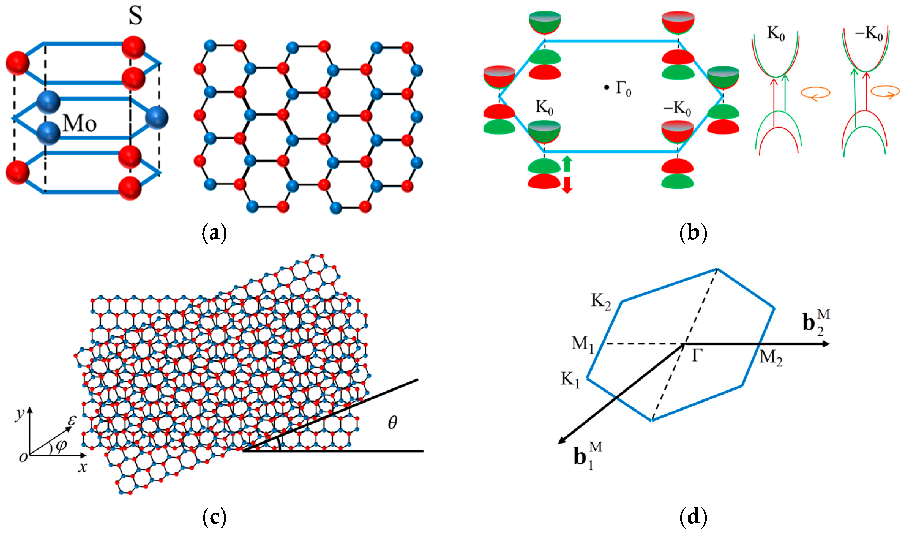
2. Theory
3. Results and Discussion
3.1. Band Structure Modulation Mechanisms
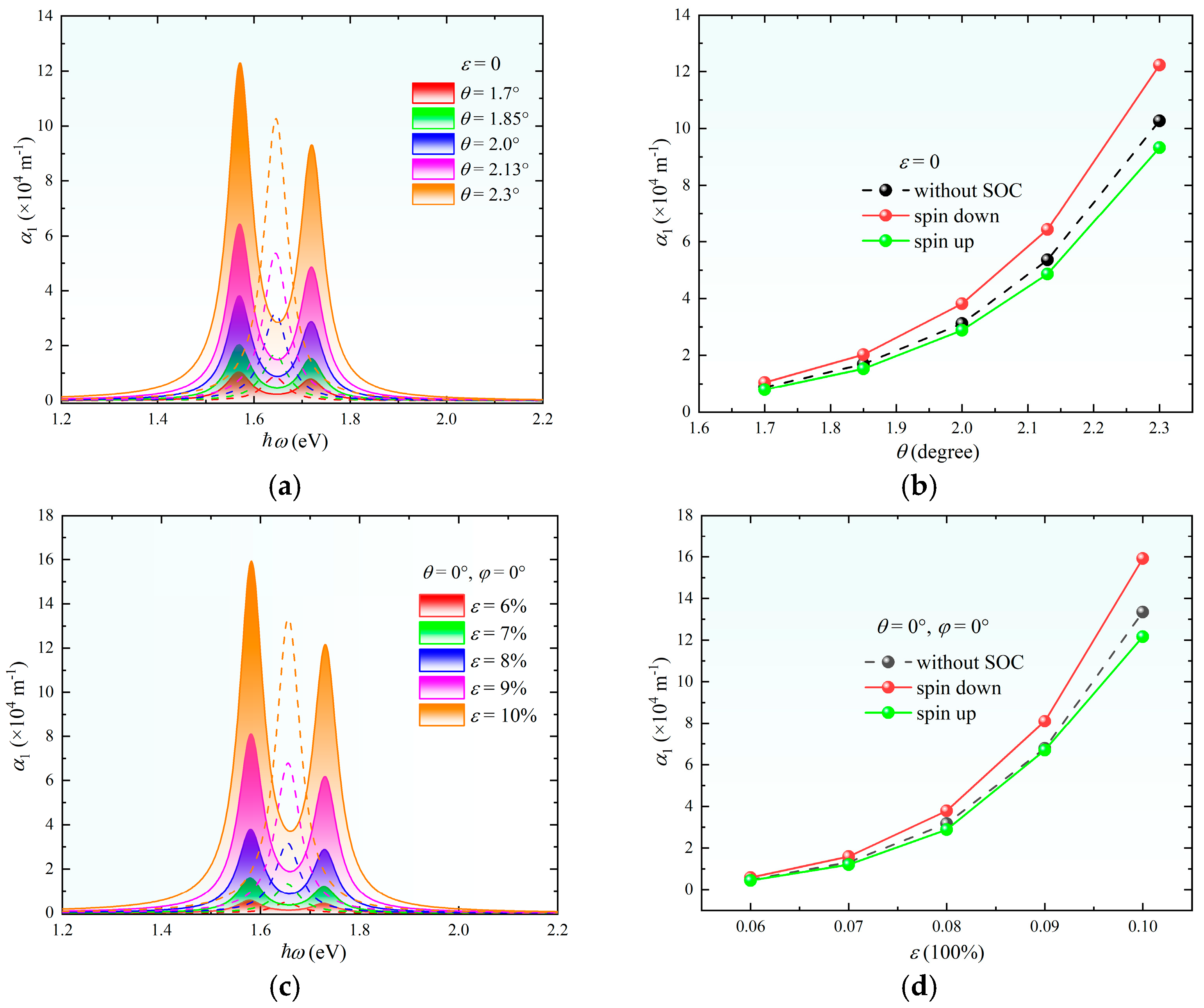
3.2. Single-Photon Absorption Coefficient
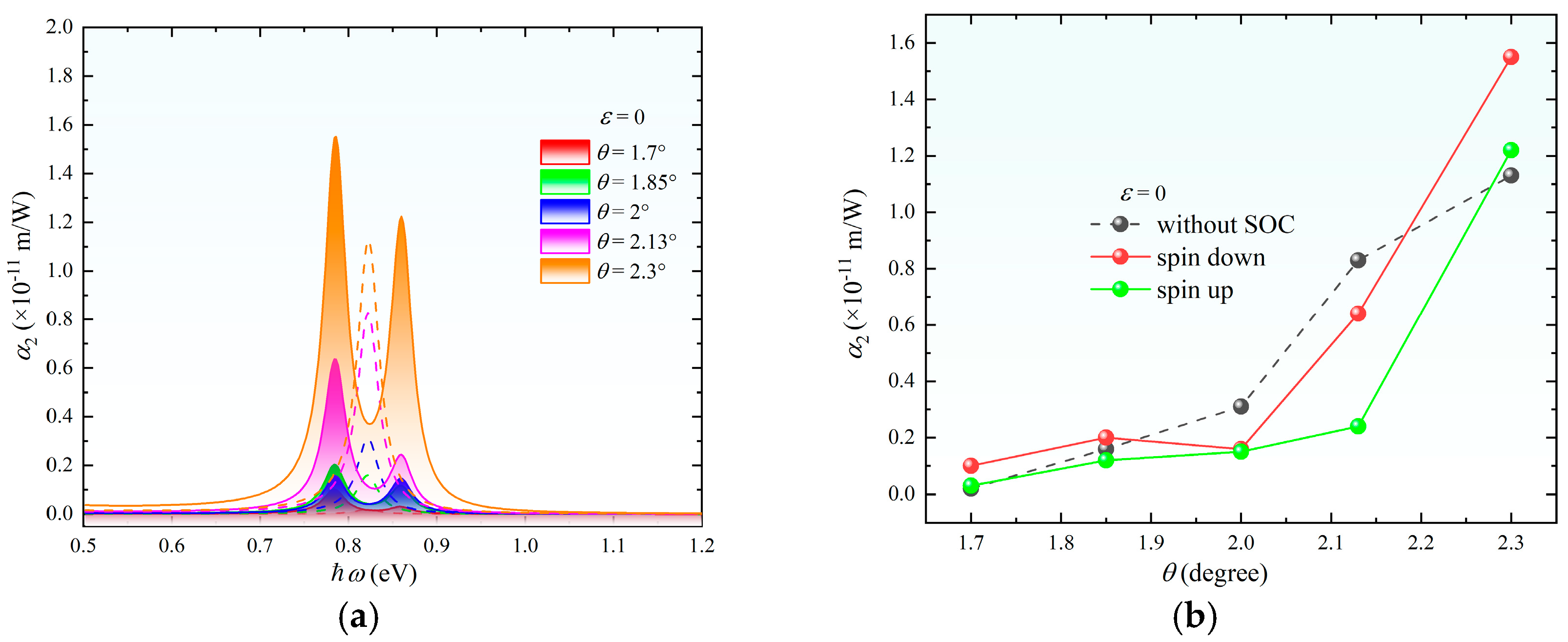
3.3. Two-Photon Absorption Coefficient
4. Conclusions
Author Contributions
Funding
Data Availability Statement
Conflicts of Interest
Abbreviations
| 2D | two-dimensional |
| TMDCs | transition metal dichalcogenides |
| SOC | spin-orbit coupling |
| PL | photoluminescence |
| OPA | one-photon absorption |
| TPA | two-photon absorption |
| MPA | multi-photon absorption |
| CBM | conduction band minimum |
| VBM | valence band maximum |
| ML-MoS2 | monolayer MoS2 |
| BL-MoS2 | bilayer MoS2 |
References
- Tombros, N.; Jozsa, C.; Popinciuc, M.; Jonkman, H.T.; Wees, B.J.V. Electronic spin transport and spin precession in single graphene layers at room temperature. Nature 2007, 448, 571–574. [Google Scholar] [CrossRef] [PubMed]
- Neto, A.H.C.; Guinea, F.; Peres, N.M.R.; Novoselov, K.S.; Geim, A.K. The electronic properties of graphene. Rev. Mod. Phys. 2009, 81, 109–162. [Google Scholar] [CrossRef]
- Rutter, G.M.; Crain, J.N.; Guisinger, N.P.; Li, T.; First, P.N.; Stroscio, J.A. Scattering and interference in epitaxial graphene. Science 2007, 317, 219–222. [Google Scholar] [CrossRef] [PubMed]
- Kim, K.; Choi, J.Y.; Kim, T.; Cho, S.H.; Chung, H.J. A role for graphene in silicon-based semiconductor devices. Nature 2011, 479, 338–344. [Google Scholar] [CrossRef] [PubMed]
- Novoselov, K.S.; Geim, A.K.; Morozov, S.V.; Jiang, D.; Zhang, Y.; Dubonos, S.V.; Grigorieva, I.V.; Firsov, A.A. Electric field effect in atomically thin carbon films. Science 2004, 306, 666–669. [Google Scholar] [CrossRef] [PubMed]
- Liu, H.; Neal, A.T.; Zhu, Z.; Luo, Z.; Xu, X.F.; Tománek, D.; Ye, P.D. Phosphorene: An unexplored 2D semiconductor with a high hole mobility. ACS Nano 2014, 8, 4033–4041. [Google Scholar] [CrossRef] [PubMed]
- Wang, Q.H.; Zadeh, K.K.; Kis, A.; Coleman, J.N.; Strano, M.S. Electronics and optoelectronics of two-dimensional transition metal dichalcogenides. Nat. Nanotechnol. 2012, 7, 699–712. [Google Scholar] [CrossRef] [PubMed]
- Chhowalla, M.; Shin, H.S.; Eda, G.; Li, L.J.; Loh, K.P.; Zhang, H. The chemistry of two-dimensional layered transition metal dichalcogenide nanosheets. Nat. Chem. 2013, 5, 263–275. [Google Scholar] [CrossRef] [PubMed]
- Sone, J.; Yamagami, T.; Aoki, Y.; Nakatsuji, K.; Hirayama, H. Epitaxial growth of silicene on ultra-thin Ag (111) films. New J. Phys. 2012, 16, 95004. [Google Scholar] [CrossRef]
- Dávila, M.E.; Xian, L.; Cahangirov, S.; Rubio, A.; Lay, G.L. Germanene: A novel two-dimensional germanium allotrope akin to graphene and silicene. New J. Phys. 2014, 16, 3579–3587. [Google Scholar] [CrossRef]
- Aivazian, G.; Gong, Z.; Jones, A.M.; Chu, R.L.; Yan, J.; Mandrus, D.G.; Zhang, C.; Cobden, D.; Yao, W.; Xu, X. Magnetic control of valley pseudospin in monolayer WSe2. Nat. Phys. 2015, 11, 148–152. [Google Scholar] [CrossRef]
- Srivastava, A.; Sidler, M.; Allain, A.V.; Lembke, D.S.; Kis, A.; Imamoğlu, A. Valley Zeeman effect in elementary optical excitations of monolayer WSe2. Nat. Phys. 2015, 11, 141–147. [Google Scholar] [CrossRef]
- Radisavljevic, B.; Radenovic, A.; Brivio, J.; Giacometti, V.; Kis, A. Single-layer MoS2 transistors. Nat. Nanotechnol. 2011, 6, 147–150. [Google Scholar] [CrossRef] [PubMed]
- Lee, H.S.; Min, S.W.; Chang, Y.G.; Park, M.K.; Nam, T.; Kim, H.; Kim, J.H.; Ryu, S.; Im, S. MoS2 nanosheet phototransistors with thickness-modulated optical energy gap. Nano Lett. 2012, 12, 3695–3700. [Google Scholar] [CrossRef] [PubMed]
- Park, Y.J.; Sharma, B.K.; Shinde, S.M.; Kim, M.S.; Jang, B.; Kim, J.H.; Ahn, J.H. All MoS2-based large area, skin-attachable active-matrix tactile sensor. ACS Nano 2019, 13, 3023–3030. [Google Scholar] [CrossRef] [PubMed]
- Ge, Y.C.; Chu, H.; Chen, J.Y.; Zhuang, P.Y.; Feng, Q.Y.; Smith, W.R.; Dong, P.; Ye, M.X.; Shen, J.F. Ultrathin MoS2 nanosheets decorated hollow CoP heterostructures for enhanced hydrogen evolution reaction. ACS Sustain. Chem. Eng. 2019, 7, 10105–10111. [Google Scholar] [CrossRef]
- Seh, Z.W.; Yu, J.H.; Li, W.Y.; Hsu, P.C.; Wang, H.T.; Sun, Y.M.; Yao, H.B.; Zhang, Q.F.; Cui, Y. Two-dimensional layered transition metal disulphides for effective encapsulation of high-capacity lithium sulphide cathodes. Nat. Commun. 2014, 5, 5017. [Google Scholar] [CrossRef] [PubMed]
- Naik, M.H.; Jain, M. Ultraflatbands and Shear Solitons in Moiré Patterns of Twisted Bilayer Transition Metal Dichalcogenides. Phys. Rev. Lett. 2018, 121, 266401.1–266401.6. [Google Scholar] [CrossRef] [PubMed]
- Zhang, Z.; Wang, Y.; Watanabe, K.; Taniguchi, T.; Ueno, K.; Tutuc, E.; LeRoy, B.J. Flat bands in twisted bilayer transition metal dichalcogenides. Nat. Phys. 2020, 16, 1093–1096. [Google Scholar] [CrossRef]
- Zhan, Z.; Zhang, Y.; Lv, P.; Zhong, H.; Yu, G.; Guinea, F.; Silva-Guillén, J.A.; Yuan, S. Tunability of multiple ultraflat bands and effect of spin-orbit coupling in twisted bilayer transition metal dichalcogenides. Phys. Rev. B 2020, 102, 241106. [Google Scholar] [CrossRef]
- Oshima, S.; Toyoda, M.; Saito, S. Geometrical and electronic properties of unstrained and strained transition metal dichalcogenide nanotubes. Phys. Rev. Mater. 2020, 4, 026004. [Google Scholar] [CrossRef]
- Naumis, G.G.; Herrera, S.A.; Poudel, S.P.; Nakamura, H.; Barraza-Lopez, S. Mechanical, electronic, optical, piezoelectric and ferroic properties of strained graphene and other strained monolayers and multilayers: An update. Rep. Prog. Phys. 2023, 87, 016502. [Google Scholar] [CrossRef] [PubMed]
- He, K.; Poole, C.; Mak, K.F.; Shan, J. Experimental demonstration of continuous electronic structure tuning via strain in atomically thin MoS2. Nano Lett. 2013, 13, 2931–2936. [Google Scholar] [CrossRef] [PubMed]
- Lin, K.Q.; Faria Junior, P.E.; Bauer, J.M.; Peng, B.; Monserrat, B.; Gmitra, M.; Fabian, J.; Bange, S.; Lupton, J.M. Twist-angle engineering of excitonic quantum interference and optical nonlinearities in stacked 2D semiconductors. Nat. Commun. 2021, 12, 1553. [Google Scholar] [CrossRef] [PubMed]
- Xiao, D.; Liu, G.-B.; Feng, W.; Xu, D.; Yao, W. Coupled spin and valley physics in monolayers of MoS2 and other group-VI dichalcogenides. Phys. Rev. Lett. 2012, 108, 196802. [Google Scholar] [CrossRef] [PubMed]
- Xiao, D.; Yao, W.; Niu, Q. Valley-contrasting physics in graphene: Magnetic moment and topological transport. Phys. Rev. Lett. 2007, 99, 236809. [Google Scholar] [CrossRef] [PubMed]
- Yao, W.; Xiao, D.; Niu, Q. Valley-dependent optoelectronics from inversion symmetry breaking. Phys. Rev. B 2008, 77, 235406. [Google Scholar] [CrossRef]
- Bi, Z.; Yuan, N.F.Q.; Fu, L. Designing flat bands by strain. Phys. Rev. B 2019, 100, 035448. [Google Scholar] [CrossRef]
- Yu, L.; Fu, Z.; Yang, P.; Feng, X. Strain-enhanced two-photon absorption in twisted bilayer graphene. Sci. Rep. 2025, 15, 15565. [Google Scholar] [CrossRef] [PubMed]
- Yue, Q.; Kang, J.; Shao, Z.; Zhang, X.; Chang, S.; Wang, G.; Qin, S.; Li, J. Mechanical and electronic properties of monolayer MoS2 under elastic strain. Phys. Lett. A 2012, 376, 1166–1170. [Google Scholar] [CrossRef]
- Fang, S.; Carr, S.; Cazalilla, M.A.; Kaxiras, E. Electronic structure theory of strained two-dimensional materials with hexagonal symmetry. Phys. Rev. B 2018, 98, 075106.1–075106.13. [Google Scholar] [CrossRef]
- Javvaji, S.; Sun, J.H.; Jung, J. Topological flat bands without magic angles in massive twisted bilayer graphenes. Phys. Rev. B 2020, 101, 125411. [Google Scholar] [CrossRef]
- Nathan, V.; Guenther, A.H.; Mitra, S.S. Review of multiphoton absorption in crystalline solids. J. Opt. Soc. Am. B 1985, 2, 294–316. [Google Scholar] [CrossRef]
- Ramasubramaniam, A.; Naveh, D.; Towe, E. Tunable band gaps in bilayer transition-metal dichalcogenides. Phys. Rev. B 2011, 84, 3239–3247. [Google Scholar] [CrossRef]
- Liu, Q.; Li, L.; Li, Y.; Gao, Z.; Chen, Z.; Lu, J. Tuning electronic structure of bilayer MoS2 by vertical electric field: A first-principles investigation. J. Phys. Chem. C 2012, 116, 21556–21562. [Google Scholar] [CrossRef]
- Zhang, Z.; Li, J.; Yang, G.; Ouyang, G. Interface engineering of band evolution and transport properties of bilayer WSe2 under different electric fields. J. Phys. Chem. C 2019, 123, 19812–19819. [Google Scholar] [CrossRef]
- Liu, G.B.; Shan, W.Y.; Yao, Y.; Yao, W.; Xiao, D. Three-band tight-binding model for monolayers of group-VIB transition metal dichalcogenides. Phys. Rev. B 2013, 88, 085433. [Google Scholar] [CrossRef]
- Li, Y.X.; Dong, N.N.; Zhang, S.F.; Zhang, X.Y.; Feng, Y.Y.; Wang, K.P.; Zhang, L.; Wang, J. Giant two-photon absorption in monolayer MoS2. Laser Photonics Rev. 2015, 9, 427. [Google Scholar] [CrossRef]
- Zhou, F.; Kua, J.H.; Lu, S.; Ji, W. Two-photon absorption arises from two-dimensional excitons. Opt. Express 2018, 26, 16093. [Google Scholar] [CrossRef] [PubMed]
- Gong, R.; Zhou, C.; Feng, X. Magnetic field dependent two-photon absorption properties in monolayer MoS2. Phys. Rev. B 2022, 105, 195301. [Google Scholar] [CrossRef]
- Dong, N.N.; Li, Y.X.; Zhang, S.F.; McEvoy, N.; Gatensby, R.; Duesberg, G.S.; Wang, J. Saturation of two-photon absorption in layered transition metal dichalcogenides: Experiment and theory. ACS Photonics 2018, 5, 1558. [Google Scholar] [CrossRef]
- Zhang, S.F.; Dong, N.N.; McEvoy, N.; O’Brien, M.; Winters, S.; Berner, N.C.; Yim, C.Y.; Li, Y.X.; Zhang, X.Y.; Chen, Z.H.; et al. Direct observation of degenerate two-photon absorption and saturation in WS2 and MoS2 monolayer and few-layer films. ACS Nano 2015, 9, 7142. [Google Scholar] [CrossRef] [PubMed]


| Thickness | Electric Field (V/Å) | Twist Angle (Degree) | Strain Magnitude (%) | Wavelength (nm) | β (Experiment) (m/W) | β (Other Theory) (m/W) | β (This Theory) (m/W) |
|---|---|---|---|---|---|---|---|
| ML-MoS2 | 0 | 0 | 0 | 1030 | (7.62 ± 0.15) × 10−8 [38] | ||
| ML-MoS2 | 0 | 0 | 0 | 800 | 8 × 10⁻⁹ [39] | ||
| ML-MoS2 | 0 | 0 | 0 | 780 | 7.47 × 10⁻¹¹ [40] | ||
| ML-MoS2 | 0 | 0 | 0 | 1030 | 4.2 × 10⁻¹¹ [40] | ||
| 50.0 ± 0.75 (nm) | 0 | 0 | 0 | 1030 | (4.99 ± 0.02) × 10−9 [41] | ||
| 25–27 layers | 0 | 0 | 0 | 800 | (6.6 ± 0.4) × 10−10 [42] | ||
| 25–27 layers | 0 | 0 | 0 | 1030 | (1.14 ± 4.3) × 10−10 [42] | ||
| BL-MoS2 | 0 | 1.7 | 0 | 1506 ± 60 | 0.1 × 10⁻¹¹ | ||
| BL-MoS2 | 0 | 2.3 | 0 | 1506 ± 60 | 1.55 × 10⁻¹¹ | ||
| BL-MoS2 | 0 | 0 | 6 | 1506 ± 60 | 0.1 × 10⁻¹¹ | ||
| BL-MoS2 | 0 | 0 | 10 | 1506 ± 60 | 2.0 × 10⁻¹¹ | ||
| BL-MoS2 | 0 | 1.85 | 2 | 1469 ± 60 | 0.1 × 10⁻⁹ | ||
| BL-MoS2 | 0 | 1.85 | 10 | 1469 ± 60 | 0.85 × 10⁻⁹ | ||
| BL-MoS2 | 0.01 | 2.13 | 0 | 1627 | 3.62 × 10⁻¹² | ||
| BL-MoS2 | 0.05 | 2.13 | 0 | 1902 | 0.46 × 10⁻¹² | ||
| BL-MoS2 | 0.01 | 3.15 | 0 | 1623 | 1.62 × 10⁻¹¹ | ||
| BL-MoS2 | 0.05 | 3.15 | 0 | 1914 | 2.27 × 10⁻¹¹ |
Disclaimer/Publisher’s Note: The statements, opinions and data contained in all publications are solely those of the individual author(s) and contributor(s) and not of MDPI and/or the editor(s). MDPI and/or the editor(s) disclaim responsibility for any injury to people or property resulting from any ideas, methods, instructions or products referred to in the content. |
© 2025 by the authors. Licensee MDPI, Basel, Switzerland. This article is an open access article distributed under the terms and conditions of the Creative Commons Attribution (CC BY) license (https://creativecommons.org/licenses/by/4.0/).
Share and Cite
Yu, L.; Chen, Y.; Zhang, W.; Yang, P.; Feng, X. Spin-Orbit-Coupling-Governed Optical Absorption in Bilayer MoS2 via Strain, Twist, and Electric Field Engineering. Nanomaterials 2025, 15, 1100. https://doi.org/10.3390/nano15141100
Yu L, Chen Y, Zhang W, Yang P, Feng X. Spin-Orbit-Coupling-Governed Optical Absorption in Bilayer MoS2 via Strain, Twist, and Electric Field Engineering. Nanomaterials. 2025; 15(14):1100. https://doi.org/10.3390/nano15141100
Chicago/Turabian StyleYu, Lianmeng, Yingliang Chen, Weibin Zhang, Peizhi Yang, and Xiaobo Feng. 2025. "Spin-Orbit-Coupling-Governed Optical Absorption in Bilayer MoS2 via Strain, Twist, and Electric Field Engineering" Nanomaterials 15, no. 14: 1100. https://doi.org/10.3390/nano15141100
APA StyleYu, L., Chen, Y., Zhang, W., Yang, P., & Feng, X. (2025). Spin-Orbit-Coupling-Governed Optical Absorption in Bilayer MoS2 via Strain, Twist, and Electric Field Engineering. Nanomaterials, 15(14), 1100. https://doi.org/10.3390/nano15141100