Article

Relation Between Thickness and TFTs Properties of HfO2 Dielectric Layer Synthesized by Plasma-Enhanced Atomic Layer Deposition

1
Xiamen Key Laboratory of Development and Application for Advanced Semiconductor Coating Technology, School of Opto-Electronic and Communication Engineering, Xiamen University of Technology, Xiamen 361024, China
2
Department of Materials Science and Engineering, Da-Yeh University, Dacun, Changhua 51591, Taiwan
*
Author to whom correspondence should be addressed.
Nanomaterials 2025, 15(10), 719; https://doi.org/10.3390/nano15100719
Submission received: 15 April 2025 / Revised: 2 May 2025 / Accepted: 7 May 2025 / Published: 10 May 2025

Abstract

:
The advancement of portable high-definition organic light-emitting diode (OLED) displays necessitates thin film transistors (TFTs) with low power consumption and high pixel density. Amorphous indium gallium zinc oxide (a-IGZO) TFTs are promising candidates to meet these requirements. However, conventional silicon dioxide gate insulators provide limited channel modulation due to their low dielectric constant, while alternative high-k dielectrics often suffer from high leakage currents and poor surface quality. Plasma-enhanced atomic layer deposition (PEALD) enables the atomic-level control of film thickness, resulting in high-quality films with superior conformality and uniformity. In this work, a systematic investigation was conducted on the properties of HfO2 films and the electrical characteristics of a-IGZO TFTs with different HfO2 thicknesses. A Vth of −0.9 V, μsat of 6.76 cm2/Vs, SS of 0.084 V/decade, and Ion/Ioff of 1.35 × 10⁹ are obtained for IGZO TFTs with 40 nm HfO2. It is believed that the IGZO TFTs based on a HfO2 gate insulating layer and prepared by PEALD can improve electrical performance.

1. Introduction

Active-matrix organic light-emitting diodes (AMOLEDs) are a leading display technology, consisting of organic light-emitting pixels, thin film transistors (TFTs), and storage capacitance [1,2,3,4,5]. Among these components, the performance of TFTs is particularly critical for AMOLED functionality, driving extensive research into optimizing their channel layers. Amorphous indium gallium zinc oxide (a-IGZO) TFTs have become highly attractive as promising candidates for switching and driving devices in active-matrix electronics due to their high carrier mobility, large switching current ratio, excellent uniformity, and optical transparency in the visible spectrum [6,7,8]. While significant attention has been given to improving channel layer properties, the role of gate insulators is equally crucial. The characteristics of the gate insulator directly influence the threshold voltage (Vth), subthreshold swing (SS), and overall electrical stability of TFTs.
Conventional gate dielectrics such as silicon dioxide (SiO2) and silicon nitride (Si3N4) are limited by their relatively low dielectric constants (k), which lead to weak channel modulation and require high driving voltages [9,10,11]. These shortcomings result in increased power consumption and reduced device lifespan, particularly in next-generation flexible and high-resolution displays. To address these challenges, two major strategies have been proposed: (1) reducing the thickness of gate insulators and (2) employing high-k dielectric materials. While thinner dielectric films can lower operating voltages, they often suffer from degraded quality and increased leakage currents. Adopting high-k gate dielectric materials can minimize the physical thickness of a gate insulator to achieve a high current with a low operating voltage, because of the large gate capacitance. Hafnium oxide (HfO2) is a particularly attractive high-k dielectric due to its thermodynamic stability, high dielectric constant, and excellent electrical performance under high drive currents. However, challenges such as high leakage current, poor surface morphology, and the formation of trap states at the dielectric/channel interface still hinder its practical application in TFTs.
Therefore, optimizing both the thickness and the interfacial quality of HfO2 films is critical for enhancing TFT device performance. Various deposition methods have been explored for fabricating high-k dielectric layers. Although methods such as molecular beam epitaxy (MBE) and chemical vapor deposition (CVD) offer high deposition rates, their high processing temperatures limit their applicability to the flexible substrates and low-temperature processes required for display integration [12,13,14]. Atomic layer deposition (ALD) enables atomic-scale thickness control and excellent step coverage, making it suitable for ultrathin, conformal dielectric films. Plasma-enhanced atomic layer deposition (PEALD), a variant of ALD, further improves film quality by providing higher film density, smoother surfaces, and better interfacial characteristics due to enhanced plasma reactivity. These advantages contribute to reduced interface trap density, improved SS, enhanced carrier mobility, and lower leakage currents in oxide TFTs—making PEALD a highly promising technique for advanced electronics.
In this work, the effect of HfO2 film thickness was systematically investigated, with deposition by PEALD, including the optical and electrical properties of the dielectric layer and the performance of a-IGZO TFTs. HfO2 films with thicknesses of 20, 40, 60, and 80 nm were deposited, and their influence on capacitance, leakage current, and device switching behavior was comprehensively evaluated. This work provides new insights into thickness optimization strategies for high-k dielectrics in TFT applications and highlights the potential of PEALD-grown HfO2 films for next-generation electronics.

2. Materials and Methods

Heavily doped p-type (100) silicon wafers (p++-Si, ρ < 0.001 Ω·cm) (Shandong Zhuojing Electronic Technology Co., Ltd., Jinan, China) were used as both the substrate and gate electrode. The wafers were diced into 2.5 × 2.5 cm2 pieces and underwent a three-step cleaning process to ensure surface preparation. First, the substrates were soaked in deionized water for 10 s, followed by immersion in a 2% diluted hydrofluoric acid solution (Sinopharm Chemical Reagent Co., Ltd., Shanghai, China) for 1 min, and finally rinsed again in deionized water for 10 s. After cleaning, the wafers were immediately dried with a nitrogen blower and transferred into the reaction chamber of PEALD. HfO2 thin films with thicknesses of 20, 40, 60, and 80 nm were deposited using tetrakis(ethylmethylamino)hafnium (TEMAH, purity: 99.9999%, AimouYuan, Nanjing, China) and O2/Ar plasma (produced in a microwave cavity by an inductive coupling of radio frequency (RF) power (Litmas RPS, Advanced Energy, Denver, CO, USA)) in a PEALD system (Picosun R-200, Espoo, Finland) at temperatures ranging from 100 to 450 °C, with a plasma power of 2500 W; each ALD cycle consisted of a 1.6 s TEMAH pulse, 10 s N2 purge, 10 s plasma exposure, and 12 s N2 purge [15]. A 30 nm amorphous indium gallium zinc oxide (a-IGZO) channel layer, with a 35% In2O3 cycle ratio, was also deposited using the same PEALD system following previously reported procedures [16]. The IGZO thin films were fabricated by stacking PEALD-grown ZnO, Ga2O3, and In2O3 sub-layers using DEZ, TMGa, and InCp (Nanjing Aimuyuan Scientific Equipment Co., Ltd., Nanjing, China) as respective precursors, with an O2 plasma power of 2500 W and a deposition temperature of 250 °C. The active layer was patterned into a square shape with dimensions of 1000 μm. The aluminum source and drain electrode with a thickness of 150 nm were prepared by thermal vacuum deposition, and a shadow mask (Shenzhen Kebaoyuan Technology Co., Ltd., Shenzhen, China) was employed to create a patterned channel with dimensions of 80 μm in length and 1000 μm in width.
The capacitance characteristics of the HfO2 film and electronic characteristics of the a-IGZO TFT based on HfO2 film were measured by a semiconductor parameter analyzer (200-SCS, Keithley Instruments Inc., Beaverton, OR, USA) at room temperature under an ambient atmosphere. The thickness of the HfO2 film was determined using a step profiler (D-500, KLA-Tencor Corp., Milpitas, CA, USA). The crystalline structure of HfO2 films was analyzed via grazing incident X-ray diffraction (GIXRD, TTRAX III, Rigaku Corp., Ibaraki, Japan). The root-mean-square (RMS) surface roughness was assessed using an atomic force microscope (AFM, XE7, Park Systems Corp., Suwon, Republic of Korea). The surface morphologies of HfO2 films were examined using field emission scanning electron microscopy (FESEM, Sigma 500, Carl Zeiss AG, Oberkochen, Germany). Additionally, the cross-section images of the a-IGZO TFT device were scrutinized using field emission transmission electron microscopy (FE-TEM, JEM-2100F, JEOL Ltd., Tokyo, Japan).

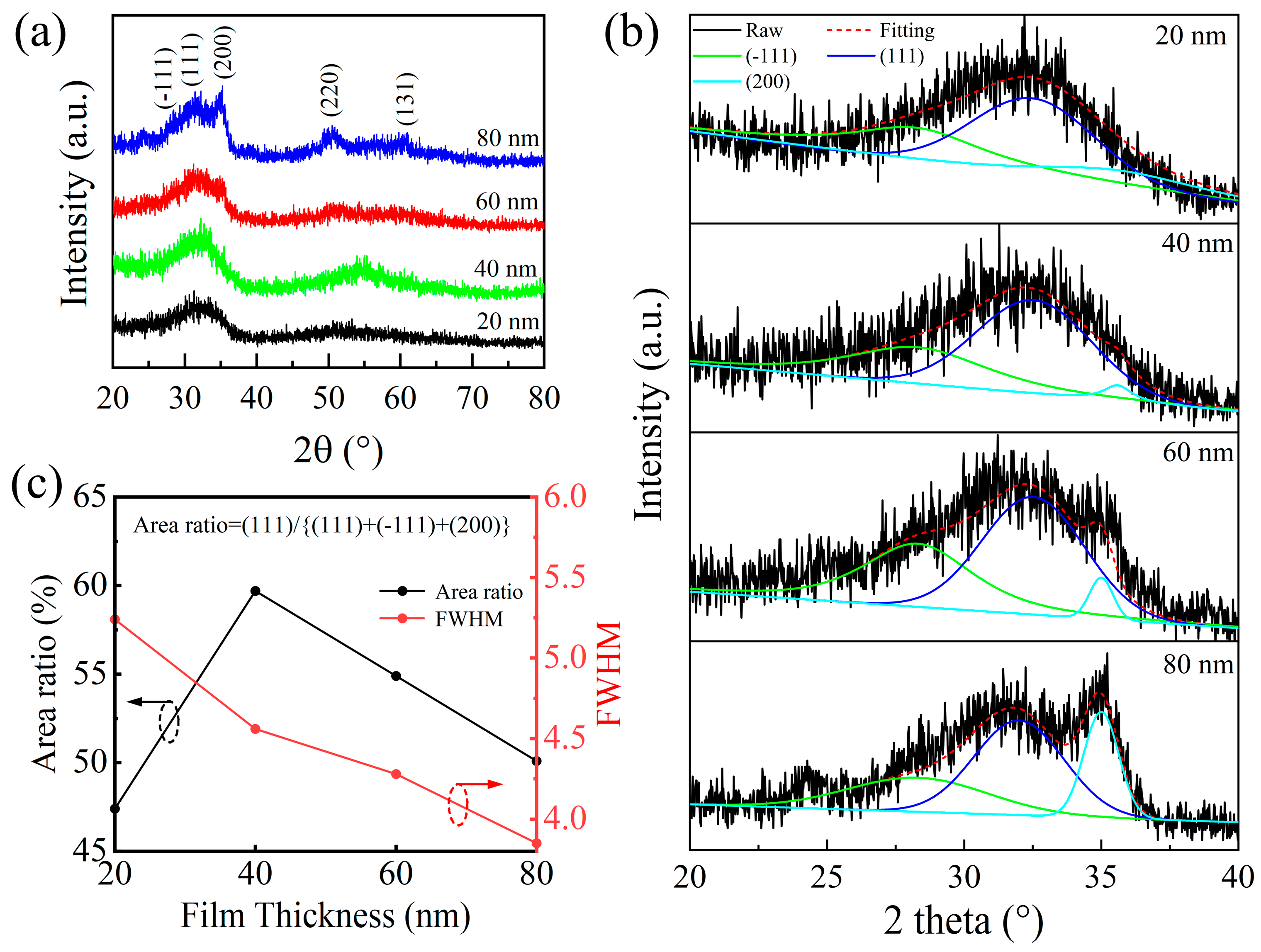
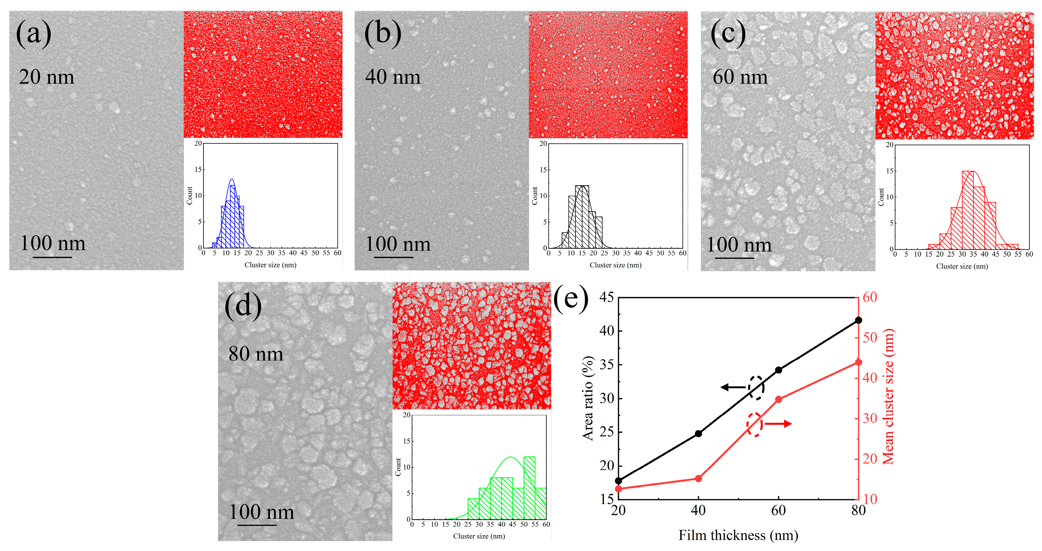
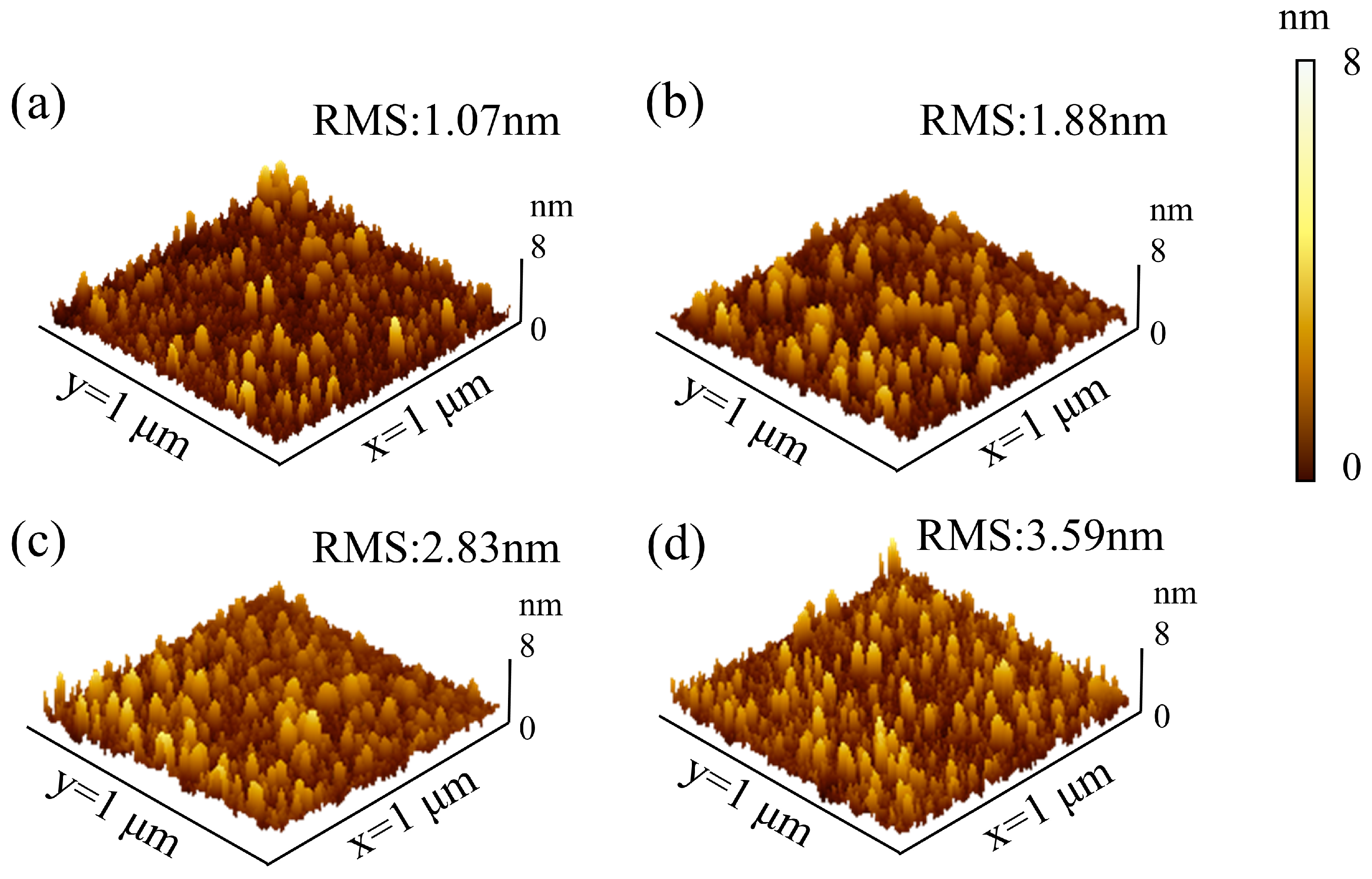
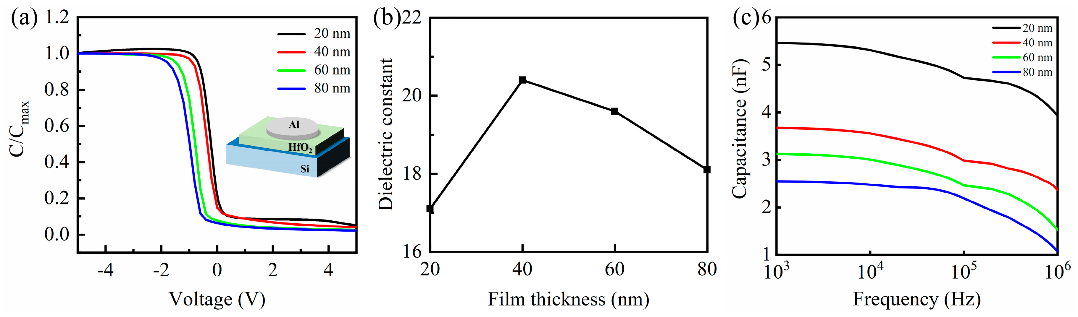
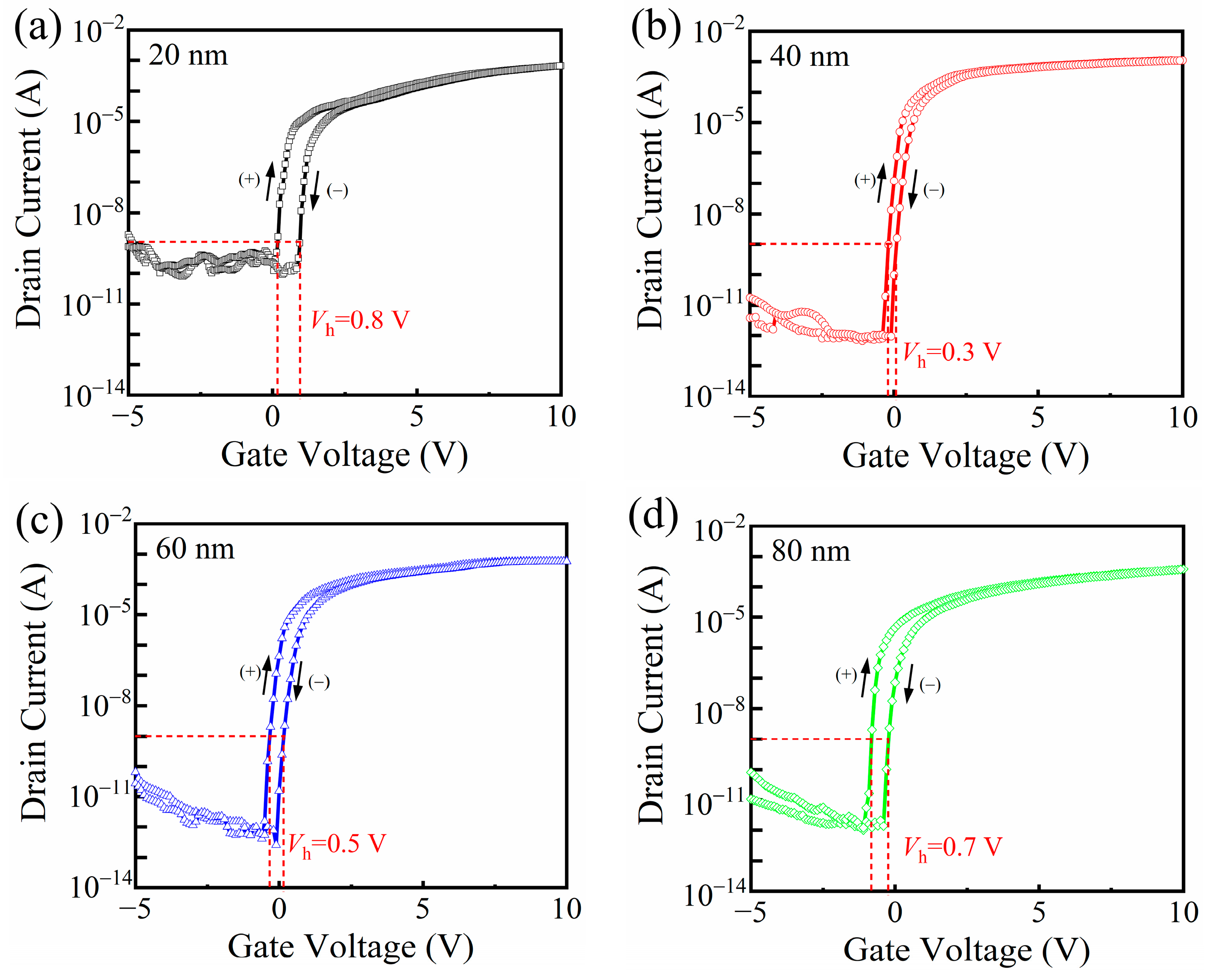
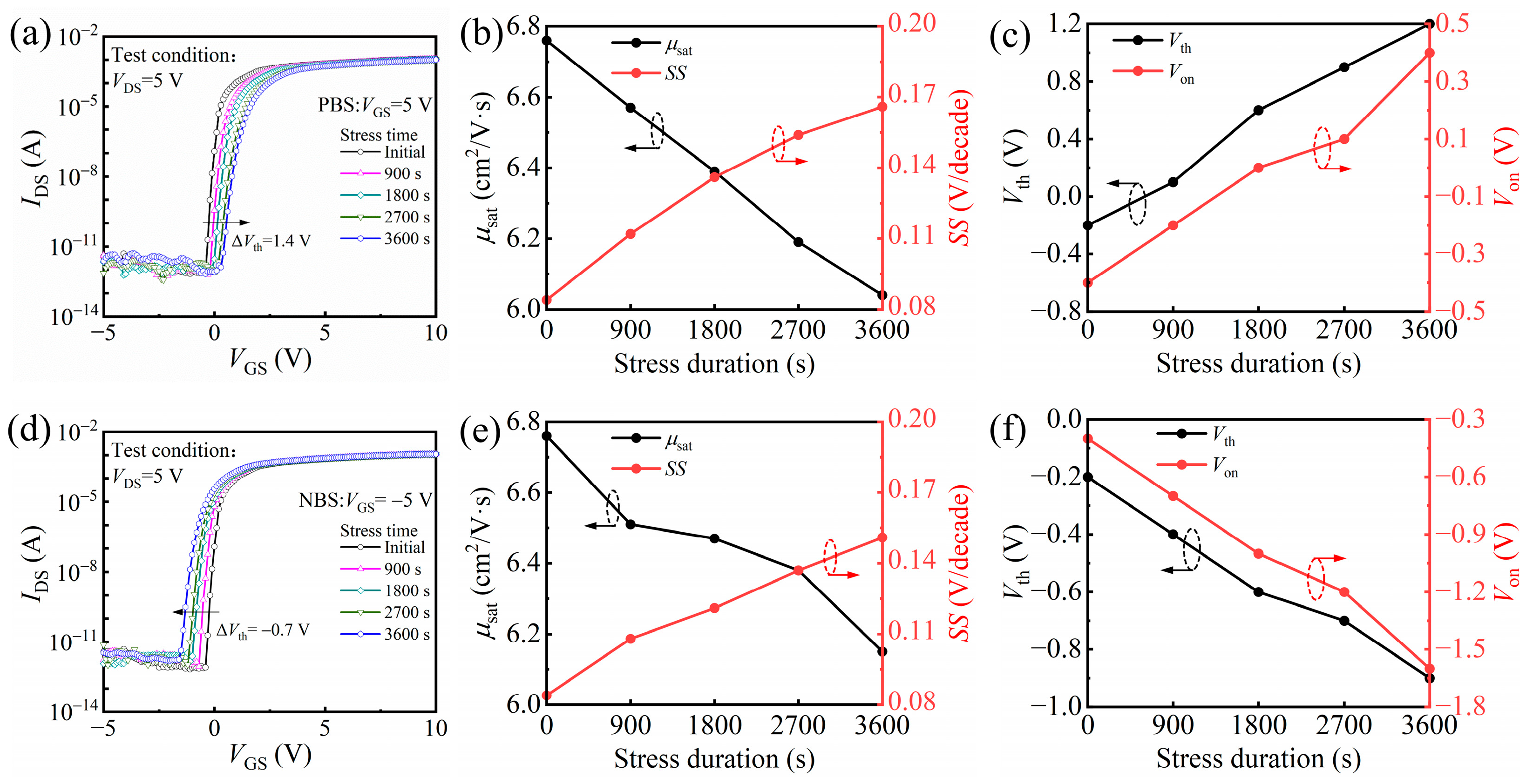
3. Results and Discussion

The thickness of the gate insulator and the quality of its interface are critical factors influencing TFT performance. To assess the structural properties of the HfO2 films, GIXRD measurements were performed on samples with varying thicknesses, as shown in Figure 1a. Diffraction peaks were observed at 2θ = 28.31°, 31.44°, and 35.60°, corresponding to the (−111), (111), and (200) planes, respectively, as indexed for HfO2 in the standard JCPDS file (data No. 06-0318). As the film thickness increases from 20 to 80 nm, the overall crystallinity improves, evidenced by the increasing intensity of the diffraction peaks. The detailed GIXRD spectra of the HfO2 films with varying thickness were deconvoluted, as shown in Figure 1b. The intensities of all diffraction peaks increase with film thickness, with particular emphasis on the (111) peak, as it significantly influences the dielectric constant of the films [17,18,19]. The (111) peak area ratio relative to the total diffraction intensity, plotted in Figure 1c, reaches a maximum at 40 nm and then declines, suggesting an optimal crystalline orientation at this thickness. Moreover, the full width at half-maximum (FWHM) of the (111) peak decreases with increasing thickness, indicating reduced lattice disorder and improved grain quality. Specifically, when the film thickness is small, surface energy dominates, and the film tends to form an amorphous or low-crystallinity structure [20,21,22,23,24]. As the film thickens, grain growth and packing density are enhanced, resulting in improved crystallinity. Notably, the 40 nm HfO2 film demonstrates the most favorable structural characteristics, which are expected to translate into superior dielectric performance.
FESEM was employed to analyze the surface morphology of HfO2 films with varying thicknesses, as shown in Figure 2. The 20 nm film (Figure 2a) displays small, uniformly distributed grains/clusters, with size statistics shown in the inset. As the film thickness increases (Figure 2b–d), both the grain/cluster size and coverage area expand. Quantitative analysis using ImageJ software (version 1.54f, developed by the National Institutes of Health, Bethesda, MD, USA) shows that the grain/cluster area ratio increases from 17.78% at 20 nm to 41.61% at 80 nm, while the mean cluster size grows from 12.64 nm to 43.99 nm (Figure 2e). Interestingly, the 40 nm film shows only a modest increase in grain size compared to the 20 nm film, suggesting a transitional regime in morphology evolution.
Complementary AFM measurements (Figure 3a–d) further confirm the surface morphology trends. The root-mean-square (RMS) roughness increases progressively with thickness, from 1.07 nm at 20 nm to 3.59 nm at 80 nm, consistent with the growth of grains/clusters observed in SEM. Notably, the 20 nm and 40 nm films exhibit relatively smooth and continuous surfaces with low roughness and minimal island formation, while the 60 nm and 80 nm films develop more pronounced surface textures and grain boundaries. These findings indicate that the surface morphology of HfO2 evolves significantly with thickness, with smoother, denser films at thinner regions and rougher, more granular structures at greater thicknesses.
The capacitance and dielectric constant (k) are key parameters that directly affect the electrical performance of the gate insulator in TFTs, and both are influenced by film thickness and interfacial quality. Figure 4a presents the C–V curves of n-Si/HfO2/Al MOS capacitors measured at 1 MHz for HfO2 films with varying thicknesses. The capacitance in the accumulation region was extracted from the voltage range of −5 V to +10 V, corresponding to the maximum capacitance (Cmax). The measured Cmax values were 3.88 × 10⁻⁹ F, 2.36 × 10⁻⁹ F, 1.53 × 10⁻⁹ F, and 1.06 × 10⁻⁹ F for HfO2 thicknesses of 20, 40, 60, and 80 nm, respectively. Figure 4b shows the relationship between film thickness and the dielectric constant k, which is calculated using the following equation [25,26]:
k = C m a x A d ε 0
where d stands for the thickness of the HfO2 film, A is the area of the capacitor (5.28 × 10⁻⁷ m2), and ε0 is the dielectric constant of the vacuum. Capacitance per unit area (Cox) was calculated as 73.5, 44.7, 29.0, and 20.1 nF/cm2 for 20, 40, 60, and 80 nm, respectively, exhibiting a decreasing trend with increasing thickness. The calculated k values initially increased from 17.1 (20 nm) to a peak of 20.4 (40 nm) and then declined to 18.1 (80 nm). This trend is attributed to the improved crystallinity and packing density at intermediate thicknesses, particularly the enhanced (111) orientation at 40 nm, which is known for its high polarizability [17,18,19]. Beyond 40 nm, although crystallinity continues to improve, the relative intensity of the (111) plane decreases (as shown in Figure 1c), leading to a reduction in the effective dielectric constant. To further evaluate the frequency-dependent behavior of the HfO2 films, capacitance–frequency (C–f) measurements were conducted for samples with thicknesses of 20, 40, 60, and 80 nm, as shown in Figure 4c. The capacitance (C) was extracted from the accumulation region in the frequency range of 1 kHz to 1 MHz. All samples exhibited relatively stable capacitance values across the measured frequencies, indicating good dielectric reliability and low interface trap density. The 20 nm film showed the highest capacitance, while the 40 nm film exhibited the smallest variation with frequency, suggesting the best overall dielectric and interface stability at this thickness. The fixed charge (Qf) is determined from the C–V characteristics, as reported in [27,28]:
Q f = ( φ m s V F B ) C o x q   A
φms (0.3 eV) represents the work function difference between the metal and the semiconductor, while VFB denotes the flat band voltage. Although Cox decreases with thickness, Qf increases due to a more negative shift in VFB (from −0.20 V at 20 nm to −0.97 V at 80 nm), indicating the accumulation of negative fixed charges and bulk defects in thicker films. The interface charge density (Dit) was calculated from the C–V characteristics using the following expression [29,30]:
D i t = 2 ω C o x 2 G m a x q A ( G m a x 2 + ω 2 ( C o x C m G m a x ) 2 )
The maximum conductance, Gmax, and the measured capacitance, Cm, at an angular frequency ω are considered in this expression. The 20 nm HfO2 film exhibits an amorphous structure, which is advantageous for the passivation of Si surfaces, thereby minimizing the Dit. Table 1 summarizes the extracted values of Dit and Qf for all film thicknesses, both of which increase with thickness and are strongly correlated with the degradation in TFT electrical parameters such as Vth, μsat, and SS.
To evaluate the electronic performance of TFTs with different HfO2 thicknesses, devices with the Si/HfO2/IGZO/Al structure were prepared, and their 3D schematic diagram is presented in Figure 5a. To verify the interface quality between the HfO2 gate insulator and the IGZO channel layer, cross-sectional FE-TEM was performed on the TFT with a 40 nm HfO2 layer, as shown in Figure 5b. The observed uniform interface is favorable for minimizing the subthreshold swing (SS) by suppressing interfacial trap states. The transfer characteristics, shown in Figure 5c, exhibit typical n-type behavior. Measurements were performed at a drain-source voltage (VDS) of 5 V, while the gate voltage (VGS) was swept from −5 V to 10 V. The on/off current ratio (Ion/Ioff) is negatively related to the thickness, and it decreased from 1.35 × 10⁹ to 3.32 × 10⁸ as the thickness increased from 20 nm to 80 nm. The Vth shifts negatively with increasing thickness, measuring −0.1 V, −0.2 V, −0.4, and −1.1 V for thicknesses of 20 to 80 nm, respectively, corresponding with the Qf. The SS was extracted using the standard method [31]:
S S = d V G S d ( l o g 10 I D S )
The saturation field-effect mobility (μsat) was calculated using the following equation:
I D S = W 2 L μ s a t C o x ( V G S V t h ) 2
where W and L are the channel width and length. This method follows the standard extraction approach reported in [32]. The device with 40 nm HfO2 film demonstrates an exceptionally low SS value of 0.084 V/decade; meanwhile, the μsat of the device is 6.76 cm2/Vs. These improvements are attributed to a reduction in interfacial trap density (Nt), which was calculated using the following equation [33,34,35]:
N t = S S l o g 1 0 e k B T q - 1 C o x q
where q is the electron charge, kB is Boltzmann’s constant, and T is the absolute temperature. The minimum Nt value of 1.14 × 1012 cm−2 was observed at 40 nm, indicating enhanced carrier transport at the HfO2/IGZO interface. Meanwhile, the leakage current of the device is also shown in Figure 5c, further demonstrating the compactness of the HfO2 film and overcoming the inherent defects in most high-k dielectrics. Figure 5d shows the output characteristics of the a-IGZO TFT with a 40 nm HfO2 gate dielectric. The device exhibits well-defined linear and saturation regions, and the smooth increase in drain current with gate bias confirms effective gate modulation and good ohmic contact. These results support the superior performance observed at the 40 nm dielectric thickness. The extracted electrical parameters for all devices are summarized in Table 1. The electrical parameters of the a-IGZO TFTs exhibit clear trends with respect to HfO2 thickness. The Vth progressively shifts in the negative direction as thickness increases. Both the μsat and on/off current ratio improve up to 40 nm, after which they begin to decline. Similarly, the SS reaches a minimum at 40 nm, confirming improved interfacial quality at this thickness. These results suggest that moderate dielectric thickness offers a favorable balance between interface quality and gate modulation efficiency, while excessively thick films introduce trap states and reduce gate controllability. In contrast, the 20 nm HfO2 film exhibits inferior performance due to its predominantly amorphous structure, which leads to a higher leakage current and a lower dielectric constant. These observations demonstrate that a moderate dielectric thickness offers an optimal trade-off between gate capacitance, interfacial quality, and electrical stability. Compared with the previous work on a transparent IGZO TFT prepared by PEALD and PEALD-deposited aluminum hafnium mixed oxide dielectrics for a-IGZO TFTs, the high-dielectric-constant insulation layer and high-quality surface morphology enable the device to achieve a higher Ion/Ioff and an ideal SS [36]. To evaluate the large-area uniformity of device performance, five 2.5 × 2.5 cm2 substrates were placed at representative positions within the 8-inch loading zone of the PEALD chamber: top-left, top-right, bottom-left, bottom-right, and center. On each substrate, a 5 × 5 array of a-IGZO TFTs (25 devices) was fabricated. One device was randomly selected from each array for electrical testing. As summarized in Table 1, the μsat and SS exhibited standard deviations within 10%, confirming excellent reproducibility and uniformity across the deposition area. These results suggest that the polycrystalline morphology of the HfO2 films does not significantly impact device consistency over large areas.
To further evaluate the electrical stability of the IGZO TFTs, the transfer characteristics under both forward and reverse gate voltage sweeps were measured, as shown in Figure 6. The hysteresis voltages (Vh = VreverseVforward when IDS = const.) were extracted from the transfer characteristics, and the values were determined to be 0.8 V, 0.3 V, 0.5 V, and 0.7 V for HfO2 thicknesses of 20 nm, 40 nm, 60 nm, and 80 nm, respectively. Notably, the device with a 40 nm thick HfO2 layer exhibited the smallest Vh, suggesting a reduced density of interface trap states at the dielectric/channel interface. These results indicate that a moderate HfO2 thickness of 40 nm provides more stable interfacial characteristics, contributing to improved operational reliability of the device.
The electrical performance of our IGZO TFTs was compared with previously reported devices using HfO2 deposited by ALD, sputtering, or solution-based methods, as well as other high-k dielectrics such as Al2O3, as shown in Table 2 [31,35,37,38,39,40]. The device with 40 nm PEALD HfO2 showed superior electrical performance, including a low subthreshold swing, high on/off current ratio, and stable threshold voltage. In particular, the extracted Nt was lower than the reported values for IGZO TFTs using ultrathin Al2O3 (2–4 nm), which typically range from 1.7 × 10¹² to 9.2 × 1011 cm−2·eV−1 [37]. These results highlight the advantages of PEALD in improving interface quality and achieving well-balanced device performance.
Both positive bias stress (PBS) and negative bias stress (NBS) tests were performed on devices with 40 nm HfO2 gate dielectrics, as shown in Figure 7. The gate bias was set to +5 V for PBS and −5 V for NBS, with a constant VDS of 5 V. The stress duration was 3600 s, during which the transfer characteristics were periodically measured to extract key parameters including Vth, μsat, SS, and Von. Under PBS, the Vth shifted from −0.2 V to 1.2 V, and the Von shifted from −0.4 V to 0.4 V. The μsat decreased slightly from 6.76 to 6.04 cm2/V·s, while the SS increased from 0.084 to 0.166 V/dec, indicating moderate positive charge trapping over time. Under NBS, the Vth shifted from −0.2 V to −0.9 V, and the Von shifted from −0.4 V to −1.6 V. Correspondingly, the μsat decreased from 6.76 to 6.15 cm2/V·s, and the SS increased from 0.084 to 0.151 V/dec, suggesting electron detrapping or hole trapping effects. Despite the observed shifts under both stress conditions, the variations in electrical parameters remain moderate, demonstrating that the devices maintain acceptable operational stability. These results confirm the reliability of the 40 nm PEALD-grown HfO2 as a gate insulator for IGZO TFTs.

4. Conclusions

In this work, a-IGZO TFTs incorporating HfO2 gate insulators of varying thicknesses were systematically investigated. The self-limiting surface chemical reactions inherent to PEALD enable the precise control of thickness and uniformity, resulting in a dense surface morphology that significantly enhances the performance of TFTs. It is found that raising the HfO2 thickness to 40 nm leads to the highest area ratio of the (111) peak in favor of improving the dielectric constant. A Vth of −0.9 V, μsat of 6.76 cm2/Vs, SS of 0.084 V/decade, and Ion/Ioff of 1.35 × 10⁹ are obtained for IGZO TFTs with 40 nm HfO2. PBS and NBS tests further confirmed the stability of the 40 nm device. Although Vth shifts were observed over 3600 s of stress, the changes in μsat and SS remained within acceptable ranges, indicating good operational reliability. It is believed that the IGZO TFT based on HfO2 films with suitable thickness prepared by PEALD can improve electrical performance.

Author Contributions

Conceptualization, X.Z. and S.-Y.L.; methodology, W.F.; validation, W.F., J.H. and X.Z.; Formal Analysis, Q.C., W.F., J.H. and X.Z.; Investigation, W.F. and J.H.; Writing—Original Draft, W.F.; Writing—Review and Editing, Q.C.; Supervision, S.-Y.L.; Funding Acquisition, Q.C. and S.-Y.L. All authors have read and agreed to the published version of the manuscript.

Funding

This study is partially sponsored by the Natural Science Foundation of Xiamen (3502Z20227065), in part by the Natural Science Foundation of Fujian Province (2023J011457), in part by the National Natural Science Foundation of China (62304190), and in part by the Science Project of Xiamen University of Technology (YKJ22032R).

Data Availability Statement

Data are contained within the article.

Conflicts of Interest

The authors declare no conflicts of interest.

References

  1. De Stefano, S.; Durante, O.; D’orsi, R.; Operamolla, A.; Ambrico, M.; Ambrico, P.F.; Martucciello, N.; Giubileo, F.; Di Bartolomeo, A. Resistive switching memory from dielectric lignin for sustainable electronics. J. Mater. Chem. C 2024, 12, 13621–13631. [Google Scholar] [CrossRef]
  2. Zhang, J.; Fu, Y.; Wang, C.; Chen, P.-C.; Liu, Z.; Wei, W.; Wu, C.; Thompson, M.E.; Zhou, C. Separated Carbon Nanotube Macroelectronics for Active Matrix Organic Light-Emitting Diode Displays. Nano Lett. 2011, 11, 4852–4858. [Google Scholar] [CrossRef]
  3. Zhou, L.; Xu, M.; Xia, X.-H.; Zou, J.-H.; Zhang, L.-R.; Luo, D.-X.; Wu, W.-J.; Wang, L.; Peng, J.-B. Power Consumption Model for AMOLED Display Panel Based on 2T-1C Pixel Circuit. J. Disp. Technol. 2016, 12, 1064–1069. [Google Scholar] [CrossRef]
  4. Meng, Z.; Wong, M. Active-matrix organic light-emitting diode displays realized using metal-induced unilaterally crystallized polycrystalline silicon thin-film transistors. IEEE Trans. Electron Devices 2002, 49, 991–996. [Google Scholar] [CrossRef]
  5. D’Orsi, R.; Irimia, C.V.; Lucejko, J.J.; Kahraman, B.; Kanbur, Y.; Yumusak, C.; Bednorz, M.; Babudri, F.; Irimia-Vladu, M.; Operamolla, A. Kraft Lignin: From Pulping Waste to Bio-Based Dielectric Polymer for Organic Field-Effect Transistors. Adv. Sustain. Syst. 2022, 6, 2200285. [Google Scholar] [CrossRef]
  6. Park, J.S.; Maeng, W.-J.; Kim, H.-S.; Park, J.-S. Review of recent developments in amorphous oxide semiconductor thin-film transistor devices. Thin Solid Films 2012, 520, 1679–1693. [Google Scholar] [CrossRef]
  7. Xu, G.; Liu, M.; Yang, Y.; Cai, L.; Wang, Z.; Wu, Q.; Lu, C.; Zhao, Z.; Zhao, Y.; Geng, D.; et al. Field-Dependent Mobility Enhancement and Contact Resistance in a-IGZO TFTs. IEEE Trans. Electron Devices 2019, 66, 5166–5169. [Google Scholar] [CrossRef]
  8. Li, X.; Geng, D.; Mativenga, M.; Chen, Y.; Jang, J. Effect of Bulk-Accumulation on Switching Speed of Dual-Gate a-IGZO TFT-Based Circuits. IEEE Electron Device Lett. 2014, 35, 1242–1244. [Google Scholar] [CrossRef]
  9. Nigro, R.L.; Fiorenza, P.; Greco, G.; Schilirò, E.; Roccaforte, F. Structural and Insulating Behaviour of High-Permittivity Binary Oxide Thin Films for Silicon Carbide and Gallium Nitride Electronic Devices. Materials 2022, 15, 830. [Google Scholar] [CrossRef] [PubMed]
  10. Buchanan, D.A. Scaling the gate dielectric: Materials, integration, and reliability. IBM J. Res. Dev. 1999, 43, 245–264. [Google Scholar] [CrossRef]
  11. Kingon, A.I.; Maria, J.-P.; Streiffer, S.K. Alternative dielectrics to silicon dioxide for memory and logic devices. Nature 2000, 406, 1032–1038. [Google Scholar] [CrossRef]
  12. Xie, J.; Zhu, Z.; Tao, H.; Zhou, S.; Liang, Z.; Li, Z.; Yao, R.; Wang, Y.; Ning, H.; Peng, J. Research Progress of High Dielectric Constant Zirconia-Based Materials for Gate Dielectric Application. Coatings 2020, 10, 698. [Google Scholar] [CrossRef]
  13. Chang, J.P. High-k Gate Dielectric Deposition Technologies. In High Dielectric Constant Materials; Huff, H.R., Gilmer, D.C., Eds.; Springer Series in Advanced Microelectronics; Springer-Verlag: Berlin/Heidelberg, 2005; Volume 16, pp. 379–413. ISBN 978-3-540-21081-8. [Google Scholar]
  14. Triyoso, D.H.; Hegde, R.I.; Grant, J.; Fejes, P.; Liu, R.; Roan, D.; Ramon, M.; Werho, D.; Rai, R.; La, L.B.; et al. Film properties of ALD HfO2 and La2O3 gate dielectrics grown on Si with various pre-deposition treatments. J. Vac. Sci. Technol. B Microelectron. Nanometer Struct. 2004, 22, 2121–2127. [Google Scholar] [CrossRef]
  15. Zhang, X.-Y.; Han, J.; Peng, D.-C.; Ruan, Y.-J.; Wu, W.-Y.; Wuu, D.-S.; Huang, C.-J.; Lien, S.-Y.; Zhu, W.-Z. Crystallinity Effect on Electrical Properties of PEALD–HfO2 Thin Films Prepared by Different Substrate Temperatures. Nanomaterials 2022, 12, 3890. [Google Scholar] [CrossRef]
  16. Chen, Q.-Z.; Shi, C.-Y.; Zhao, M.-J.; Gao, P.; Wu, W.-Y.; Wuu, D.-S.; Horng, R.-H.; Lien, S.-Y.; Zhu, W.-Z. Performance of Transparent Indium-Gallium-Zinc Oxide Thin Film Transistor Prepared by All Plasma Enhanced Atomic Layer Deposition. IEEE Electron Device Lett. 2023, 44, 448–451. [Google Scholar] [CrossRef]
  17. Li, Z.; Wei, J.; Meng, J.; Liu, Y.; Yu, J.; Wang, T.; Xu, K.; Liu, P.; Zhu, H.; Chen, S.; et al. The Doping Effect on the Intrinsic Ferroelectricity in Hafnium Oxide-Based Nano-Ferroelectric Devices. Nano Lett. 2023, 23, 4675–4682. [Google Scholar] [CrossRef]
  18. Chen, H.-B.; Hsu, C.-H.; Wu, W.-Y.; Zhang, J.; Zhang, X.-Y.; Gao, P.; Wuu, D.-S.; Lai, F.-M.; Lien, S.-Y.; Zhu, W.-Z. Substrate temperature effects on PEALD HfAlO dielectric films for IGZO-TFT applications. Appl. Surf. Sci. 2024, 665, 160305. [Google Scholar] [CrossRef]
  19. Vulpe, S.; Nastase, F.; Dragoman, M.; Dinescu, A.; Romanitan, C.; Iftimie, S.; Moldovan, A.; Apostol, N. Physical properties of the ferroelectric capacitors based on Al-doped HfO2 grown via Atomic Layer Deposition on Si. Appl. Surf. Sci. 2019, 483, 324–333. [Google Scholar] [CrossRef]
  20. Materlik, R.; Künneth, C.; Kersch, A. The origin of ferroelectricity in Hf1−xZrxO2: A computational investigation and a surface energy model. J. Appl. Phys. 2015, 117, 134109. [Google Scholar] [CrossRef]
  21. Thornton, J.A. Influence of apparatus geometry and deposition conditions on the structure and topography of thick sputtered coatings. J. Vac. Sci. Technol. 1974, 11, 666–670. [Google Scholar] [CrossRef]
  22. Böscke, T.S.; Müller, J.; Bräuhaus, D.; Schröder, U.; Böttger, U. Ferroelectricity in hafnium oxide thin films. Appl. Phys. Lett. 2011, 99, 102903. [Google Scholar] [CrossRef]
  23. Hu, J.; Wang, J.; Wei, Y.; Wu, Q.; Zhang, F.; Xu, Q. Effect of film growth thickness on the refractive index and crystallization of HfO2 film. Ceram. Int. 2021, 47, 33751–33757. [Google Scholar] [CrossRef]
  24. Durante, O.; Di Giorgio, C.; Granata, V.; Neilson, J.; Fittipaldi, R.; Vecchione, A.; Carapella, G.; Chiadini, F.; DeSalvo, R.; Dinelli, F.; et al. Emergence and Evolution of Crystallization in TiO2 Thin Films: A Structural and Morphological Study. Nanomaterials 2021, 11, 1409. [Google Scholar] [CrossRef]
  25. Hughes, M.P.; Rosenthal, K.D.; Ran, N.A.; Seifrid, M.; Bazan, G.C.; Nguyen, T. Determining the Dielectric Constants of Organic Photovoltaic Materials Using Impedance Spectroscopy. Adv. Funct. Mater. 2018, 28, 1801542. [Google Scholar] [CrossRef]
  26. Cui, J.; Park, J.; Kim, D.W.; Choi, M.; Chung, H.Y.; Kwon, O.K.; Kwon, J.E.; Park, S.Y. Designing Nonfullerene Acceptors with Oligo (Ethylene Glycol) Side Chains: Unraveling the Origin of Increased Open-Circuit Voltage and Balanced Charge Carrier Mobilities. Chem. Asian J. 2021, 16, 2481–2488. [Google Scholar] [CrossRef]
  27. Zhao, M.-J.; Wang, Y.-T.; Yan, J.-H.; Li, H.-C.; Xu, H.; Wuu, D.-S.; Wu, W.-Y.; Cho, Y.-S.; Lien, S.-Y. Ultra-low subthreshold swing in oxide TFTs via HiPIMS high-k HfO2 gate dielectric using atmosphere annealing. Appl. Surf. Sci. 2024, 685, 162068. [Google Scholar] [CrossRef]
  28. Zhang, X.-Y.; Han, J.; Wang, Y.-T.; Ruan, Y.-J.; Wu, W.-Y.; Wuu, D.-S.; Zuo, J.; Lai, F.-M.; Lien, S.-Y.; Zhu, W.-Z. Effect on passivation mechanism and properties of HfO2/crystalline-Si interface under different annealing atmosphere. Sol. Energy Mater. Sol. Cells 2023, 257, 112384. [Google Scholar] [CrossRef]
  29. Zhang, X.-Y.; Hsu, C.-H.; Cho, Y.-S.; Lien, S.-Y.; Zhu, W.-Z.; Chen, S.-Y.; Huang, W.; Xie, L.-G.; Chen, L.-D.; Zou, X.-Y.; et al. Simulation and Fabrication of HfO2 Thin Films Passivating Si from a Numerical Computer and Remote Plasma ALD. Appl. Sci. 2017, 7, 1244. [Google Scholar] [CrossRef]
  30. Oulachgar, E.H.; Aktik, C.; Scarlete, M.; Dostie, S.; Sowerby, R.; Gujrathi, S. Electrical and optical characterization of SiONC dielectric thin film deposited by polymer-source chemical vapor deposition. J. Appl. Phys. 2007, 101, 084107. [Google Scholar] [CrossRef]
  31. Lee, K.-M.; Ju, B.-K.; Choi, S.-H. a-InGaZnO Thin-Film Transistors With Novel Atomic Layer-Deposited HfO2 Gate Insulator Using Two Types of Reactant Gases. IEEE Trans. Electron Devices 2022, 70, 127–134. [Google Scholar] [CrossRef]
  32. Kamiya, T.; Nomura, K.; Hosono, H. Present status of amorphous In–Ga–Zn–O thin-film transistors. Sci. Technol. Adv. Mater. 2010, 11, 044305. [Google Scholar] [CrossRef]
  33. Li, J.; Zhang, Y.; Wang, J.; Yang, H.; Zhou, X.; Chan, M.; Wang, X.; Lu, L.; Zhang, S. Near-Ideal Top-Gate Controllability of InGaZnO Thin-Film Transistors by Suppressing Interface Defects with an Ultrathin Atomic Layer Deposited Gate Insulator. ACS Appl. Mater. Interfaces 2023, 15, 8666–8675. [Google Scholar] [CrossRef]
  34. Li, P.; Yang, J.; Ding, X.; Li, X.; Zhang, J. High-Performance of InGaZnO TFTs with an Ultrathin 5-nm Al2O3 Gate Dielectric Enabled by a Novel Atomic Layer Deposition Method. IEEE J. Electron Devices Soc. 2024, 12, 121–126. [Google Scholar] [CrossRef]
  35. Ma, P.; Sun, J.; Liang, G.; Li, Y.; Xin, Q.; Li, Y.; Song, A. Half-volt operation of IGZO thin-film transistors enabled by ultrathin HfO2 gate dielectric. Appl. Phys. Lett. 2018, 113, 063501. [Google Scholar] [CrossRef]
  36. Chen, H.-B.; Wu, W.-Y.; Wang, Y.-T.; Yan, J.-H.; Zhao, M.-J.; Zhang, X.-Y.; Gao, P.; Wuu, D.-S.; Lai, F.-M.; Lien, S.-Y.; et al. PEALD deposited aluminum hafnium mixed oxide dielectrics for amorphous-IGZO TFTs. Ceram. Int. 2023, 50, 5350–5362. [Google Scholar] [CrossRef]
  37. Cai, W.; Park, S.; Zhang, J.; Wilson, J.; Li, Y.; Xin, Q.; Majewski, L.; Song, A. One-Volt IGZO Thin-Film Transistors with Ultra-Thin, Solution-Processed AlxOy Gate Dielectric. IEEE Electron Device Lett. 2018, 39, 375–378. [Google Scholar] [CrossRef]
  38. Yao, R.; Zheng, Z.; Xiong, M.; Zhang, X.; Li, X.; Ning, H.; Fang, Z.; Xie, W.; Lu, X.; Peng, J. Low-temperature fabrication of sputtered high-k HfO2 gate dielectric for flexible a-IGZO thin film transistors. Appl. Phys. Lett. 2018, 112, 103503. [Google Scholar] [CrossRef]
  39. Fan, C.-L.; Tseng, F.-P.; Tseng, C.-Y. Electrical Performance and Reliability Improvement of Amorphous-Indium-Gallium-Zinc-Oxide Thin-Film Transistors with HfO2 Gate Dielectrics by CF4 Plasma Treatment. Materials 2018, 11, 824. [Google Scholar] [CrossRef]
  40. Liu, Y.; Yu, Y.; Li, T.; Hu, Y.; Unnithan, R.; Skafidas, E. High Performance and High Yield Solution Processed IGZO Thin Film Transistors Fabricated with Low-Temperature Annealed Hafnium Dioxide Gate Dielectric. Adv. Electron. Mater. 2023, 9, 2300415. [Google Scholar] [CrossRef]
Figure 1. (a) GIXRD patterns of the HfO2 films with varying thickness; (b) the deconvolution of GIXRD peaks for HfO2 films g with different thicknesses; (c) area ratio and FWHM of the (111) peaks.
Nanomaterials 15 00719 g001
Figure 2. SEM images of HfO2 films with varying thicknesses: (a) 20 nm; (b) 40 nm; (c) 60 nm and (d) 80 nm. The upper inset highlights the white-colored regions used for grain boundary area computation via ImageJ software, while the lower inset presents the cluster size distribution, (e) The grain/cluster area ratio and mean cluster size corresponding to the thickness.
Nanomaterials 15 00719 g002
Figure 3. AFM images of the HfO2 films with varying thicknesses: (a) 20; (b) 40; (c) 60 and (d) 80 nm.
Nanomaterials 15 00719 g003
Figure 4. HfO2 MOS capacitors at different thicknesses: (a) C–V curve; (b) the relationship between the thickness of HfO2 films and the dielectric constant k; (c) Capacitance versus frequency for HfO2 thin films measured from 1 kHz to 1 MHz.
Nanomaterials 15 00719 g004
Figure 5. (a) Three-dimensional schematic diagram of IGZO-TFTs; (b) cross-section TEM images of IGZO TFT device with 40 nm HfO2 film; (c) transfer curves and the leakage current of a-IGZO TFT devices with different HfO2 thicknesses; (d) output characteristics of the a-IGZO TFT with a 40 nm HfO2 gate dielectric measured under different VGS values (VGS = 0–10 V, step = 2 V).
Nanomaterials 15 00719 g005
Figure 6. Dual-swept transfer curves of IGZO-TFTs with the HfO2 thickness of (a) 20 nm; (b) 40 nm; (c) 60 nm and (d) 80 nm.
Nanomaterials 15 00719 g006
Figure 7. The biasing stability of IGZO-TFT based on 40 nm HfO2: (a) the transfer characteristics; (b) Ion/Ioff and SS and (c) Vth and Von of IGZO-TFT under positive gate bias stress (PBS, VGS = +5 V); (d) the transfer characteristics; (e) Ion/Ioff and SS and (f) Vth and Von of IGZO-TFT under negative bias stress (NBS, VGS = −5 V).
Nanomaterials 15 00719 g007
Table 1. Summary of the important electrical parameters of a-IGZO TFT devices with different HfO2 insulation thicknesses.
Thickness (nm)Vth
(V)
Ion/Ioffμsat
(cm−2/Vs)
SS
(V/dec)
Nt
(/cm2)
DitQf
20 nm−0.1 ± 0.157.05 × 1063.76 ± 0.180.138 ± 0.0133.28 × 10111.26 × 10111.88 × 1012
40 nm−0.2 ± 0.121.35 × 1096.76 ± 0.220.084 ± 0.0101.14 × 10112.59 × 10112.15 × 1012
60 nm−0.4 ± 0.191.14 × 1095.84 ± 0.210.114 ± 0.0111.65 × 10112.71 × 10112.35 × 1012
80 nm−1.1 ± 0.273.32 × 1083.25 ± 0.150.146 ± 0.0151.82 × 10113.17 × 10112.76 × 1012
Table 2. Comparison of electrical performance parameters of IGZO TFTs using various gate dielectrics and deposition methods.
Dielectric LayerVth
(V)
Ion/Ioffμ
(cm−2/Vs)
SS
(V/dec)
Nt
(/cm2)
Ref.
HfO2 (ALD)0.38.0 × 1064.60.075N.A.[35]
HfO2 (ALD)1.521.18 × 10716.750.1591.54 × 1012[31]
HfO2 (Sputtering)1.14.3 × 10710.30.28N.A.[38]
HfO2 (Sputtering)1.53.5 × 10630.20.17N.A.[39]
HfO2 (Solution)−0.3N.A.850.140N.A.[40]
Al2O3 (Solution)0.481.6 × 1065.400.0688.5 × 1011[37]
HfO2 (ALD)−0.2 ± 0.121.35 × 1096.76 ± 0.220.084 ± 0.0101.14 × 1011This Work
Disclaimer/Publisher’s Note: The statements, opinions and data contained in all publications are solely those of the individual author(s) and contributor(s) and not of MDPI and/or the editor(s). MDPI and/or the editor(s) disclaim responsibility for any injury to people or property resulting from any ideas, methods, instructions or products referred to in the content.

