
Epitaxial Growth of GaN Films on Chemical-Vapor-Deposited 2D MoS2 Layers by Plasma-Assisted Molecular Beam Epitaxy


Abstract
1. Introduction
2. Materials and Methods
3. Results and Discussion
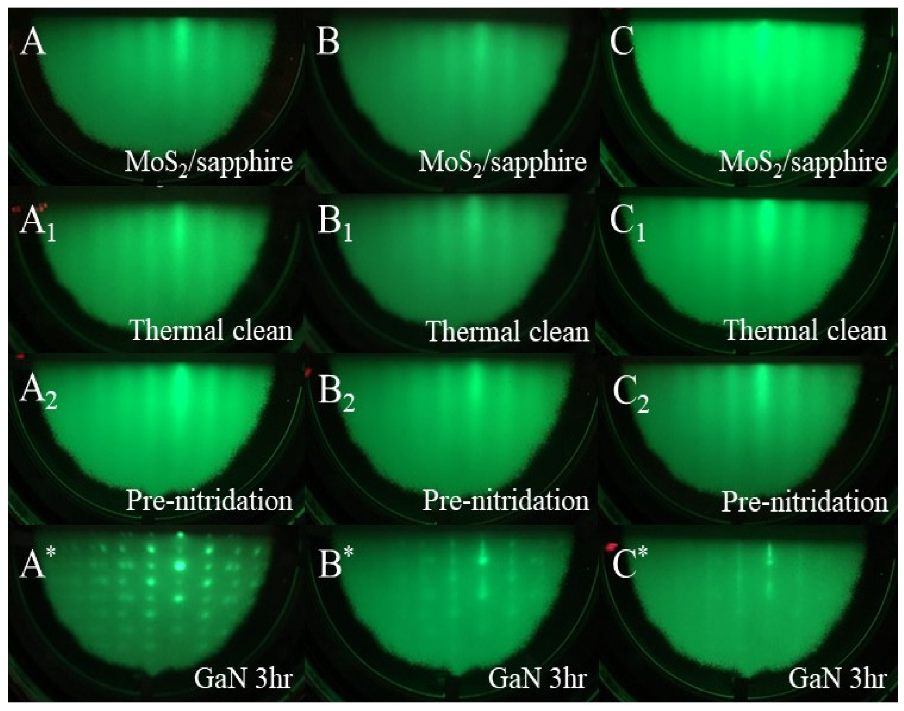
3.1. RHEED
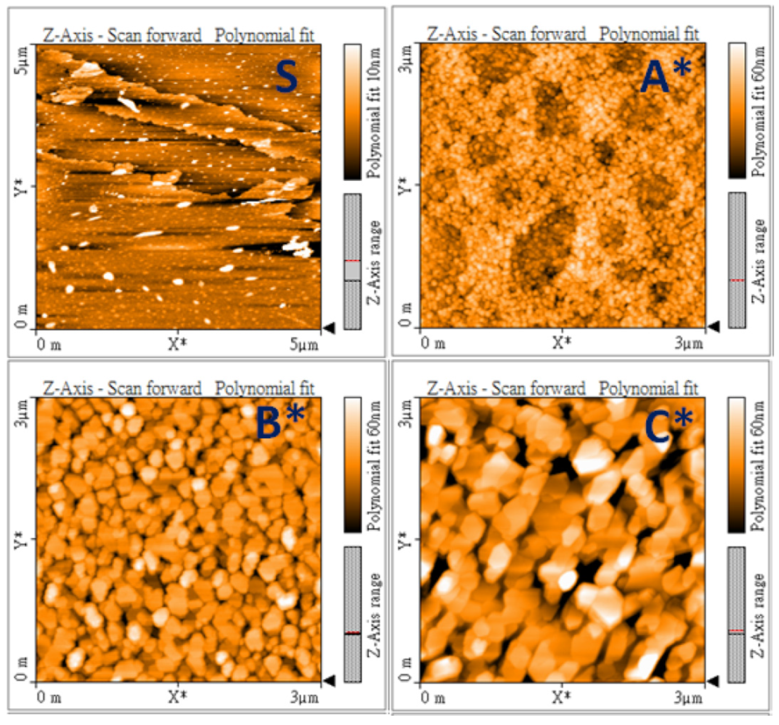
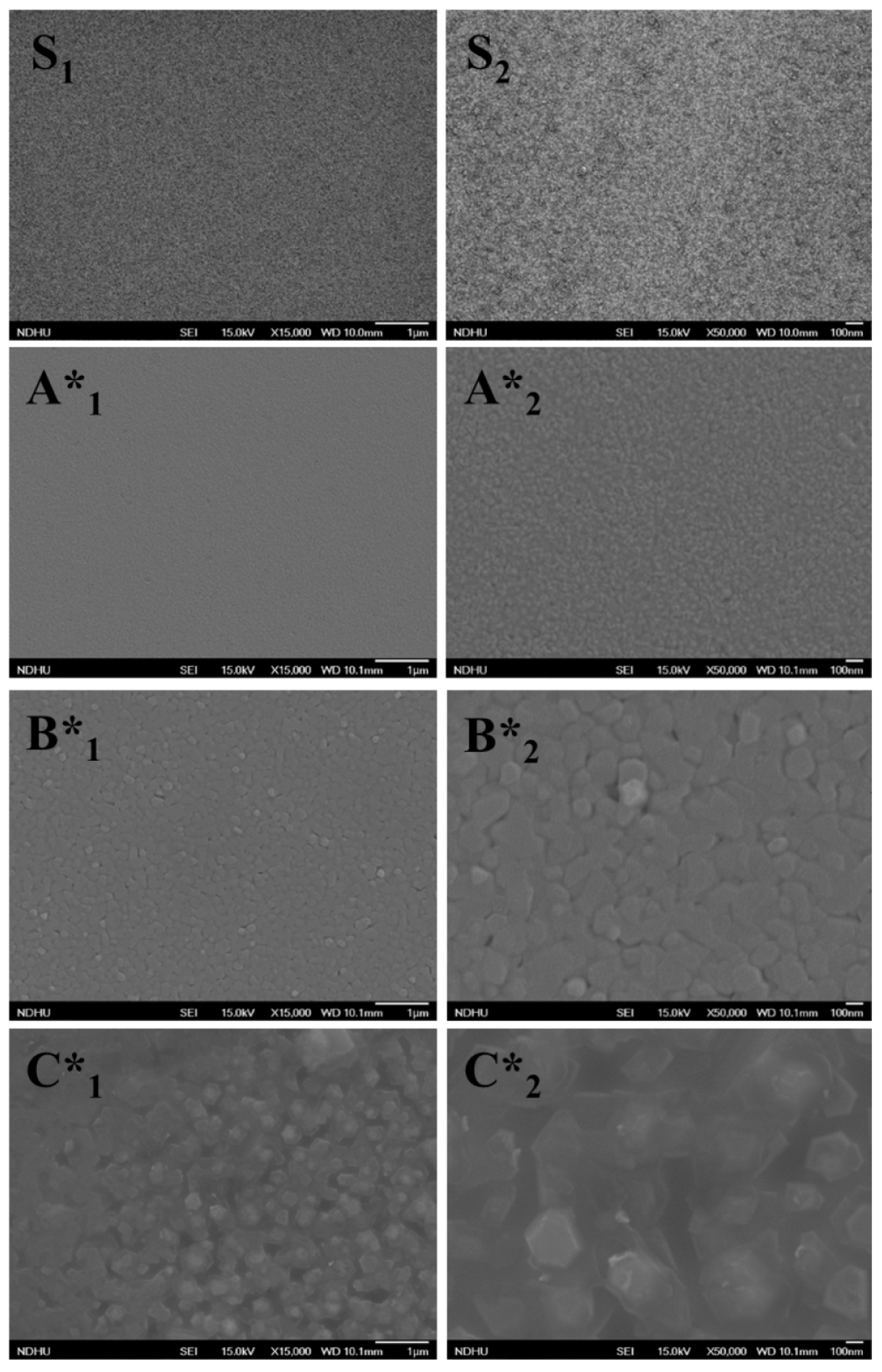
3.2. SEM
3.3. AFM
3.4. XPS
3.5. Raman
3.6. PL
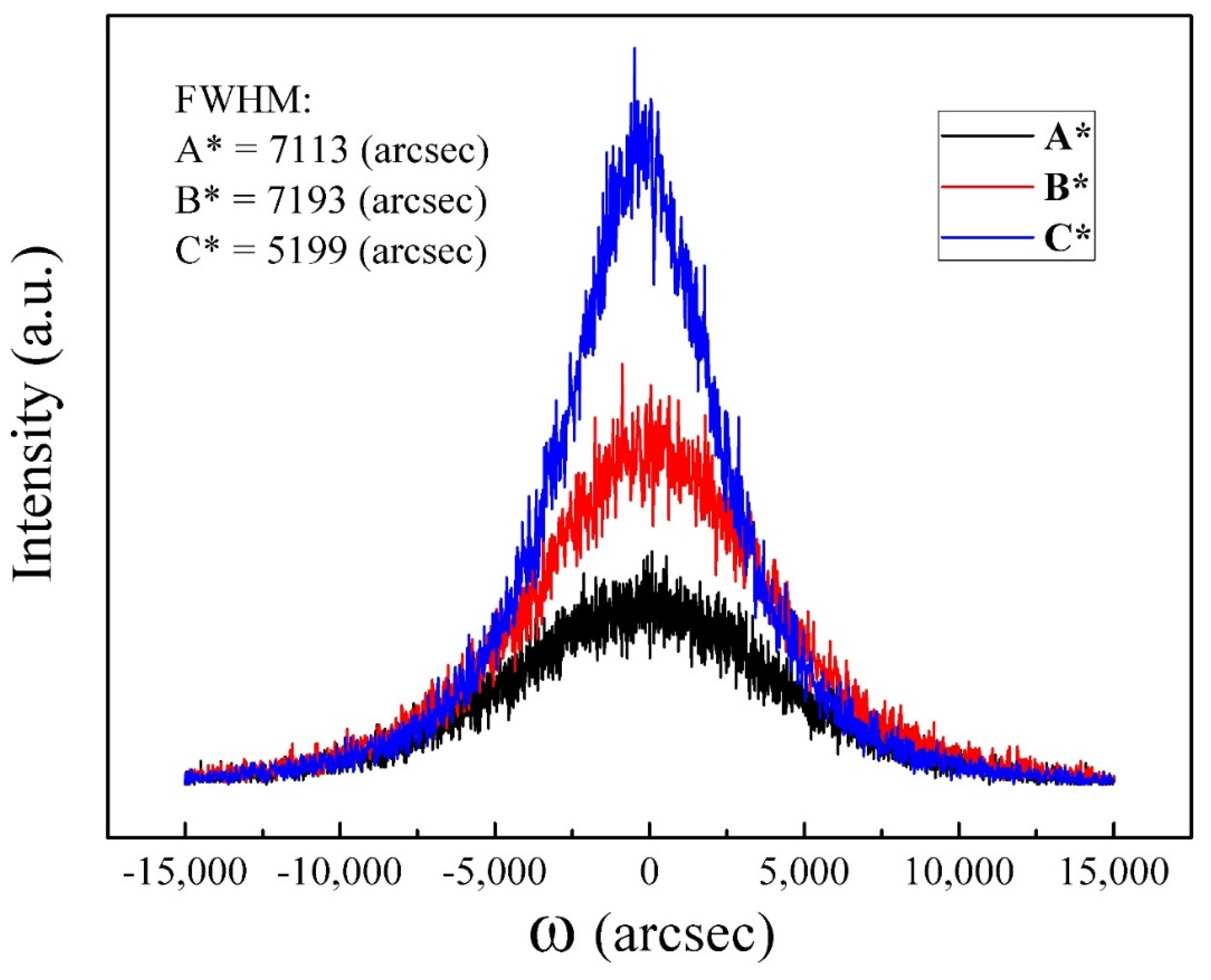
3.7. HR-XRD
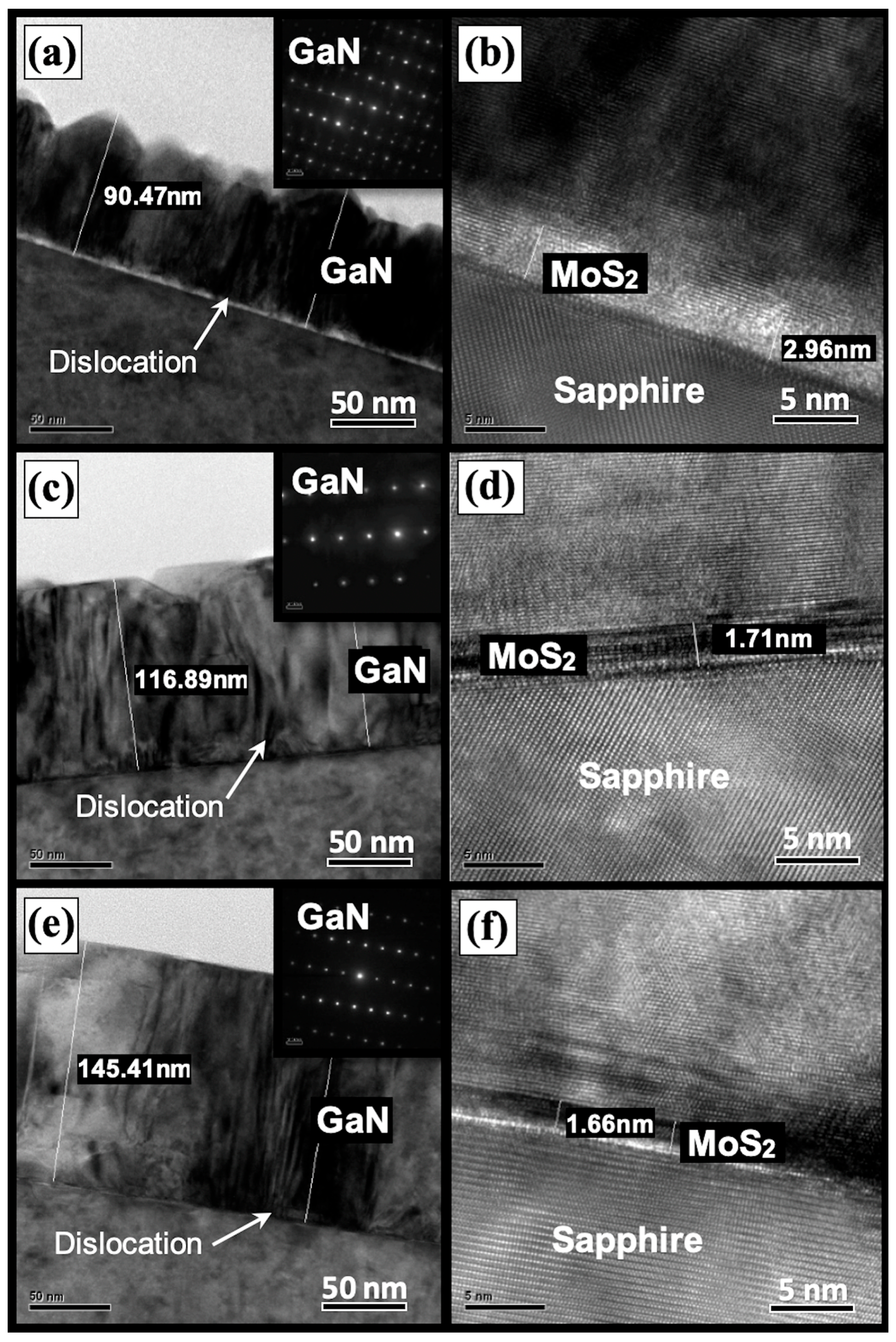
3.8. TEM
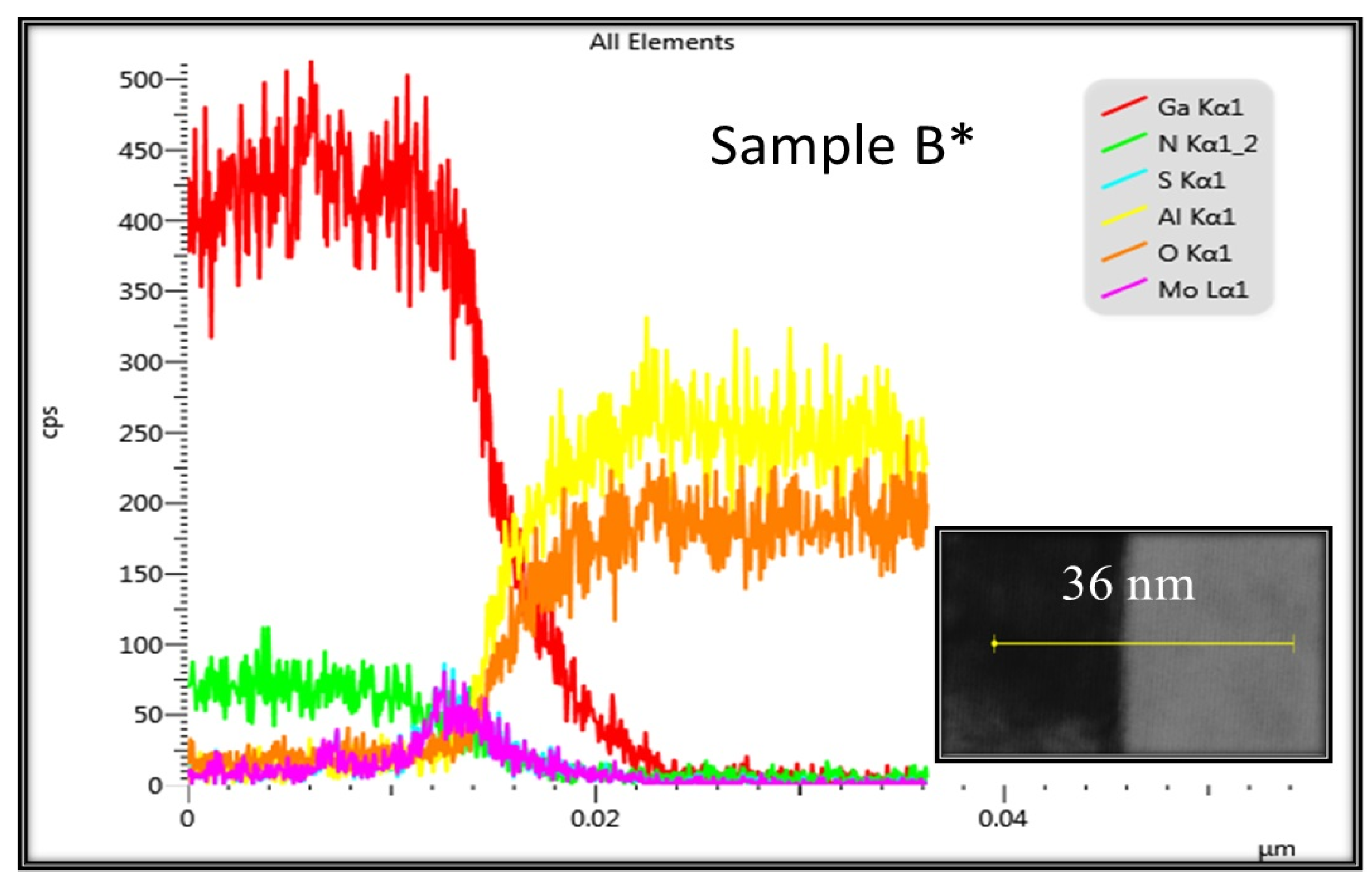
3.9. EDS
4. Conclusions
Author Contributions
Funding
Institutional Review Board Statement
Informed Consent Statement
Data Availability Statement
Acknowledgments
Conflicts of Interest
References
- Zhu, D.; Wallis, D.J.; Humphreys, C.J. Prospects of III-nitride optoelectronics grown on Si. Rep. Prog. Phys. 2013, 76, 106501. [Google Scholar] [CrossRef] [PubMed]
- Asad, M.; Li, Q.; Sachdev, M.; Wong, W.S. Thermal and optical properties of high-density GaN micro-LED arrays on flexible substrates. Nano Energy 2020, 73, 104724. [Google Scholar] [CrossRef]
- Hamza, K.H.; Nirmal, D. A review of GaN HEMT broadband power amplifiers. Int. J. Electron. Commun. 2020, 116, 153040. [Google Scholar] [CrossRef]
- Pasupuleti, K.S.; Reddeppa, M.; Park, B.-G.; Oh, J.-E.; Kim, S.-G.; Kim, M.-D. Efficient Charge Separation in Polypyrrole/GaN-NanorodBased Hybrid Heterojunctions for High-Performance Self-Powered UV Photodetection. Phys. Status Solidi RRL 2021, 15, 2000518. [Google Scholar] [CrossRef]
- Chowdhury, I.U.I.; Sarker, J.; Shifat, A.S.M.Z.; Shuvro, R.A.; Mitul, A.F. Performance analysis of high efficiency InxGa1−xN/GaN intermediate band quantum dot solar cells. Results Phys. 2018, 9, 432–439. [Google Scholar] [CrossRef]
- Xi, X.; Yang, C.; Cao, H.; Yu, Z.; Li, J.; Lin, S.; Ma, Z.; Zhao, L. GaN nanocolumns fabricated by self-assembly Ni mask and its enhanced photocatalytic performance in water splitting. Appl. Surf. Sci. 2018, 462, 310–315. [Google Scholar] [CrossRef]
- Liu, L.; Edgar, J.H. Substrates for gallium nitride epitaxy. Mater. Sci. Eng. R Rep. 2002, 37, 61–127. [Google Scholar] [CrossRef]
- Choi, W.; Choudhary, N.; Han, G.H.; Park, J.; Akinwande, D.; Lee, Y.H. Recent development of two-dimensional transition metal dichalcogenides and their applications. Mater. Today 2017, 20, 116–130. [Google Scholar] [CrossRef]
- Wong, S.L.; Liu, H.; Chi, D. Recent progress in chemical vapor deposition growth of two-dimensional transition metal dichalcogenides. Prog. Cryst. Growth Charact. Mater. 2016, 62, 9–28. [Google Scholar] [CrossRef]
- Liu, Z.; Liu, B.; Chen, Z.; Yang, S.; Liu, Z.; Wei, T.; Gao, P.; Liu, Z. Two-dimensional material-assisted remote epitaxy and van der Waals epitaxy: A review. Natl. Sci. Open 2023, 2, 20220068. [Google Scholar] [CrossRef]
- Walsh, L.A.; Hinkle, C.L. van der Waals epitaxy: 2D materials and topological insulators. Appl. Mater. Today 2017, 9, 504–515. [Google Scholar] [CrossRef]
- Roh, I.; Goh, S.H.; Meng, Y.; Kim, J.S.; Han, S.; Xu, Z.; Lee, H.E.; Kim, Y.; Bae, S.-H. Applications of remote epitaxy and van der Waals epitaxy. Nano Converg. 2023, 10, 20. [Google Scholar] [CrossRef]
- Liu, Y.; Xu, Y.; Cao, B.; Li, Z.; Zhao, E.; Yang, S.; Wang, C.; Wang, J.; Xu, K. Transferable GaN films on graphene/SiC by van der Waals epitaxy for flexible devices. Phys. Status Solidi Appl. Mater. Sci. 2019, 216, 1801027. [Google Scholar] [CrossRef]
- Giannazzo, F.; Panasci, S.E.; Schilirò, E.; Greco, G.; Roccaforte, F.; Sfuncia, G.; Nicotra, G.; Cannas, M.; Agnello, S.; Frayssinet, E.; et al. Atomic resolution interface structure and vertical current injection in highly uniform MoS2 heterojunctions with bulk GaN. Appl. Surf. Sci. 2023, 631, 157513. [Google Scholar] [CrossRef]
- Huang, C.-Y.; Chang, C.; Lu, G.-Z.; Huang, W.-C.; Huang, C.-S.; Chen, M.-L.; Lin, T.-N.; Shen, J.-L.; Lin, T.-Y. Hybrid 2D/3D MoS2/GaN heterostructures for dual functional photoresponse. Appl. Phys. Lett. 2018, 112, 23. [Google Scholar] [CrossRef]
- Krishnamoorthy, S.; Lee, E.W.; Lee, C.H.; Zhang, Y.; McCulloch, W.D.; Johnson, J.M.; Hwang, J.; Wu, Y.; Rajan, S. High current density 2D/3D MoS2/GaN Esaki tunnel diodes. Appl. Phys. Lett. 2016, 109, 18. [Google Scholar] [CrossRef]
- Ruzmetov, D.; Zhang, K.; Stan, G.; Kalanyan, B.; Bhimanapati, G.R.; Eichfeld, S.M.; Burke, R.A.; Shah, P.B.; O’Regan, T.P.; Crowne, F.J.; et al. Vertical 2D/3D semiconductor heterostructures based on epitaxial molybdenum disulfide and gallium nitride. ACS Nano 2016, 10, 3580–3588. [Google Scholar] [CrossRef] [PubMed]
- Chromik, Š.; Sojkova, M.; Vretenar, V.; Rosova, A.; Dobročka, E.; Hulman, M. Influence of GaN/AlGaN/GaN (0001) and Si (100) substrates on structural properties of extremely thin MoS2 films grown by pulsed laser deposition. Appl. Surf. Sci. 2017, 395, 232–236. [Google Scholar] [CrossRef]
- Lee, C.H.; Zhang, Y.; Johnson, J.M.; Koltun, R.; Gambin, V.; Jamison, J.S.; Myers, R.C.; Hwang, J.; Rajan, S. Molecular beam epitaxy of GaN on 2H–MoS2. Appl. Phys. Lett. 2020, 117, 123102. [Google Scholar] [CrossRef]
- Yamada, A.; Ho, K.P.; Maruyama, T.; Akimoto, K. Molecular beam epitaxy of GaN on a substrate of MoS2 layered compound. Appl. Phys. A Mater. Sci. Process. 1999, 69, 89–92. [Google Scholar] [CrossRef]
- Gupta, P.; Rahman, A.A.; Subramanian, S.; Gupta, S.; Thamizhavel, A.; Orlova, T.; Rouvimov, S.; Vishwanath, S.; Protasenko, V.; Laskar, M.R.; et al. Layered transition metal dichalcogenides: Promising near-lattice-matched substrates for GaN growth. Sci. Rep. 2015, 6, 23708. [Google Scholar] [CrossRef]
- Susanto, I.; Tsai, C.-Y.; Fachruddin; Rahmiati, T.; Ho, Y.-T.; Tsai, P.-Y.; Yu, I.-S. The influence of 2D MoS2 layers on the growth of GaN films by plasma-assisted molecular beam epitaxy. Appl. Surf. Sci. 2019, 496, 143616. [Google Scholar] [CrossRef]
- Susanto, I.; Tsai, C.-Y.; Ho, Y.-T.; Tsai, P.-Y.; Yu, I.-S. Temperature effect of van der Waals epitaxial GaN films on pulse-laser-deposited 2D MoS2 layer. Nanomaterials 2021, 11, 1406. [Google Scholar] [CrossRef] [PubMed]
- Sun, J.; Li, X.; Guo, W.; Zhao, M.; Fan, X.; Dong, Y.; Xu, C.; Deng, J.; Fu, Y. Synthesis Methods of Two-Dimensional MoS2: A Brief Review. Crystals 2017, 7, 198. [Google Scholar] [CrossRef]
- Elsass, C.R.; Poblenz, C.; Heying, B.; Fini, P.; Petroff, P.M.; Denbaars, S.P.; Mishra, U.K.; Speck, J.S. Influence of Ga flux on the growth and electron transport properties of AlGaN/GaN heterostructures grown by plasma-assisted molecular beam epitaxy. J. Cryst. Growth 2001, 233, 709–716. [Google Scholar] [CrossRef]
- Tsai, J.-K.; Lo, I.; Tu, K.-L.C.L.-W.; Huang, J.-H.; Hsieh, C.-H.; Hsieh, K.-Y. Effect of N to Ga flux ratio on the GaN surface morphologies grown at high temperature by plasma-assisted molecular-beam epitaxy. J. Appl. Phys. 2004, 95, 460–465. [Google Scholar] [CrossRef]
- Susanto, I.; Tsou, T.-H.; Yang, Z.-P.; Lee, C.-Y.; Li, H.; Yu, I.-S. Effects of N/Ga flux ratio on GaN films grown on 4H-SiC substrate with 4° miscutting orientation by plasma-assisted molecular beam epitaxy. J. Alloys Compd. 2017, 710, 800–808. [Google Scholar] [CrossRef]
- Kim, Y.; Bark, H.; Ryu, G.H.; Lee, Z.; Lee, C. Wafer-scale monolayer MoS2 grown by chemical vapor deposition using a reaction of MoO3 and H2S. J. Phys. Condens. Matter. 2016, 28, 184002. [Google Scholar] [CrossRef]
- Kumar, P.; Tuteja, M.; Kesaria, M.; Waghmare, U.V.; Shivaprasad, S.M. Superstructure of self-aligned hexagonal GaN nanorods formed on nitrided Si(111) surface. Appl. Phys. Lett. 2012, 101, 13. [Google Scholar] [CrossRef]
- Kushvaha, S.S.; Kumar, M.S.; Shukla, A.K.; Yadav, B.S.; Singh, D.K.; Jewariya, M.; Ragam, S.R.; Maurya, K.K. Structural, optical and electronic properties of homoepitaxial GaN nanowalls grown on GaN template by laser molecular beam epitaxy. RSC Adv. 2015, 5, 87818–87830. [Google Scholar] [CrossRef]
- Mishra, M.; Krishna, T.C.S.; Aggarwal, N.; Kaur, M.; Singh, S.; Gupta, G. Pit assisted oxygen chemisorption on GaN surfaces. Phys. Chem. Chem. Phys. 2015, 17, 15201–15208. [Google Scholar] [CrossRef] [PubMed]
- Tangi, M.; Mishra, P.; Ng, T.K.; Hedhili, M.N.; Janjua, B.; Alias, M.S.; Anjum, D.H.; Tseng, C.-C.; Shi, Y.; Joyce, H.J.; et al. Determination of band offsets at GaN/single-layer MoS2 heterojunction. Appl. Phys. Lett. 2016, 109, 032104. [Google Scholar] [CrossRef]
- Chakraborty, B.; Bera, A.; Muthu, D.V.S.; Bhowmick, S.; Waghmare, U.V.; Sood, A.K. Symmetry-dependent phonon renormalization in monolayer MoS2 transistor. Phys. Rev. B—Condens. Matter Mater. Phys. 2012, 85, 161403. [Google Scholar] [CrossRef]
- Ning, J.; Yan, C.; Jia, Y.; Wang, B.; Zeng, Y.; Zhang, J.; Wang, D.; Hao, Y. GaN films deposited on sapphire substrates sputter-coated with AlN followed by monolayer graphene for solid-state lighting. ACS Appl. Nano Mater. 2020, 3, 5061–5069. [Google Scholar] [CrossRef]
- Krishna, T.C.S.; Aggarwal, N.; Reddy, G.A.; Dugar, P.; Mishra, M.; Goswami, L.; Dilawar, N.; Kumar, M.; Maurya, K.K.; Gupta, G. Probing the correlation between structure, carrier dynamics and defect states of epitaxial GaN film on () sapphire grown by rf-molecular beam epitaxy. RSC Adv. 2015, 5, 73261–73267. [Google Scholar] [CrossRef]
- Krishna, S.; Aggarwal, N.; Mishra, M.; Maurya, K.K.; Singh, S.; Dilawar, N.; Nagarajan, S.; Gupta, G. Correlation of growth temperature with stress, defect states and electronic structure in an epitaxial GaN film grown on c-sapphire via plasma MBE. Phys. Chem. Chem. Phys. 2016, 18, 8005–8014. [Google Scholar] [CrossRef] [PubMed]
- Shih, H.-Y.; Shiojiri, M.; Chen, C.-H.; Yu, S.-F.; Ko, C.-T.; Yang, J.-R.; Lin, R.-M.; Chen, M.-J. Ultralow threading dislocation density in GaN epilayer on near-strain-free GaN compliant buffer layer and its applications in hetero-epitaxial LEDs. Nat. Publ. Gr. 2015, 5, 13671. [Google Scholar] [CrossRef] [PubMed]
- Lee, C.D.; Sagar, A.; Feenstra, R.M.; Inoki, C.K.; Kuan, T.S.; Sarney, W.L.; Salamanca-Riba, L. Role of Ga flux in dislocation reduction in GaN films grown on SiC(0001). Appl. Phys. Lett. 2001, 79, 3428–3430. [Google Scholar] [CrossRef]
- Moram, M.A.; Ghedia, C.S.; Rao, D.V.S.; Barnard, J.S.; Zhang, Y.; Kappers, M.J.; Humphreys, C.J. On the origin of threading dislocations in GaN films. J. Appl. Phys. 2009, 106, 073513. [Google Scholar] [CrossRef]


| Sample | A* | B* | C* |
|---|---|---|---|
| Substrate | MoS2/sapphire | ||
| Thermal cleaning | 600 °C for 30 min | ||
| Pre-nitridation | 600 °C for 10 min | ||
| Gallium K-cell temperatures | 825 °C | 875 °C | 925 °C |
| Growth temperature | 750 °C for 3 hr | ||
| Nitrogen plasma | 500 W and 0.8 sccm | ||
| Sample | A* | B* | C* |
|---|---|---|---|
| Ga-N position (eV) | 20.13 | 19.78 | 19.18 |
| Ga-Ga position (eV) | 17.8 | 17.9 | 17.4 |
| Ga-N (%) | 90.9 | 90.6 | 98.4 |
| Ga-Ga (%) | 9.1 | 9.4 | 1.6 |
Disclaimer/Publisher’s Note: The statements, opinions and data contained in all publications are solely those of the individual author(s) and contributor(s) and not of MDPI and/or the editor(s). MDPI and/or the editor(s) disclaim responsibility for any injury to people or property resulting from any ideas, methods, instructions or products referred to in the content. |
© 2024 by the authors. Licensee MDPI, Basel, Switzerland. This article is an open access article distributed under the terms and conditions of the Creative Commons Attribution (CC BY) license (https://creativecommons.org/licenses/by/4.0/).
Share and Cite
Susanto, I.; Liu, H.-S.; Ho, Y.-T.; Yu, I.-S. Epitaxial Growth of GaN Films on Chemical-Vapor-Deposited 2D MoS2 Layers by Plasma-Assisted Molecular Beam Epitaxy. Nanomaterials 2024, 14, 732. https://doi.org/10.3390/nano14080732
Susanto I, Liu H-S, Ho Y-T, Yu I-S. Epitaxial Growth of GaN Films on Chemical-Vapor-Deposited 2D MoS2 Layers by Plasma-Assisted Molecular Beam Epitaxy. Nanomaterials. 2024; 14(8):732. https://doi.org/10.3390/nano14080732
Chicago/Turabian StyleSusanto, Iwan, Hong-Shan Liu, Yen-Ten Ho, and Ing-Song Yu. 2024. "Epitaxial Growth of GaN Films on Chemical-Vapor-Deposited 2D MoS2 Layers by Plasma-Assisted Molecular Beam Epitaxy" Nanomaterials 14, no. 8: 732. https://doi.org/10.3390/nano14080732
APA StyleSusanto, I., Liu, H.-S., Ho, Y.-T., & Yu, I.-S. (2024). Epitaxial Growth of GaN Films on Chemical-Vapor-Deposited 2D MoS2 Layers by Plasma-Assisted Molecular Beam Epitaxy. Nanomaterials, 14(8), 732. https://doi.org/10.3390/nano14080732