

Electrodeposition of Nanostructured Metals on n-Silicon and Insights into Rhodium Deposition

 , ,
, ,  , ,
, ,  and
and 
Abstract
1. Introduction
2. Materials and Methods
2.1. Reagents
2.2. Experimental Setup
3. Results and Discussion
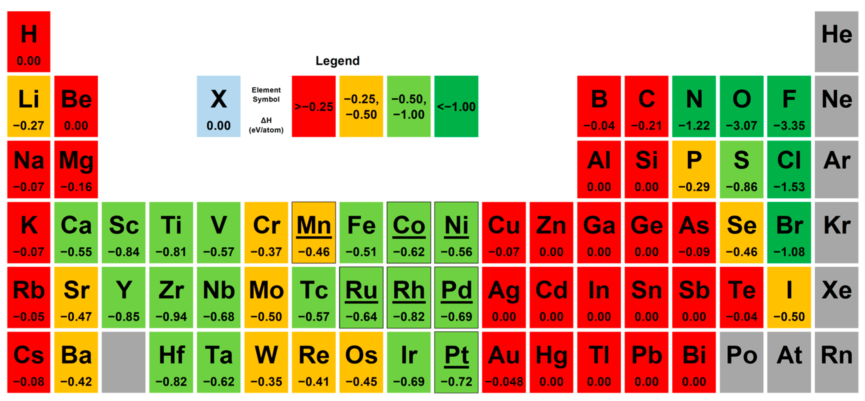
3.1. Metals’ Selection
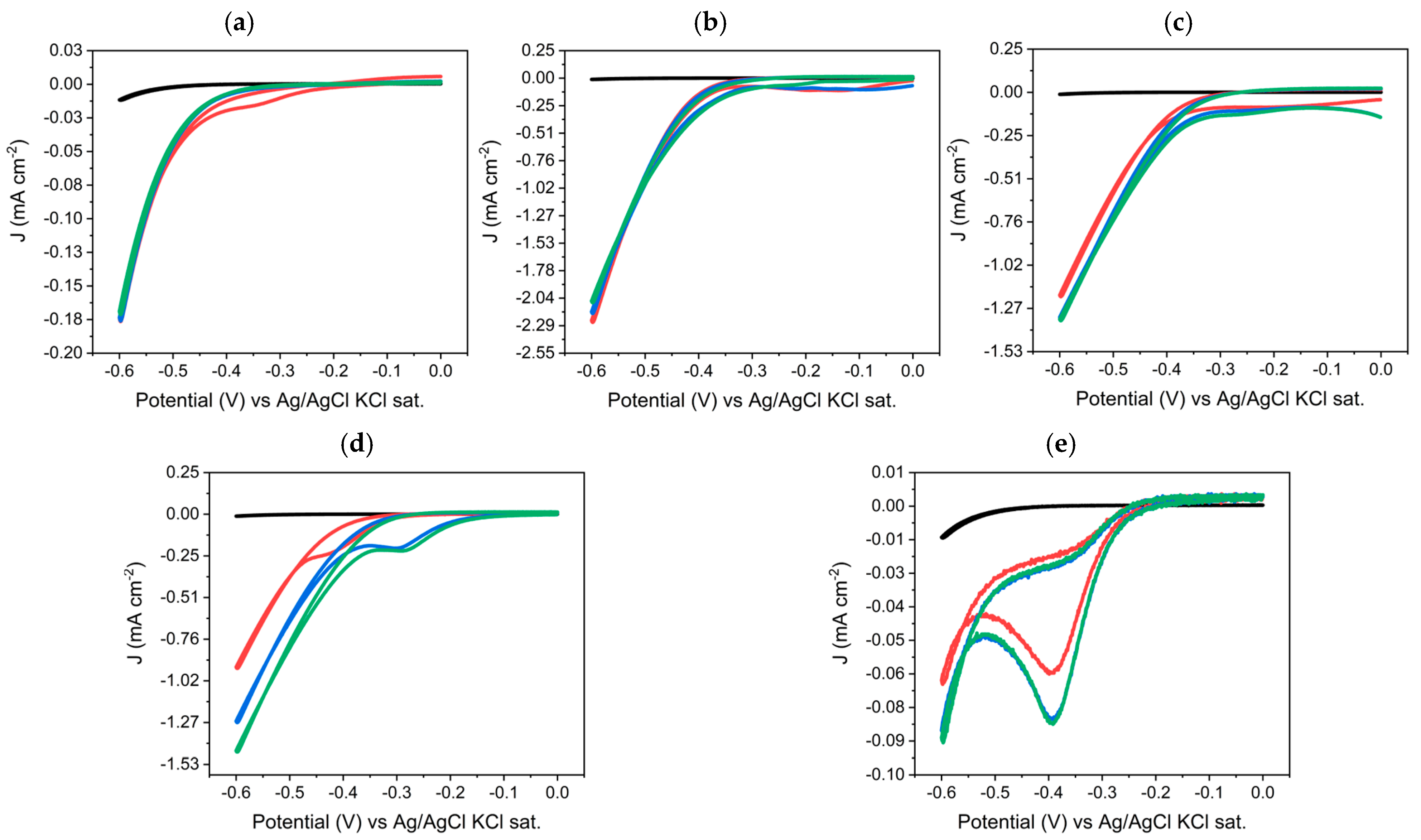
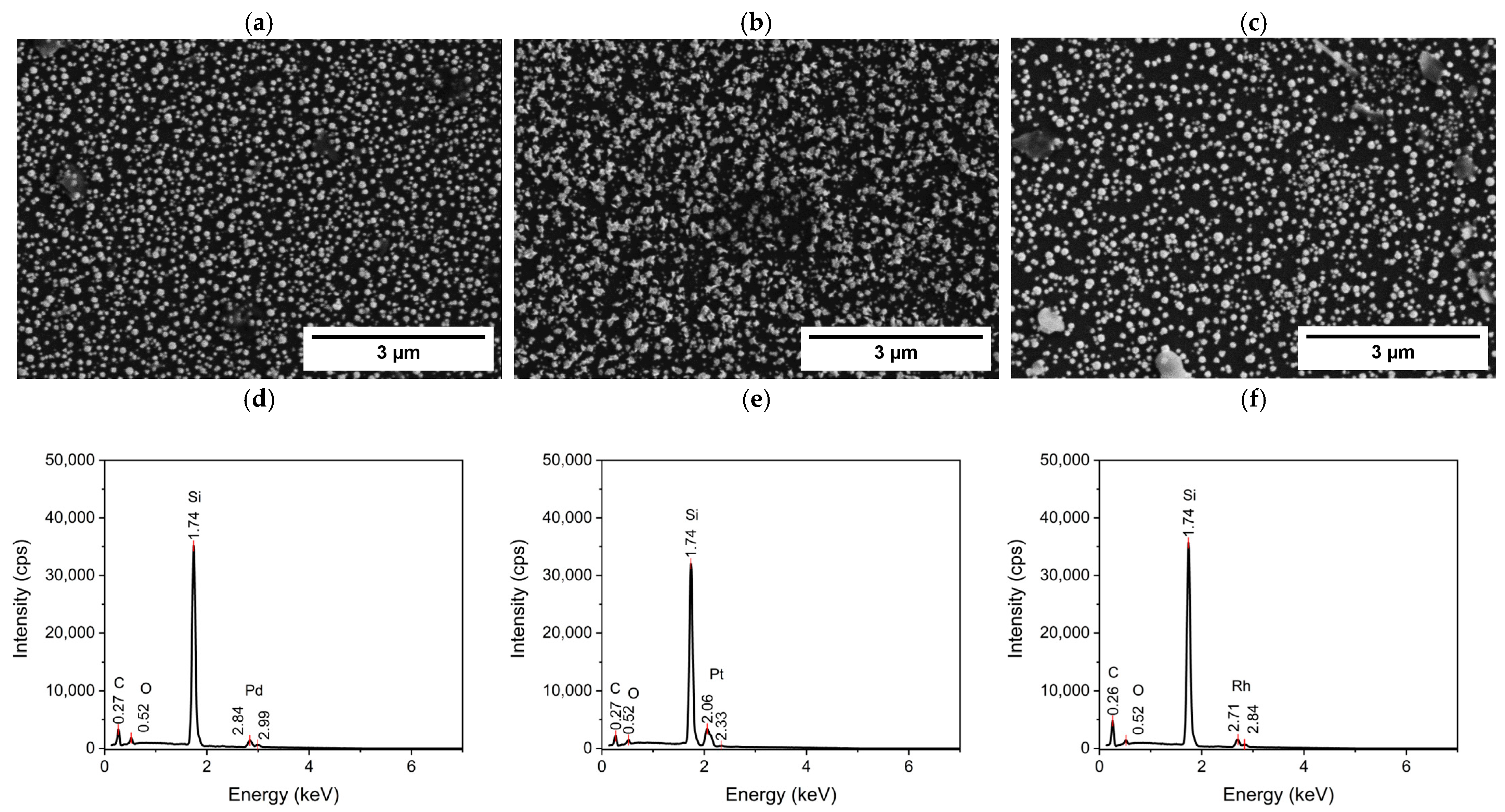
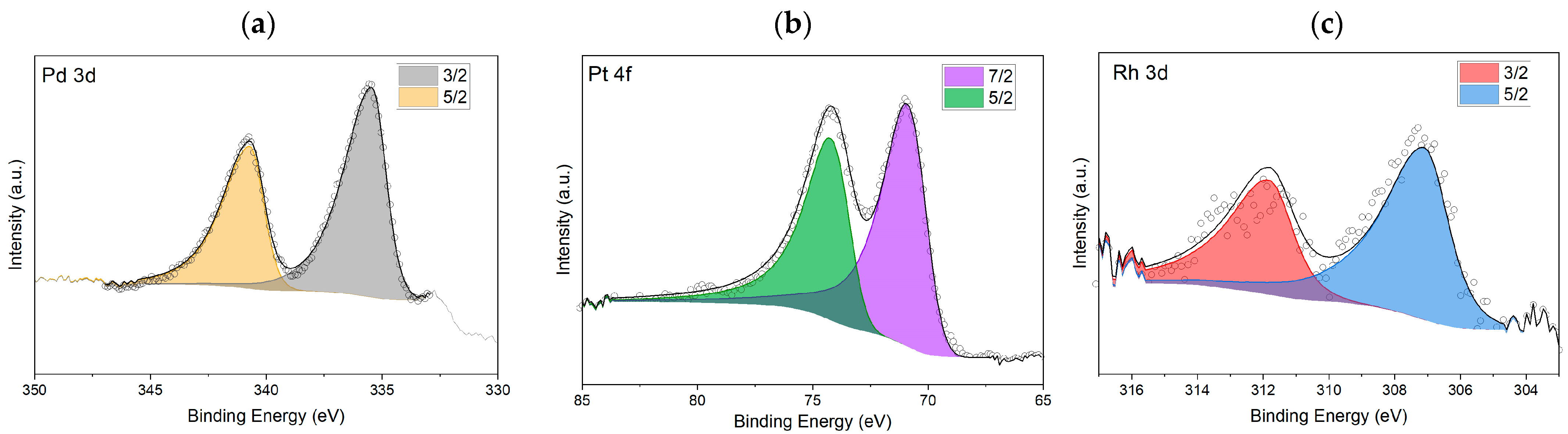
3.2. Cyclic Voltammetry Measurements and Characterization
3.3. Charge-Controlled Deposition
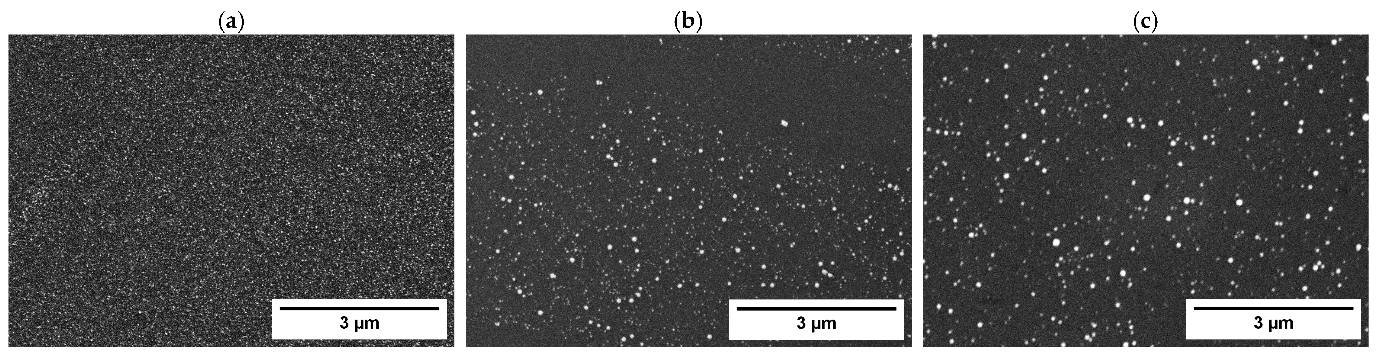
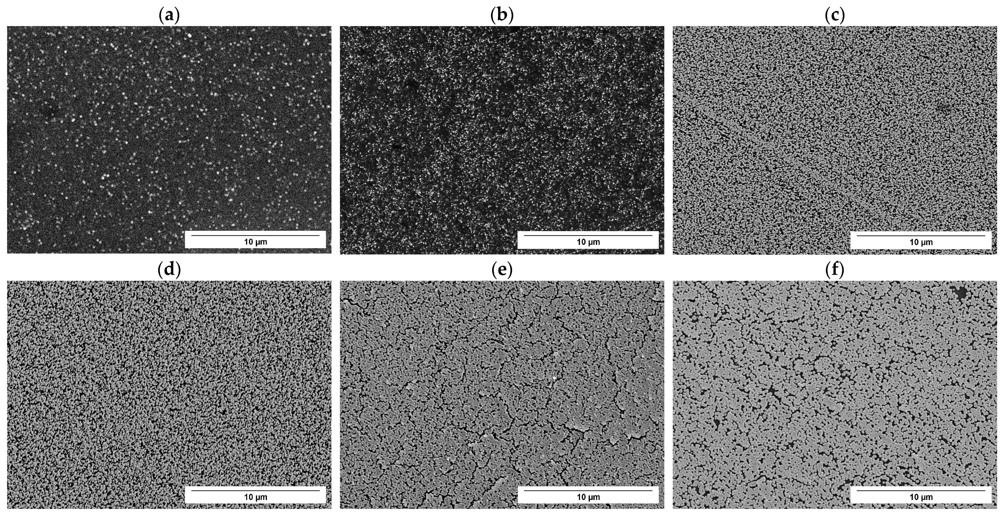
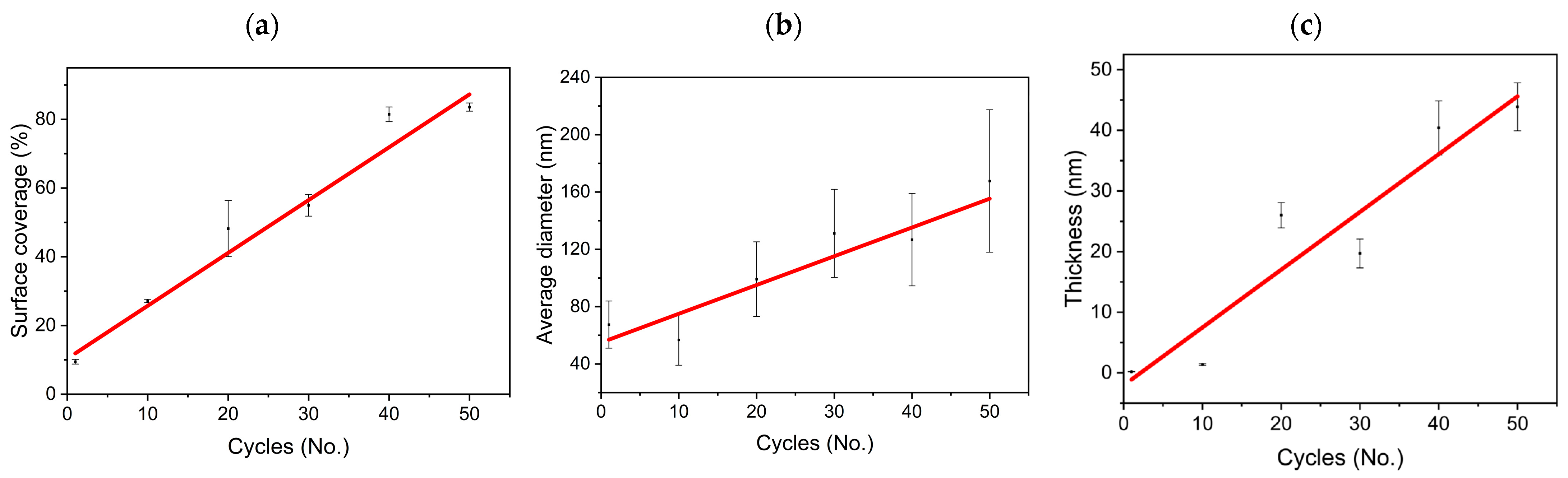
3.4. Multi-Cycle Charge-Controlled Deposition
4. Conclusions
Supplementary Materials
Author Contributions
Funding
Data Availability Statement
Conflicts of Interest
References
- Sulka, G.D. Electrochemistry of Thin Films and Nanostructured Materials. Molecules 2023, 28, 4040. [Google Scholar] [CrossRef] [PubMed]
- Fukata, N.; Subramani, T.; Jevasuwan, W.; Dutta, M.; Bando, Y. Functionalization of Silicon Nanostructures for Energy-Related Applications. Small 2017, 13, 1701713. [Google Scholar] [CrossRef]
- Kuntyi, O.I.; Zozulya, G.I.; Shepida, M.V.; Nichkalo, S.I. Deposition of Nanostructured Metals on the Surface of Silicon by Galvanic Replacement: A Mini-Review. Vopr. Khimii Khimicheskoi Tekhnologii 2019, 2019, 74–82. [Google Scholar] [CrossRef]
- Azzaroni, O.; Fonticelli, M.; Schilardi, P.L.; Benítez, G.; Caretti, I.; Albella, J.M.; Gago, R.; Vázquez, L.; Salvarezza, R.C. Surface Nanopatterning of Metal Thin Films by Physical Vapour Deposition onto Surface-Modified Silicon Nanodots. Nanotechnology 2004, 15, S197–S200. [Google Scholar] [CrossRef]
- Abo Ghazala, M.S.; Othman, H.A.; Sharaf El-Deen, L.M.; Nawwar, M.A.; Kashyout, A.E.H.B. Fabrication of Nanocrystalline Silicon Thin Films Utilized for Optoelectronic Devices Prepared by Thermal Vacuum Evaporation. ACS Omega 2020, 5, 27633–27644. [Google Scholar] [CrossRef]
- Droopad, R.; Curless, J.A.; Yu, Z.; Jordan, D.C.; Liang, Y.; Overgaard, C.D.; Li, H.; Eschrich, T.; Craigo, B.; Eisenbeiser, K.W.; et al. Development of Integrated Heterostructures on Silicon by MBE. In Proceedings of the MBE 2002—2002 12th International Conference on Molecular Bean Epitaxy, San Francisco, CA, USA, 15–20 September 2002; Volume 251, pp. 45–46. [Google Scholar] [CrossRef]
- Sarkar, J. Sputtering Materials for VLSI and Thin Film Devices, 1st ed.; Elsevier: Amsterdam, The Netherlands, 2000; ISBN 9780080947716. [Google Scholar]
- Thomann, A.L.; Vahlas, C.; Aloui, L.; Samelor, D.; Caillard, A.; Shaharil, N.; Blanc, R.; Millon, E. Conformity of Aluminum Thin Films Deposited onto Micro-Patterned Silicon Wafers by Pulsed Laser Deposition, Magnetron Sputtering, and CVD. Chem. Vap. Depos. 2011, 17, 366–374. [Google Scholar] [CrossRef]
- Mitzi, D.B.; Kosbar, L.L.; Murray, C.E.; Copel, M.; Afzali, A. High-Mobility Ultrathin Semiconducting Films Prepared by Spin Coating. Nature 2004, 428, 299–303. [Google Scholar] [CrossRef]
- Srinivasan, K.; Kottantharayil, A. Aluminium Oxide Thin Film Deposited by Spray Coating for P-Type Silicon Surface Passivation. Sol. Energy Mater. Sol. Cells 2019, 197, 93–98. [Google Scholar] [CrossRef]
- Pasa, A.A.; Schwarzacher, W. Electrodeposition of Thin Films and Multilayers on Silicon. Phys. Status Solidi Appl. Res. 1999, 173, 73–84. [Google Scholar] [CrossRef]
- Pappaianni, G.; Giurlani, W.; Bonechi, M.; Calisi, N.; Cortigiani, B.; Bazzicalupi, C.; Caneschi, A.; Fontanesi, C.; Innocenti, M. Electrodeposition of MnAs-Based Thin-Film as a Possible Promising Candidate in Spintronics Applications. J. Electrochem. Soc. 2024, 171, 062502. [Google Scholar] [CrossRef]
- Foresti, M.L.; Milani, S.; Loglio, F.; Innocenti, M.; Pezzatini, G.; Cattarin, S. Ternary CdSxSe1-x Deposited on Ag(111) by ECALE: Synthesis and Characterization. Langmuir 2005, 21, 6900–6907. [Google Scholar] [CrossRef] [PubMed]
- Giurlani, W.; Giaccherini, A.; Calisi, N.; Zangari, G.; Salvietti, E.; Passaponti, M.; Caporali, S. Investigations on the Electrochemical Atomic Layer Growth of Bi2Se3 and the Surface Limited Deposition of Bismuth at the Silver Electrode. Materials 2018, 11, 1426. [Google Scholar] [CrossRef]
- Giurlani, W.; Giaccherini, A.; Salvietti, E.; Passaponti, M.; Comparini, A.; Morandi, V.; Liscio, F.; Cavallini, M.; Innocenti, M. Selective Electrodesorption-Based Atomic Layer Deposition (SEBALD) of Bismuth under Morphological Control. Electrochem. Soc. Interface 2018, 27, 77–81. [Google Scholar] [CrossRef]
- Giurlani, W.; Cavallini, M.; Picca, R.A.; Cioffi, N.; Passaponti, M.; Fontanesi, C.; Lavacchi, A.; Innocenti, M. Underpotential-Assisted Electrodeposition of Highly Crystalline and Smooth Thin Film of Bismuth. ChemElectroChem 2020, 7, 299–305. [Google Scholar] [CrossRef]
- Gregory, B.W.; Stickney, J.L. Electrochemical Atomic Layer Epitaxy (ECALE). J. Electroanal. Chem. 1991, 300, 543–561. [Google Scholar] [CrossRef]
- Vizza, M.; Giaccherini, A.; Giurlani, W.; Passaponti, M.; Cioffi, N.; Picca, R.A.; De Luca, A.; Fabbri, L.; Lavacchi, A.; Gambinossi, F.; et al. Successes and Issues in the Growth of Moad and MoSe2 on Ag(111) by the E-ALD Method. Metals 2019, 9, 122. [Google Scholar] [CrossRef]
- Ogata, Y.H.; Kobayashi, K.; Motoyama, M. Electrochemical Metal Deposition on Silicon. Curr. Opin. Solid State Mater. Sci. 2006, 10, 163–172. [Google Scholar] [CrossRef]
- Zhang, X.G. Electrochemistry of Silicon and Its Oxide; Springer: New York, NY, USA, 2001; ISBN 9780306465413. [Google Scholar]
- Electrical & Computer Engineering, Integrated Microfabrication Lab, Brigham Young University. Metal-Semiconductor Ohmic and Schottky Contacts. Available online: https://cleanroom.byu.edu/ohmic-schottky (accessed on 4 December 2023).
- Tung, R.T. Recent Advances in Schottky Barrier Concepts. Mater. Sci. Eng. R Reports 2001, 35, 1–138. [Google Scholar] [CrossRef]
- Sato, N. Electrocthemistry of Semiconductors. Tetsu-to-Hagane 1990, 76, 1423–1436. [Google Scholar] [CrossRef] [PubMed]
- Oskam, G.; Long, J.G.; Natarajan, A.; Searson, P.C. Electrochemical Deposition of Metals onto Silicon. J. Phys. D Appl. Phys. 1998, 31, 1927. [Google Scholar] [CrossRef]
- Giurlani, W.; Dell’Aquila, V.; Vizza, M.; Calisi, N.; Lavacchi, A.; Irrera, A.; Lo Faro, M.J.; Leonardi, A.A.; Morganti, D.; Innocenti, M. Electrodeposition of Nanoparticles and Continuous Film of CdSe on N-Si (100). Nanomaterials 2019, 9, 1504. [Google Scholar] [CrossRef] [PubMed]
- Giurlani, W.; Vizza, M.; Leonardi, A.A.; Lo Faro, M.J.; Irrera, A.; Innocenti, M. Optimization and Characterization of Electrodeposited Cadmium Selenide on Monocrystalline Silicon. Nanomaterials 2022, 12, 610. [Google Scholar] [CrossRef]
- Prod’Homme, P.; Maroun, F.; Cortès, R.; Allongue, P. Electrochemical Growth of Ultraflat Au(111) Epitaxial Buffer Layers on H-Si(111). Appl. Phys. Lett. 2008, 93, 171901. [Google Scholar] [CrossRef]
- Skachkov, D.; Liu, S.; Wang, Y.; Zhang, X.; Cheng, H. First-Principles Theory for Schottky Barrier Physics. Phys. Rev. B 2021, 104, 045429. [Google Scholar] [CrossRef]
- Muñoz, A.G. Electroplating of Rhodium/Si(111) Junctions for Solar Fuel Generation: Effects of Hydrogen Diffusion. J. Electrochem. Soc. 2014, 161, D571–D578. [Google Scholar] [CrossRef]
- Wasilewska, J.; Chmielarek, M.; Skupiński, W. Study of Rh/TiO2–SiO2 System in Photolytic Water Splitting. React. Kinet. Mech. Catal. 2021, 132, 1165–1192. [Google Scholar] [CrossRef]
- Dang, Q.; Liao, F.; Sun, Y.; Zhang, S.; Huang, H.; Shen, W.; Kang, Z.; Shi, Y.; Shao, M. Rhodium/Silicon Quantum Dot/Carbon Quantum Dot Composites as Highly Efficient Electrocatalysts for Hydrogen Evolution Reaction with Pt-like Performance. Electrochim. Acta 2019, 299, 828–834. [Google Scholar] [CrossRef]
- Song, Z.; Chang, H.; Zhu, W.; Xu, C.; Feng, X. Rhodium Nanoparticle-Mesoporous Silicon Nanowire Nanohybrids for Hydrogen Peroxide Detection with High Selectivity. Sci. Rep. 2015, 5, 7792. [Google Scholar] [CrossRef]
- Marot, L.; Schoch, R.; Steiner, R.; Thommen, V.; Mathys, D.; Meyer, E. Rhodium and Silicon System: II. Rhodium Silicide Formation. Nanotechnology 2010, 21, 365707. [Google Scholar] [CrossRef]
- Grätzel, M. Highly Efficient Nanocrystalline Photovoltaic Devices. Platin. Met. Rev. 1994, 38, 151–159. [Google Scholar] [CrossRef]
- Pillai, S.; Catchpole, K.R.; Trupke, T.; Zhang, G.; Zhao, J.; Green, M.A. Enhanced Emission from Si-Based Light-Emitting Diodes Using Surface Plasmons. Appl. Phys. Lett. 2006, 88, 161102. [Google Scholar] [CrossRef]
- Wang, F.; Chen, G.; Zhang, N.; Liu, X.; Ma, R. Engineering of Carbon and Other Protective Coating Layers for Stabilizing Silicon Anode Materials. Carbon Energy 2019, 1, 219–245. [Google Scholar] [CrossRef]
- Feng, L.; Zhang, M.; Wang, J.; Zhou, X.; Qiang, X.; Guo, G.; Ren, X. Silicon Photonic Devices for Scalable Quantum Information Applications. Photonics Res. 2022, 10, A135. [Google Scholar] [CrossRef]
- Yalavarthi, R.; Yesilyurt, O.; Henrotte, O.; Kment, Š.; Shalaev, V.M.; Boltasseva, A.; Naldoni, A. Multimetallic Metasurfaces for Enhanced Electrocatalytic Oxidations in Direct Alcohol Fuel Cells. Laser Photonics Rev. 2022, 16, 2200137. [Google Scholar] [CrossRef]
- Ullah, A.; Wang, Y.-C.; Yeasmin, S.; Deng, Y.; Ren, J.; Shi, Y.; Liu, L.; Cheng, L.-J. Reconfigurable Photoinduced Terahertz Wave Modulation Using Hybrid Metal–Silicon Metasurface. Opt. Lett. 2022, 47, 2750. [Google Scholar] [CrossRef]
- Kern, W. Evolution of Silicon Wafer Cleaning Technology. Proc.-Electrochem. Soc. 1990, 90, 3–19. [Google Scholar] [CrossRef]
- Tian, F.; Yang, D.; Opila, R.L.; Teplyakov, A. V Applied Surface Science Chemical and Electrical Passivation of Si(111) Surfaces. Appl. Surf. Sci. 2012, 258, 3019–3026. [Google Scholar] [CrossRef]
- Innocenti, M.; Pezzatini, G.; Forni, F.; Foresti, M.L. CdS and ZnS Deposition on Ag(111) by Electrochemical Atomic Layer Epitaxy. J. Electrochem. Soc. 2001, 148, C357. [Google Scholar] [CrossRef]
- Shirley, D.A. High-Resolution X-Ray Photoemission Spectrum of the Valence Bands of Gold. Phys. Rev. B 1972, 5, 4709–4714. [Google Scholar] [CrossRef]
- X-Ray Photoelectron Spectroscopy (XPS) Reference Pages. Available online: http://www.xpsfitting.com/search/label/carbon (accessed on 10 January 2024).
- Susi, T.; Pichler, T.; Ayala, P. X-Ray Photoelectron Spectroscopy of Graphitic Carbon Nanomaterials Doped with Heteroatoms. Beilstein J. Nanotechnol. 2015, 6, 177–192. [Google Scholar] [CrossRef] [PubMed]
- Moulder, J.; Stickle, W.; Sobol, P.; Kenneth, B. Handbook of X-Ray Photoelectron Spectroscopy; Perkin-Elmer Corporation. Physical Electronics Division: Eden Prairie, MN, USA, 1992; ISBN 0962702625. [Google Scholar]
- Chris, W. The Open Quantum Materials Database. Available online: https://oqmd.org/ (accessed on 15 November 2023).
- Kirklin, S.; Saal, J.E.; Meredig, B.; Thompson, A.; Doak, J.W.; Aykol, M.; Rühl, S.; Wolverton, C. The Open Quantum Materials Database (OQMD): Assessing the Accuracy of DFT Formation Energies. npj Comput. Mater. 2015, 1, 15010. [Google Scholar] [CrossRef]
- Saal, J.E.; Kirklin, S.; Aykol, M.; Meredig, B.; Wolverton, C. Materials Design and Discovery with High-Throughput Density Functional Theory: The Open Quantum Materials Database (OQMD). JOM 2013, 65, 1501–1509. [Google Scholar] [CrossRef]
- Agrawal, A.; Jha, D.; Paul, A.; Liao, W.-K.; Choundhary, A. Formation Energy Predictor. Available online: http://info.eecs.northwestern.edu/ (accessed on 15 November 2023).
- Jha, D.; Ward, L.; Paul, A.; Liao, W.K.; Choudhary, A.; Wolverton, C.; Agrawal, A. ElemNet: Deep Learning the Chemistry of Materials From Only Elemental Composition. Sci. Rep. 2018, 8, 17593. [Google Scholar] [CrossRef]
- Agrawal, A.; Meredig, B.; Wolverton, C.; Choudhary, A. A Formation Energy Predictor for Crystalline Materials Using Ensemble Data Mining. In Proceedings of the 2016 IEEE 16th International Conference on Data Mining Workshops (ICDMW), Barcelona, Spain, 12–15 December 2016; pp. 1276–1279. [Google Scholar] [CrossRef]
- Meredig, B.; Agrawal, A.; Kirklin, S.; Saal, J.E.; Doak, J.W.; Thompson, A.; Zhang, K.; Choudhary, A.; Wolverton, C. Combinatorial Screening for New Materials in Unconstrained Composition Space with Machine Learning. Phys. Rev. B-Condens. Matter Mater. Phys. 2014, 89, 094104. [Google Scholar] [CrossRef]
- Jain, A.; Ong, S.P.; Hautier, G.; Chen, W.; Richards, W.D.; Dacek, S.; Jain, A.; Ong, P.; Hautier, G.; Chen, W.; et al. Commentary: The Materials Project: A Materials Genome. APL Mater. 2013, 1, 011002. [Google Scholar] [CrossRef]
- Pourbaix, M. Atlas of Electrochemical Equilibria in Aqueous Solutions. In Natl. Assoc. Corros. Eng. Cent. Beige d’Etude Corros. CEBELCOR; NACE: Brussels, Belgium, 1974; ISBN 0915567989. [Google Scholar]
- Palmstrøm, C.J. Contacts for Compound Semiconductors: Ohmic Type. In Encyclopedia of Materials: Science and Technology, 2nd ed.; Elsevier: Amsterdam, The Netherlands, 2001; pp. 1581–1587. [Google Scholar] [CrossRef]
- Tu, K.N.; Thompson, R.D.; Tsaur, B.Y.; Tu, K.N.; Thompson, R.D.; Tsaur, B.Y. Low Schottky Barrier of Rareearth Silicide on NSi. Appl. Phys. Lett. 1981, 626, 6–9. [Google Scholar] [CrossRef]
- Herrero, E.; Buller, L.J.; Abruna, D. Underpotential Deposition at Single Crystal Surfaces of Au, Pt, Ag and Other Materials. Chem. Rev. 2001, 101, 1897–1930. [Google Scholar] [CrossRef]
- Sarkar, S.; Sebastian, P.C. Inorganic Chemistry. Inorg. Chem. Front. 2018, 2018, 9. [Google Scholar] [CrossRef]
- Cheng, N.; Stambula, S.; Wang, D.; Banis, M.N.; Liu, J.; Riese, A.; Xiao, B.; Li, R.; Sham, T.; Liu, L.; et al. Hydrogen Evolution Reaction. Nat. Commun. 2016, 7, 13638. [Google Scholar] [CrossRef]
- Zhu, L.; Lin, H.; Li, Y.; Liao, F.; Lifshitz, Y.; Sheng, M.; Lee, S. A Rhodium/Silicon Co-Electrocatalyst Design Concept to Surpass Platinum Hydrogen Evolution Activity at High Overpotentials. Nat. Commun. 2016, 7, 12272. [Google Scholar] [CrossRef]
- Lee, J.; Arrigan, D.W.M.; Silvester, D.S. Mechanical Polishing as an Improved Surface Treatment for Platinum Screen-Printed Electrodes. Sens. Bio-Sensing Res. 2016, 9, 38–44. [Google Scholar] [CrossRef]
- Michaelson, H.B. The Work Function of the Elements and Its Periodicity. J. Appl. Phys. 1977, 48, 4729–4733. [Google Scholar] [CrossRef]
- Tumelero, M.A.; Benetti, L.C.; Isoppo, E.; Faccio, R.; Zangari, G.; Pasa, A.A. Electrodeposition and Ab Initio Studies of Metastable Orthorhombic Bi2Se3: A Novel Semiconductor with Bandgap for Photovoltaic Applications. J. Phys. Chem. C 2016, 120, 11797–11806. [Google Scholar] [CrossRef]
- Lattice Constants for All the Elements in the Periodic Table. Available online: https://periodictable.com/Properties/A/LatticeConstants.html (accessed on 20 December 2023).
- Philipsen, H.; Jehoul, H.; Inoue, F.; Vandersmissen, K.; Yang, L.; Struyf, H.; van Dorp, D. Nucleation and Growth Kinetics of Electrodeposited Ni Films on Si(100) Surfaces. Electrochim. Acta 2017, 230, 407–417. [Google Scholar] [CrossRef]
- Philipsen, H.; Monnens, W. Immersion and Electrochemical Deposition of Ru on Si. Electrochim. Acta 2018, 274, 306–315. [Google Scholar] [CrossRef]
- Palladium, X-Ray Photoelectron Spectroscopy (XPS) Reference Pages. Available online: http://www.xpsfitting.com/2017/10/palladium.html (accessed on 10 January 2024).
- Platinum, X-Ray Photoelectron Spectroscopy (XPS) Reference Pages. Available online: http://www.xpsfitting.com/2012/01/platinum.html (accessed on 10 January 2024).
- Rhodium, X-Ray Photoelectron Spectroscopy (XPS) Reference Pages. Available online: http://www.xpsfitting.com/2016/12/rhodium.html (accessed on 10 January 2024).
- Kreyling, W.G.; Semmler-Behnke, M.; Chaudhry, Q. A Complementary Definition of Nanomaterial. Nanotoday 2010, 5, 165–168. [Google Scholar] [CrossRef]
- Kuznetsov, G.V.; Skryshevsky, V.A.; Vdovenkova, T.A.; Tsyganova, A.I.; Gorostiza, P.; Sanz, F. Platinum Electroless Deposition on Silicon from Hydrogen Fluoride Solutions: Electrical Properties. J. Electrochem. Soc. 2001, 148, C528. [Google Scholar] [CrossRef]

| Oxidation Number of the Metal in the Salt | Metal/Silicon Most Stable Stoichiometry | Number of Electrons Exchanged | Charge (µC) | Peak Potential | |
|---|---|---|---|---|---|
| Rh | 3+ | 1:1 | 3 | 256 + 15% | −0.425 V |
| Pt | 2+ | 1:2 | 4 | 341 + 15% | −0.150 V |
| Pd | 2+ | 1:2 | 4 | 341 + 15% | −0.170 V |
| Ru | 3+ | 1:1 | 3 | 256 + 15% | −0.400 V |
| Ni | 2+ | 1:2 | 4 | 341 + 15% | −0.375 V |
Disclaimer/Publisher’s Note: The statements, opinions and data contained in all publications are solely those of the individual author(s) and contributor(s) and not of MDPI and/or the editor(s). MDPI and/or the editor(s) disclaim responsibility for any injury to people or property resulting from any ideas, methods, instructions or products referred to in the content. |
© 2024 by the authors. Licensee MDPI, Basel, Switzerland. This article is an open access article distributed under the terms and conditions of the Creative Commons Attribution (CC BY) license (https://creativecommons.org/licenses/by/4.0/).
Share and Cite
Pappaianni, G.; Montanari, F.; Bonechi, M.; Zangari, G.; Giurlani, W.; Innocenti, M. Electrodeposition of Nanostructured Metals on n-Silicon and Insights into Rhodium Deposition. Nanomaterials 2024, 14, 2042. https://doi.org/10.3390/nano14242042
Pappaianni G, Montanari F, Bonechi M, Zangari G, Giurlani W, Innocenti M. Electrodeposition of Nanostructured Metals on n-Silicon and Insights into Rhodium Deposition. Nanomaterials. 2024; 14(24):2042. https://doi.org/10.3390/nano14242042
Chicago/Turabian StylePappaianni, Giulio, Francesco Montanari, Marco Bonechi, Giovanni Zangari, Walter Giurlani, and Massimo Innocenti. 2024. "Electrodeposition of Nanostructured Metals on n-Silicon and Insights into Rhodium Deposition" Nanomaterials 14, no. 24: 2042. https://doi.org/10.3390/nano14242042
APA StylePappaianni, G., Montanari, F., Bonechi, M., Zangari, G., Giurlani, W., & Innocenti, M. (2024). Electrodeposition of Nanostructured Metals on n-Silicon and Insights into Rhodium Deposition. Nanomaterials, 14(24), 2042. https://doi.org/10.3390/nano14242042