Communication

Symmetry-Engineering-Induced In-Plane Polarization Enhancement in Ta2NiS5/CrOCl van der Waals Heterostructure

1
College of Physical Science and Technology, Xiamen University, Xiamen 361005, China
2
College of Science, National University of Defense Technology, Changsha 410073, China
3
Songshan Lake Materials Laboratory, Dongguan 523808, China
*
Authors to whom correspondence should be addressed.
Nanomaterials 2023, 13(23), 3050; https://doi.org/10.3390/nano13233050
Submission received: 9 November 2023 / Revised: 27 November 2023 / Accepted: 27 November 2023 / Published: 29 November 2023

Abstract

:
Van der Waals (vdW) interfaces can be formed via layer stacking regardless of the lattice constant or symmetry of the individual building blocks. Herein, we constructed a vdW interface of layered Ta2NiS5 and CrOCl, which exhibited remarkably enhanced in-plane anisotropy via polarized Raman spectroscopy and electrical transport measurements. Compared with pristine Ta2NiS5, the anisotropy ratio of the Raman intensities for the B2g, 2Ag, and 3Ag modes increased in the heterostructure. More importantly, the anisotropy ratios of conductivity and mobility in the heterostructure increased by one order of magnitude. Specifically speaking, the conductivity ratio changed from ~2.1 (Ta2NiS5) to ~15 (Ta2NiS5/CrOCl), while the mobility ratio changed from ~2.7 (Ta2NiS5) to ~32 (Ta2NiS5/CrOCl). Such prominent enhancement may be attributed to the symmetry reduction caused by lattice mismatch at the heterostructure interface and the introduction of strain into the Ta2NiS5. Our research provides a new perspective for enhancing artificial anisotropy physics and offers feasible guidance for future functionalized electronic devices.

1. Introduction

Low-symmetry two-dimensional (2D) materials exhibit significant anisotropy in optical, electrical, and thermal properties due to their asymmetric lattice structures, which has attracted widespread attention in the past decade [1,2,3,4]. Phosphorus (BP), one of the most famous low-symmetry materials, has been widely used in polarization optoelectronics, sensing, and energy storage [5,6,7]. Moreover, symmetry engineering and artificial anisotropy offer a new degree of freedom to modulate the original physical properties of 2D materials toward improved functional performance. Recently, a study reported a novel symmetry reduction method that employs van der Waals (vdW) interfaces to achieve artificial anisotropy enhancement in ReS2 [8]. In this sense, vdW heterostructures can offer a simple and effective approach to reduce the symmetry of 2D materials.
VdW heterostructure interfaces serve as a platform for studying exotic physical properties, which can be easily prepared via the combination and stacking process of diverse layered materials [9]. When lattice mismatch in a heterostructure occurs at a specific angle, moiré patterns can be observed at the interface, which triggers novel physical phenomena that are absent in the parent materials [10,11]. For instance, in a WSe2/BP heterostructure, WSe2 and BP form periodic moiré patterns via vdW forces, resulting in the in-plane polarization of isotropic WSe2. In addition, lattice mismatch at the heterostructure interface introduces strain within the material. By applying uniaxial tensile strain, the structural symmetry of MoS2 can be altered, enabling it to successfully exhibit anisotropic characteristics [12]. However, introducing in-plane polarization in highly symmetrical materials results in a lower anisotropy ratio. Therefore, we enhance the anisotropic differences in low-symmetry materials via symmetry engineering.
Ta2NiS5, a low-symmetry ternary transition metal chalcogenide, has attracted widespread attention due to its applications in electronics, optoelectronics, and biosensing [13,14,15,16,17]. Unlike single-element or binary anisotropic materials such as BP, PtSe2, and WTe2, ternary chalcogenides consist of three elements and can adjust their physical properties via stoichiometric variation [18,19,20]. However, the anisotropy ratio of Ta2NiS5 makes it difficult to reach the requirements of practical applications. Therefore, we chose to further enhance the anisotropy of Ta2NiS5 via symmetry engineering. CrOCl is a low-symmetry antiferromagnetic insulator with inherent ferromagnetism, large spin polarization, a high Curie temperature, and an ultralow exfoliation energy [21,22,23]. As a means of achieving polarized electronic devices, using an insulating substrate for modulation can simplify the model and avoid the influence of interlayer charge transfer on the electrical properties of the device. Researchers have successfully used CrOCl as a substrate and introduced artificial anisotropy into isotropic materials via symmetry engineering including MoS2/CrOCl and WSe2/CrOCl heterostructures [12,24]. Therefore, utilizing CrOCl as a substrate to reduce the symmetry of 2D materials is a recognized and viable approach.
In this work, we report a noteworthy enhancement effect on the in-plane anisotropy of Ta2NiS5 via vdW symmetry engineering. The experimental results of angle-resolved Raman spectroscopy demonstrated that the anisotropy enhancement occurred in the B2g, 2Ag, and 3Ag modes of the Ta2NiS5/CrOCl heterostructure. The angle-dependent electrical transport results indicate that the anisotropy ratio of conductivity and mobility in the heterostructure increased compared with that in pristine Ta2NiS5. The Ta2NiS5/CrOCl heterostructure possesses strong anisotropic electrical properties, which can be utilized for direction-sensitive electronic devices. Our research provides a new sight for symmetry engineering in nanoelectronics.

2. Materials and Methods
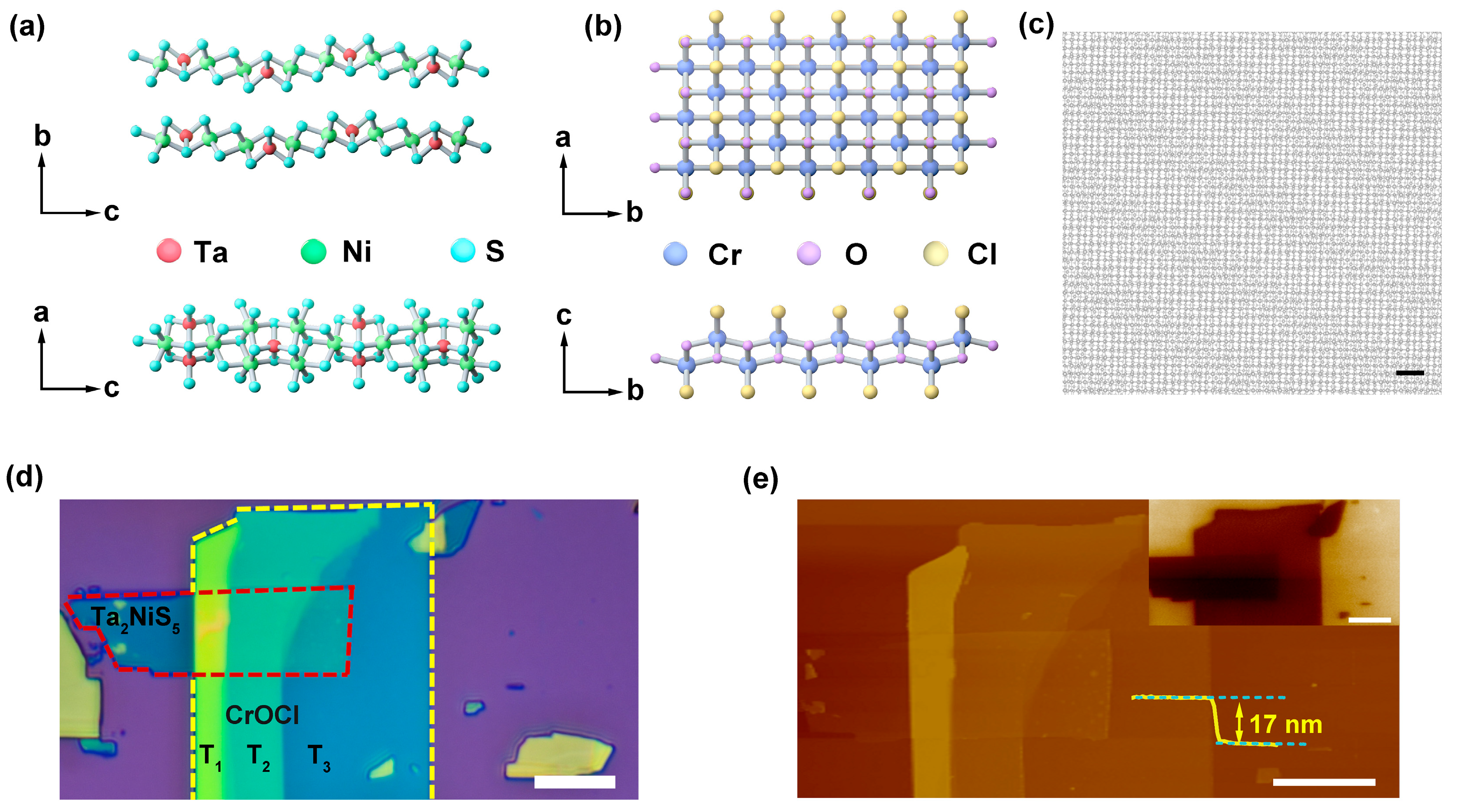
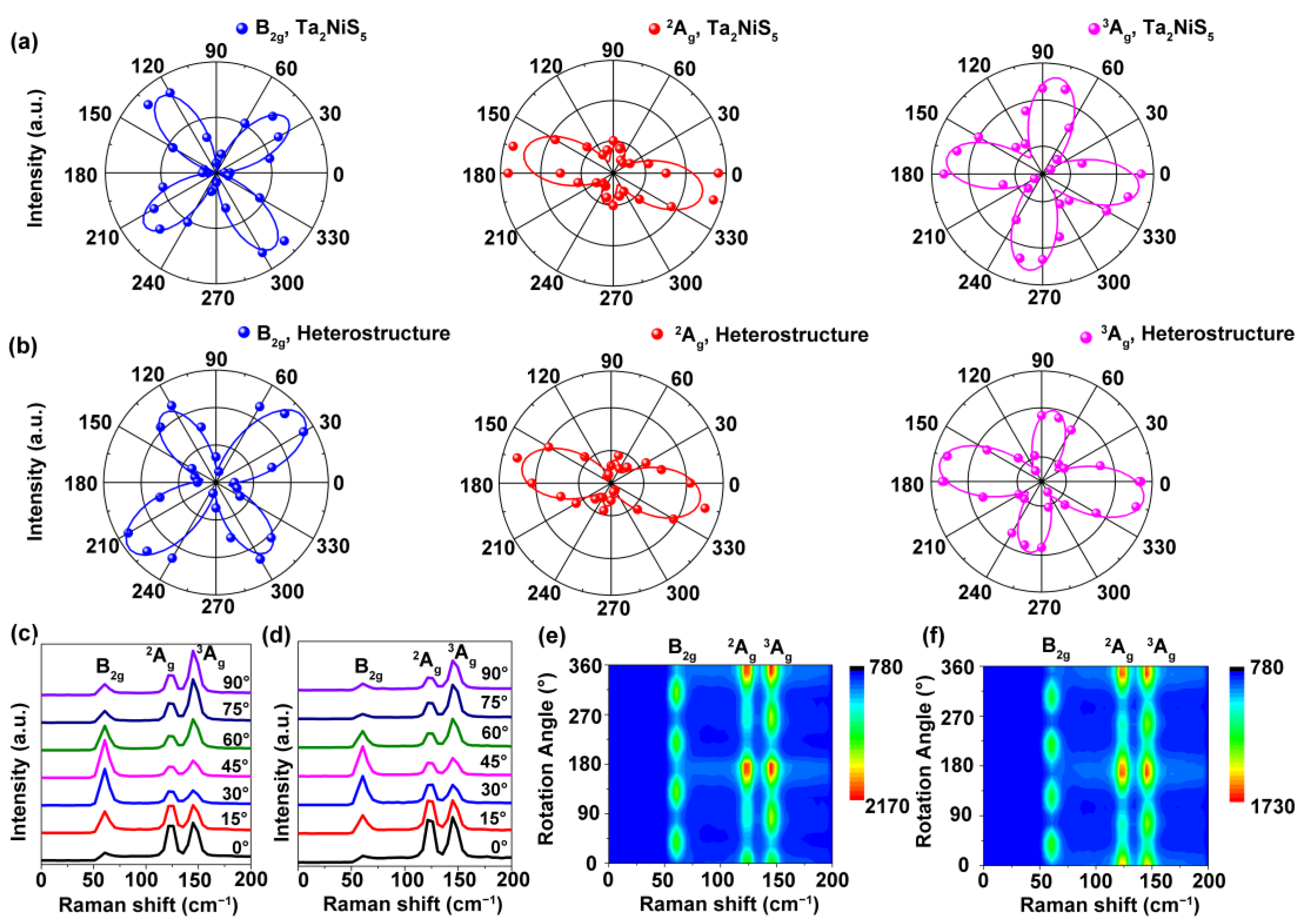
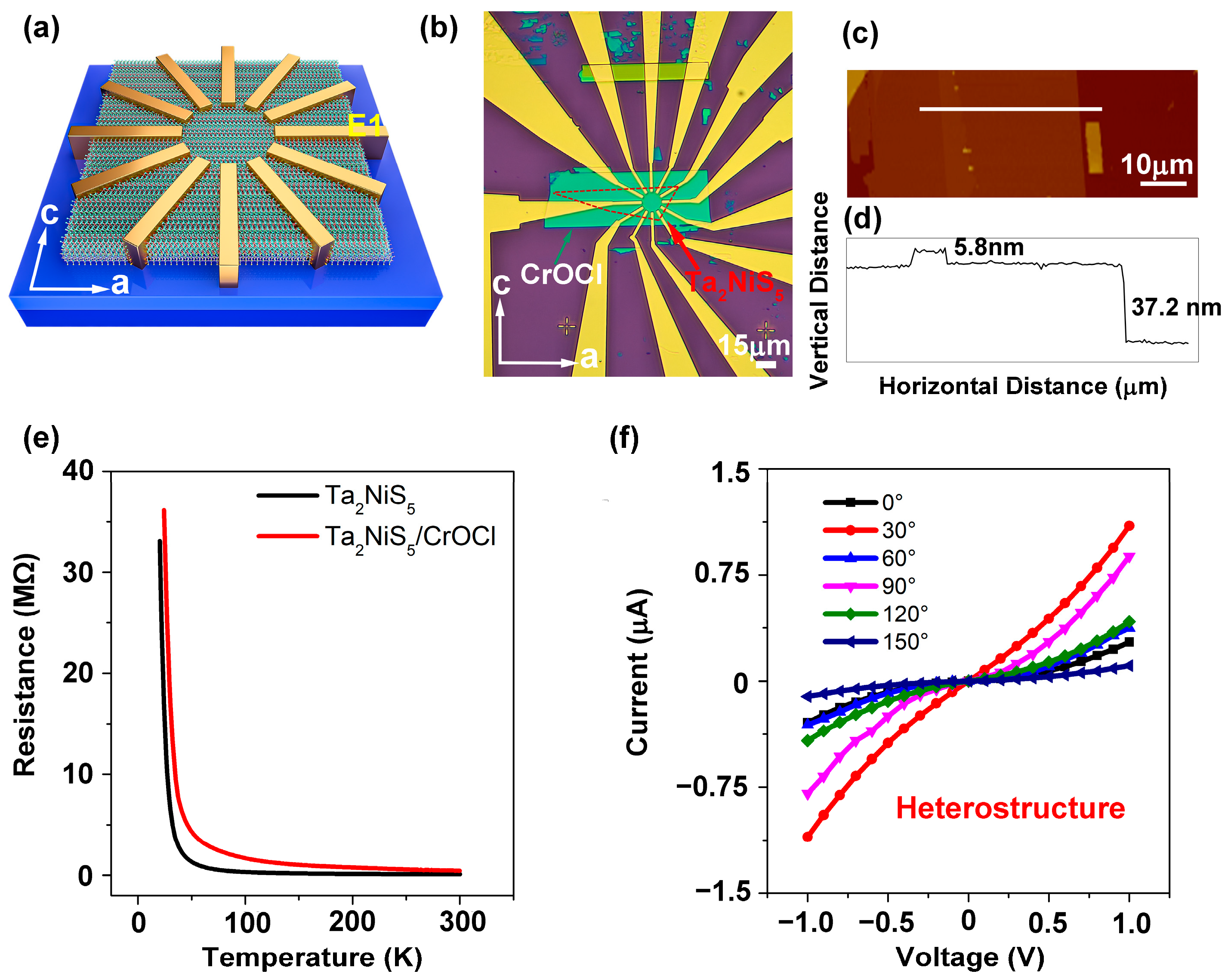
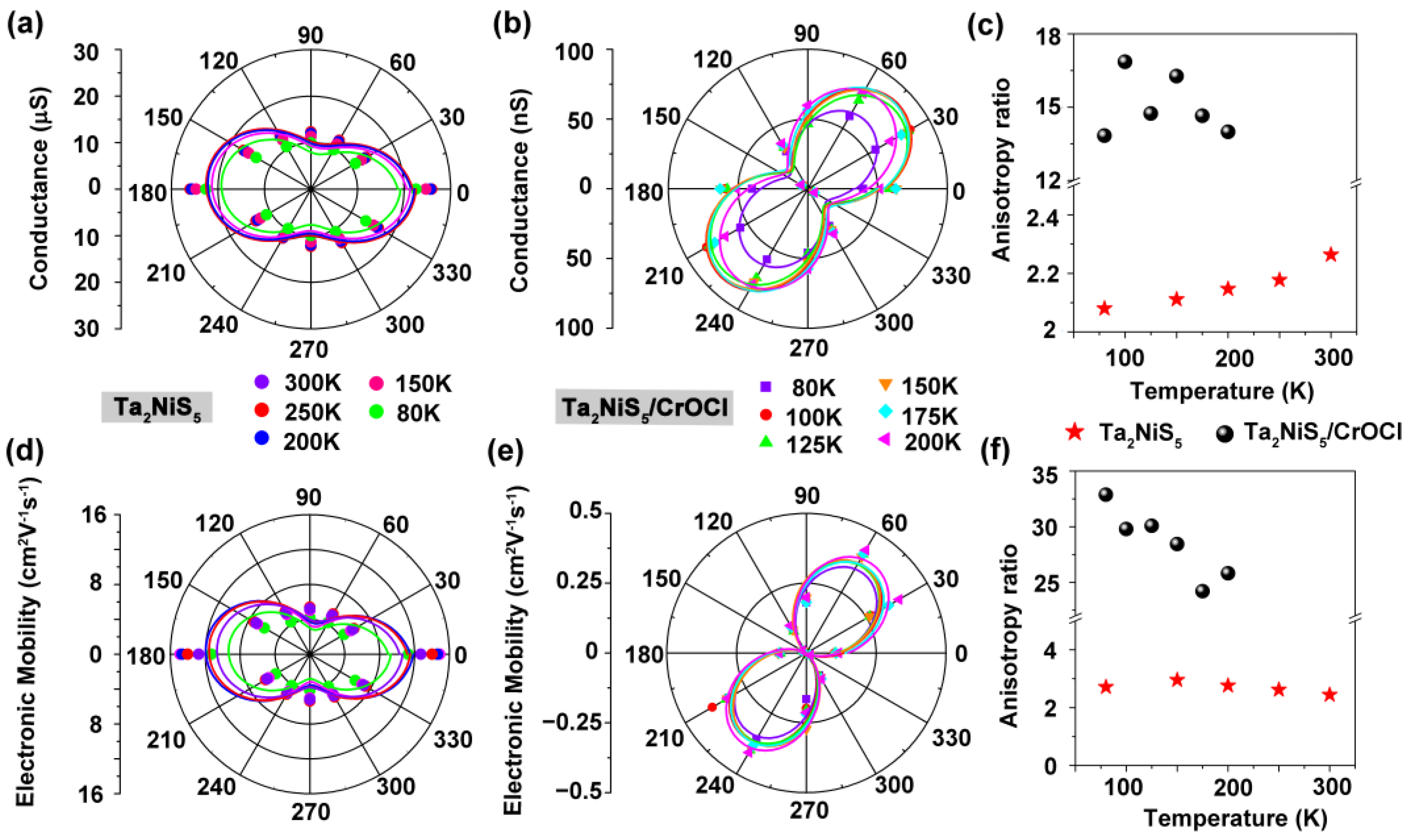
We prepared Ta2NiS5 and CrOCl flakes (Figure S1) from bulk crystals (Onway Technology Co., Ltd., Shanghai, China) via mechanical exfoliation and constructed Ta2NiS5/CrOCl vdW heterostructures using dry transfer via transfer equipment with a 2D location adjustment platform and optical microscope. Due to the anisotropic properties of both Ta2NiS5 and CrOCl, we aligned the a-axis of Ta2NiS5 with the a-axis of CrOCl when constructing the heterostructure. We used polarization Raman spectroscopy to determine the lattice orientation of the material (Figures S2 and S3). Simultaneously, we combined the literature findings to confirm that the long-axis of Ta2NiS5 was the a-axis, while the long-axis of CrOCl was referred to as the a-axis [22,25]. In order to enhance the interlayer coupling of the heterostructure and remove the residual adhesive on the heterostructure surface, we annealed the heterostructure at 325 °C for 1 h. Six pairs of electrodes with Cr/Au (10/70 nm) were fabricated using electron-beam lithography (Raith, Pittsburgh, Germany) and PVD75 e-beam evaporation (Kurt J. Lesker, Pittsburgh, Jefferson Hills, UT, USA). For the Raman spectroscopy (WITEC, Ulm, Germany), we employed a 532 nm laser source and a 100× microscope objective. In the parallel configuration, the incident light polarization (ei) was parallel to the scattered light polarization (es), while in the vertical configuration, ei was vertical to es. We defined the direction as 0° when the a-axis of Ta2NiS5 was parallel to the incident light direction. The laser spot size was less than 500 nm. To avoid sample damage, the laser power was adjusted to less than 1 mw. The electrical characterization of the Ta2NiS5 and Ta2NiS5/CrOCl heterostructures was carried out with a probe station (Lake Shore, Westerville, OH, USA) equipped with a semiconductor analyzer system (Keithley, Cleveland, OH, USA).

3. Results

We chose a ternary transition-metal chalcogenide, Ta2NiS5, and an insulator, CrOCl, as the building blocks of the interface because the compounds have similar rotational and mirror symmetries. The Ta2NiS5 and CrOCl crystal structures are illustrated in Figure 1a,b, both belonging to an orthorhombic structure [23]. When Ta2NiS5 and CrOCl are stacked to form a heterostructure, stripe moiré patterns occur at the Ta2NiS5/CrOCl interface (Figure 1c). The generation of moiré patterns further alters the electrical and optical properties of the heterostructure [26]. Unlike the moiré patterns in twisted graphene, the stripe moiré patterns originate from the lattice mismatch at the Ta2NiS5/CrOCl interface, and it may induce in-plane polarization at this interface via strain [27,28]. In a MoS2/CrOCl heterostructure, this stripe moiré pattern is ascribed to the lattice mismatch between MoS2 and CrOCl, resulting in the strain in the MoS2 [9,12].
Figure 1d shows the optical image of the Ta2NiS5/CrOCl heterostructure. The red-marked region indicates Ta2NiS5, and the yellow-marked region represents multiple thicknesses of CrOCl. Figure 1e corresponds to the atomic force microscope (AFM) image, which provides a higher-resolution view. It can be observed that the surface of the heterostructure is smooth. No crack or fold exists in the overlapping area, indicating the high quality of the interface. The inset is the Kelvin probe force microscopy (KPFM) image of the Ta2NiS5/CrOCl heterostructure. The KPFM image exhibits a highly uniform potential distribution in the overlapping regions, and a significant potential discrepancy can be seen.
We employed angular-resolved polarized Raman spectroscopy to investigate the symmetry of the Ta2NiS5 and Ta2NiS5/CrOCl heterostructures, aiming to uncover the influence of symmetry engineering on the in-plane polarization intensity. For Ta2NiS5, it has a B2g and three Ag vibration modes. The force vectors correspond to a twisting motion for the B2g mode and stretching motions for the 2Ag and 3Ag modes [13]. The polarization plots of each Raman mode are shown in Figure 2a,b. The B2g, 2Ag, and 3Ag modes of pristine Ta2NiS5 and the Ta2NiS5/CrOCl heterostructure exhibit four-lobed shapes. Under the parallel polarization configuration, the B2g mode intensity of pristine Ta2NiS5 had a 90° variation period, while its intensities achieved the maxima at α ≈ 40°, 130°, 220°, and 310°. The B2g mode intensities achieved the maxima in the Ta2NiS5/CrOCl heterostructure at α ≈ 40° and 220° with the sub-maxima at α ≈ 30° and 310°. The anisotropy ratio of B2g intensity increased from 4.6 (Ta2NiS5) to 9 (Ta2NiS5/CrOCl). Similar behavior was observed in the 3Ag mode, where the maximum intensities occurred at α ≈ 170°, and 350° for both pristine Ta2NiS5 and the heterostructure, with sub-maxima at α ≈ 80°, and 260° in the heterostructure. The anisotropy ratio of the 3Ag intensities increased from 2 (Ta2NiS5) to 3.3 (Ta2NiS5/CrOCl). Meanwhile, the 2Ag mode reached its maximum intensities at α ≈ 165° and 345° in both pristine Ta2NiS5 and the Ta2NiS5/CrOCl heterostructure, with sub-maxima at α ≈ 45° and 135°. The anisotropy ratio increased from 3.8 (Ta2NiS5) to 5.9 (Ta2NiS5/CrOCl). By comparing the Raman spectroscopy results of Ta2NiS5 and the Ta2NiS5/CrOCl heterostructure, it can be clearly observed that the asymmetry of Ta2NiS5 was enhanced by constructing the heterostructure.
As shown in Figure 2c, the B2g, 2Ag, and 3Ag of pristine Ta2NiS5 along the a-axis are located at 61.6, 123.7, and 146.1 cm−1. The Raman frequencies of Ta2NiS5 and Ta2NiS5/CrOCl along the a- and c-axes are exhibited in Figure 2d and Table S1, wherein all the Raman frequencies of the heterostructure shift along both the a-axis and c-axis compared with those of the Ta2NiS5. Figure 2e,f shows the contour maps of the Raman intensity varying with the angle for Ta2NiS5 and the heterostructure, respectively. By comparing the Raman spectra of Ta2NiS5 and Ta2NiS5/CrOCl, it can be observed that the Raman frequency shift occurred in the heterostructure. The Raman frequency is influenced by temperature, doping, material thickness, and strain [18,29,30,31]. In our comparative experiments, the same Ta2NiS5 thickness and test temperature were used, and CrOCl was used as an insulator, eliminating the influence of doping. Therefore, we suspect that the Raman shift was mainly caused by strain. When Ta2NiS5 and CrOCl form a vdW heterostructure, the mismatch of their lattice constants leads to lattice reconstruction, reducing the symmetry of Ta2NiS5 and enhancing the polarization. Meanwhile, the lattice mismatch may also cause strain within Ta2NiS5, further affecting the symmetry of the observed Raman modes in it. The B2g, 2Ag, and 3Ag modes represent the distortion and stretching movements of the Raman force vector. When Ta2NiS5 is strained, the Raman frequencies and symmetries of these modes change accordingly, consistent with the experimental phenomena we observed.
In order to further compare the enhancement effect of anisotropy on Ta2NiS5, we characterized the Ta2NiS5/CrOCl heterostructure via angle-dependent electrical transport measurements. Figure 3a shows a schematic diagram of the Ta2NiS5/CrOCl device, where we define 0° as the angle when the electrode E1 is parallel to the a-axis of Ta2NiS5. The side view of the device structure is shown in Figure S4. The electrode was deposited on Ta2NiS5. The channel length was 15 μm, and the angle between adjacent electrodes was 30°. Figure 3b,d displays the optical microscope image, AFM image, and height map image of the Ta2NiS5/CrOCl device. The prepared heterostructure exhibits uniform quality distribution, free of wrinkles and residue, showcasing a high-quality vdW interface. The thicknesses of Ta2NiS5 and CrOCl were 5.8 nm and 37.2 nm, respectively. The I-V curves were measured between distinct diagonal contacts at various temperatures. We tested the temperature-dependent resistance curves of Ta2NiS5 and the Ta2NiS5/CrOCl heterostructure along the a-axis (Figure 3e). With the increase in temperature, the resistance of the a-axis decreased, showing typical semiconductor characteristics, which were similar to those of the pristine Ta2NiS5. Figure 3f presents the Ids–Vds curves of the Ta2NiS5/CrOCl heterostructure at different angles at room temperature. The currents at different angles show significant anisotropy.
To further describe the electrical anisotropy of the heterostructure, we characterized the conductivity and mobility of the Ta2NiS5 and Ta2NiS5/CrOCl devices. At a certain angle θ, the conductivity of anisotropic materials can be expressed as [32]:
σ θ = σ a s i n 2 θ + σ c c o s 2 θ
where σθ represents the conductivity of the sample in the θ direction, σa and σc denote the conductivity along the a- and c-axes, respectively. We measured the electrical conductivity at 80–300 K, as shown in Figure 4a and Table S2. The pristine Ta2NiS5 exhibited mirror symmetry, so its electrical transport properties exhibited two-fold rotational symmetry along the a-axis and c-axis [13]. The electrical conductivity reached its maximum along the a-axis and achieved its minimum along the c-axis. The anisotropy ratio of pristine Ta2NiS5 was approximately 2.1 (Figure 4c), which is similar to the reported value of 1.78–1.41 (80–300 K) in the literature [13]. Figure 4b displays a polar plot of the electrical conductivity of Ta2NiS5/CrOCl at 80–200 K, indicating clear anisotropy in conductance. The angle-dependent conductance exhibits typical two-fold symmetry. The σmax occur at θ = 52° and 232°, while the σmin are present at θ = 142° and 322°. The deviation of the polar axis might be attributed to lattice mismatch at the interface of the heterostructure, leading to a change in the periodic symmetry of the lattice. Similar phenomena have also been observed in other heterostructures [8,33]. Figure 4c shows the comparison of the anisotropy ratio (σmaxmin) of the electrical conductivity of Ta2NiS5 and Ta2NiS5/CrOCl at different temperatures. The anisotropic ratio is approximately 15, which is one order higher than that of the pristine Ta2NiS5 (~2.1).
The corresponding angle-resolved transfer characteristics for Ta2NiS5/CrOCl are shown in Figure S5. The transfer curves at different temperatures and angles demonstrate considerable discrepancies. The anisotropic carrier mobility of Ta2NiS5/CrOCl was estimated according to the equation [34]:
μ = d I d s d V g L W C i V d s
where L and W represent the length and width of the channel. Ci = ε0εr/d is the gate capacitance, ε0 is the vacuum dielectric constant, εr is the relative dielectric constant of SiO2 (for Ta2NiS5) and CrOCl (for Ta2NiS5/CrOCl), and d is the thickness of SiO2 (for Ta2NiS5) and CrOCl (for Ta2NiS5/CrOCl). dIds/dVg represents the maximum slope of the linear region in the transfer curve. The carrier mobility of pristine Ta2NiS5 exhibits a similar dependence on angles to conductivity (Figure 4d). The anisotropy ratio (a/c-axis) of the mobility is approximately 2.7 (Figure 4f, red). The angle-resolved field-effect carrier mobilities are shown in Figure 4e. The maximum mobility occurs at 53° (233°), whereas the minimum is at 143° (323°), giving an anisotropic mobility ratio (μmaxmin) of approximately 32 at 80 K. The anisotropic ratio of mobility decreases with the increase in temperature. At 200 K, the mobilities anisotropic ratio is approximately 25 (Figure 4f, black). The anisotropic ratio of mobilities in the heterostructure is enhanced by one order of magnitude compared with that of the pristine Ta2NiS5. The experimental results of electrical transport once again demonstrate that via symmetry engineering, we successfully enhanced the in-plane anisotropy in Ta2NiS5.
Based on the above experimental results, we conclude that the in-plane anisotropy enhancement of Ta2NiS5/CrOCl might be attributed to the following reasons. The cause of enhanced anisotropy may be attributed to the reduction in lattice symmetry induced by the vdW interface constructed via symmetry engineering. Recent studies also indicate that constructing a vdW interface can reduce lattice symmetry [35,36]. By utilizing the symmetric engineering of functionalized heterointerfaces with anisotropic vdW dielectric SiP2, in-plane polarization was induced within the isotropic single-layer MoS2, resulting in anisotropic conductivity and photoluminescence [37]. Hangyel et al. studied the in-plane anisotropy of graphene induced by strong interlayer interactions with vdW epitaxially grown on MoO3 layers [38]. The in-plane conductivity anisotropy of graphene is 1.43. By constructing a BP/Bi2Se3 heterostructure, anisotropic optical properties were generated within the isotropic Bi2Se3, with the anisotropic ratio of polarization Raman intensity reaching up to 12 [39]. The stripe moiré patterns simulated at the Ta2NiS5/CrOCl interface also reveal that the lattice mismatch led to a decrease in the symmetry of the heterostructure. Furthermore, all the Raman frequencies shifted in the heterostructure compared with those of pristine Ta2NiS5, and the Raman frequency shift could be related to strain, excluding the effects of temperature, doping, and thickness. We speculate that the anisotropy enhancement of Ta2NiS5 may be caused by the strain induced by lattice mismatch at the vdW interface. It has been confirmed in MoS2/CrOCl heterostructures that lattice mismatch between MoS2 and CrOCl results in uniaxial strain in the MoS2 [12]. In addition, Ni et al. predicted that under smaller in-plane strain, anisotropy can be observed in SnSe/GeSe [40]. Thus, we infer that the enhancement of anisotropy in Ta2NiS5/CrOCl might be attributed to the vdW-interface-induced symmetry reduction and the strain.

4. Conclusions

In conclusion, by constructing vdW heterostructures via symmetric engineering, we demonstrated the enhancement of anisotropy in the Ta2NiS5/CrOCl heterostructure via polarized Raman spectroscopy and electrical transport measurements. Angle-resolved polarized Raman spectroscopy revealed that the polarized intensities of the B2g, 2Ag, and 3Ag modes in the heterostructure were enhanced. The anisotropy ratios for the B2g, 2Ag, and 3Ag modes increase from 4.6, 3.8, and 2 in the pristine Ta2NiS5 to 9, 5.9, and 3.3 in the Ta2NiS5/CrOCl heterostructure, respectively. The angle-dependent electrical transport measurements prove that the anisotropic ratio of conductivity and mobility in the heterostructure increased by one order of magnitude compared with those of the pristine Ta2NiS5. The anisotropy ratio of conductivity was enhanced from ~2.1 (Ta2NiS5) to ~15 (Ta2NiS5/CrOCl), and the anisotropy ratio of mobility was enhanced from ~2.7 (Ta2NiS5) to ~32 (Ta2NiS5/CrOCl). The reason for this anisotropic enhancement may have contributed to the lattice mismatch and strain. This study provides inspiration to study symmetry-related van der Waals heterostructures and pave the way to novel nano-electronic devices.

Supplementary Materials

The following supporting information can be downloaded at https://www.mdpi.com/article/10.3390/nano13233050/s1. Figure S1: Photograph of Ta2NiS5 and CrOCl; Figure S2: The angle-dependent Raman spectra of CrOCl flake in parallel configuration; Figure S3: The angle-dependent Raman spectra of CrOCl flake in perpendicular configuration; Figure S4: Schematic diagram of Ta2NiS5/CrOCl device in side view; Figure S5: Transfer characteristic curves of Ta2NiS5/CrOCl device; Table S1: Comparison of Raman frequencies of Ta2NiS5 and Ta2NiS5/CrOCl; Table S2: Comparison of the anisotropy ratios of Ta2NiS5 and Ta2NiS5/CrOCl heterostructure.

Author Contributions

Conceptualization, Y.S. and C.D.; investigation, Y.S. and P.C.; methodology, Y.S.; software, X.X.; formal analysis, Y.S. and C.D.; resources, G.P., X.Z. and C.D.; data curation, Y.S.; writing—original draft preparation, Y.S.; writing—review and editing, C.D., Y.Z. and X.Z.; supervision, C.D. and X.Z.; project administration, G.P. and W.C. All authors have read and agreed to the published version of the manuscript.

Funding

This research was funded by the National Natural Science Foundation of China (NSFC) (grant nos. 11874423 and 11404399).

Data Availability Statement

The data presented in this study are available upon request from the corresponding authors.

Acknowledgments

The authors thank Xiao Guo from the Institute of Physics, the Chinese Academy of Sciences, for his guidance on the discussion of the data and revising of the manuscript.

Conflicts of Interest

The authors declare no conflict of interest. All authors have read and agreed to the published version of the manuscript.

References

  1. Zhong, M.; Meng, H.; Liu, S.; Yang, H.; Shen, W.; Hu, C.; Yang, J.; Ren, Z.; Li, B.; Liu, Y.; et al. In-Plane Optical and Electrical Anisotropy of 2D Black Arsenic. ACS Nano 2021, 15, 1701–1709. [Google Scholar] [CrossRef] [PubMed]
  2. Yan, Y.; Xiong, W.; Li, S.; Zhao, K.; Wang, X.; Su, J.; Song, X.; Li, X.; Zhang, S.; Yang, H.; et al. Direct Wide Bandgap 2D GeSe2 Monolayer toward Anisotropic UV Photodetection. Adv. Opt. Mater. 2019, 7, 1900622. [Google Scholar] [CrossRef]
  3. Xia, F.; Wang, H.; Jia, Y. Rediscovering black phosphorus as an anisotropic layered material for optoelectronics and electronics. Nat. Commun. 2014, 5, 4458. [Google Scholar] [CrossRef] [PubMed]
  4. Yang, S.; Yang, Y.; Wu, M.; Hu, C.; Shen, W.; Gong, Y.; Huang, L.; Jiang, C.; Zhang, Y.; Ajayan, P.M. Highly In-Plane Optical and Electrical Anisotropy of 2D Germanium Arsenide. Adv. Funct. Mater. 2018, 28, 1707379. [Google Scholar] [CrossRef]
  5. Qiu, M.; Sun, Z.T.; Sang, D.K.; Han, X.G.; Zhang, H.; Niu, C.M. Current progress in black phosphorus materials and their applications in electrochemical energy storage. Nanoscale 2017, 9, 13384–13403. [Google Scholar] [CrossRef]
  6. Islam, A.; van den Akker, A.; Feng, P.X.L. Anisotropic Thermal Conductivity of Suspended Black Phosphorus Probed by Opto-Thermomechanical Resonance Spectromicroscopy. Nano Lett. 2018, 18, 7683–7691. [Google Scholar] [CrossRef]
  7. Liu, H.W.; Hu, K.; Yan, D.F.; Chen, R.; Zou, Y.Q.; Liu, H.B.; Wang, S.Y. Recent Advances on Black Phosphorus for Energy Storage, Catalysis, and Sensor Applications. Adv. Mater. 2018, 30, 1800295. [Google Scholar] [CrossRef]
  8. Zhu, W.; Wei, X.; Yan, F.; Lv, Q.; Hu, C.; Wang, K. Broadband polarized photodetector based on p-BP/n-ReS2 heterojunction. J. Semicond. 2019, 40, 092001. [Google Scholar] [CrossRef]
  9. Akamatsu, T.; Ideue, T.; Zhou, L.; Dong, Y.; Kitamura, S.; Yoshii, M.; Yang, D.; Onga, M.; Nakagawa, Y.; Watanabe, K.; et al. A van der Waals interface that creates in-plane polarization and a spontaneous photovoltaic effect. Science 2021, 372, 68–72. [Google Scholar] [CrossRef]
  10. Bai, Y.; Zhou, L.; Wang, J.; Wu, W.; McGilly, L.J.; Halbertal, D.; Lo, C.F.B.; Liu, F.; Ardelean, J.; Rivera, P.; et al. Excitons in strain-induced one-dimensional moire potentials at transition metal dichalcogenide heterojunctions. Nat. Mater. 2020, 19, 1068–1073. [Google Scholar] [CrossRef]
  11. Wang, L.; Shih, E.-M.; Ghiotto, A.; Xian, L.; Rhodes, D.A.; Tan, C.; Claassen, M.; Kennes, D.M.; Bai, Y.; Kim, B.; et al. Correlated electronic phases in twisted bilayer transition metal dichalcogenides. Nat. Mater. 2020, 19, 861–866. [Google Scholar] [CrossRef] [PubMed]
  12. Zheng, X.; Wei, Y.; Zhang, X.; Wei, Z.; Luo, W.; Guo, X.; Liu, J.; Peng, G.; Cai, W.; Huang, H.; et al. Symmetry Engineering Induced In-Plane Polarization in MoS2 through Van der Waals Interlayer Coupling. Adv. Funct. Mater. 2022, 28, 2202658. [Google Scholar] [CrossRef]
  13. Li, L.; Gong, P.; Wang, W.; Deng, B.; Pi, L.; Yu, J.; Zhou, X.; Shi, X.; Li, H.; Zhai, T. Strong In-Plane Anisotropies of Optical and Electrical Response in Layered Dimetal Chalcogenide. ACS Nano 2017, 11, 10264–10272. [Google Scholar] [CrossRef]
  14. Su, Y.; Deng, C.; Liu, J.; Zheng, X.; Wei, Y.; Chen, Y.; Yu, W.; Guo, X.; Cai, W.; Peng, G.; et al. Highly in-plane anisotropy of thermal transport in suspended ternary chalcogenide Ta2NiS5. Nano Res. 2022, 15, 6601–6606. [Google Scholar] [CrossRef]
  15. Tan, C.; Yu, P.; Hu, Y.; Chen, J.; Huang, Y.; Cai, Y.; Luo, Z.; Li, B.; Lu, Q.; Wang, L.; et al. High-Yield Exfoliation of Ultrathin Two-Dimensional Ternary Chalcogenide Nanosheets for Highly Sensitive and Selective Fluorescence DNA Sensors. J. Am. Chem. Soc. 2015, 137, 10430–10436. [Google Scholar] [CrossRef]
  16. Duan, Q.; Yang, L.; He, Y.; Chen, L.; Li, J.; Miao, L.; Zhao, C. Layered Ta2NiS5 Q-Switcher for Mid-Infrared Fluoride Fiber Laser. IEEE Photonics J. 2021, 13, 1–4. [Google Scholar] [CrossRef]
  17. Mu, K.; Chen, H.; Li, Y.; Zhang, Y.; Wang, P.; Zhang, B.; Liu, Y.; Zhang, G.; Song, L.; Sun, Z. Electronic structures of layered Ta2NiS5 single crystals revealed by high-resolution angle-resolved photoemission spectroscopy. J. Mater. Chem. C 2018, 6, 3976–3981. [Google Scholar] [CrossRef]
  18. Luo, Z.; Maassen, J.; Deng, Y.; Du, Y.; Garrelts, R.P.; Lundstrom, M.S.; Ye, P.D.; Xu, X. Anisotropic in-plane thermal conductivity observed in few-layer black phosphorus. Nat. Commun. 2015, 6, 8572. [Google Scholar] [CrossRef] [PubMed]
  19. Yin, S.; Zhang, W.; Tan, C.; Chen, L.; Chen, J.; Li, G.; Zhang, H.; Zhang, Y.; Wang, W.; Li, L. Thermal Conductivity of Few-Layer PtS2 and PtSe2 Obtained from Optothermal Raman Spectroscopy. J. Phys. Chem. C 2021, 125, 16129–16135. [Google Scholar] [CrossRef]
  20. Chen, Y.; Peng, B.; Cong, C.; Shang, J.; Wu, L.; Yang, W.; Zhou, J.; Yu, P.; Zhang, H.; Wang, Y.; et al. In-Plane Anisotropic Thermal Conductivity of Few-Layered Transition Metal Dichalcogenide Td-WTe2. Adv. Mater. 2019, 31, e1804979. [Google Scholar] [CrossRef]
  21. Miao, N.; Xu, B.; Zhu, L.; Zhou, J.; Sun, Z. 2D Intrinsic Ferromagnets from van der Waals Antiferromagnets. J. Am. Chem. Soc. 2018, 140, 2417–2420. [Google Scholar] [CrossRef] [PubMed]
  22. Zhang, T.; Wang, Y.; Li, H.; Zhong, F.; Shi, J.; Wu, M.; Sun, Z.; Shen, W.; Wei, B.; Hu, W.; et al. Magnetism and Optical Anisotropy in van der Waals Antiferromagnetic Insulator CrOCl. ACS Nano 2019, 13, 11353–11362. [Google Scholar] [CrossRef] [PubMed]
  23. Qing, X.; Li, H.; Zhong, C.; Zhou, P.; Dong, Z.; Liu, J. Magnetism and spin exchange coupling in strained monolayer CrOCl. Phys. Chem. Chem. Phys. 2020, 22, 17255–17262. [Google Scholar] [CrossRef] [PubMed]
  24. Wei, Z.; Zheng, X.; Wei, Y.; Zhang, X.; Luo, W.; Liu, J.; Peng, G.; Huang, H.; Lv, T.; Zhang, X.; et al. Van der Waals Interlayer Coupling Induces Distinct Linear Dichroism in WSe2 Photodetectors. Adv. Opt. Mater. 2022, 11, 2201962. [Google Scholar] [CrossRef]
  25. Feng, Y.; Chen, R.; He, J.; Qi, L.; Zhang, Y.; Sun, T.; Zhu, X.; Liu, W.; Ma, W.; Shen, W.; et al. Visible to mid-infrared giant in-plane optical anisotropy in ternary van der Waals crystals. Nat. Commun. 2023, 14, 6739. [Google Scholar] [CrossRef]
  26. Tang, K.; Qi, W. Moire-Pattern-Tuned Electronic Structures of van der Waals Heterostructures. Adv. Funct. Mater. 2020, 30, 2002672. [Google Scholar] [CrossRef]
  27. Sunku, S.S.; Ni, G.X.; Jiang, B.Y.; Yoo, H.; Sternbach, A.; McLeod, A.S.; Stauber, T.; Xiong, L.; Taniguchi, T.; Watanabe, K.; et al. Photonic crystals for nano-light in moire graphene superlattices. Science 2018, 362, 1153–1156. [Google Scholar] [CrossRef]
  28. Yoo, H.; Engelke, R.; Carr, S.; Fang, S.; Zhang, K.; Cazeaux, P.; Sung, S.H.; Hovden, R.; Tsen, A.W.; Taniguchi, T.; et al. Atomic and electronic reconstruction at the van der Waals interface in twisted bilayer graphene. Nat. Mater. 2019, 18, 448–453. [Google Scholar] [CrossRef]
  29. Wei, Y.; Wei, Z.; Zheng, X.; Liu, J.; Chen, Y.; Su, Y.; Luo, W.; Peng, G.; Huang, H.; Cai, W.; et al. Stress Effects on Temperature-Dependent In-Plane Raman Modes of Supported Monolayer Graphene Induced by Thermal Annealing. Nanomaterials 2021, 11, 2751. [Google Scholar] [CrossRef]
  30. Yoon, D.; Son, Y.-W.; Cheong, H. Strain-Dependent Splitting of the Double-Resonance Raman Scattering Band in Graphene. Phys. Rev. Lett. 2011, 106, 155502. [Google Scholar] [CrossRef]
  31. Ferrari, A.C.; Basko, D.M. Raman spectroscopy as a versatile tool for studying the properties of graphene. Nat. Nanotechnol. 2013, 8, 235–246. [Google Scholar] [CrossRef] [PubMed]
  32. Qiu, G.; Du, Y.; Charnas, A.; Zhou, H.; Jin, S.; Luo, Z.; Zemlyanov, D.Y.; Xu, X.; Cheng, G.J.; Ye, P.D. Observation of Optical and Electrical In-Plane Anisotropy in High-Mobility Few-Layer ZrTe5. Nano Lett. 2016, 16, 7364–7369. [Google Scholar] [CrossRef] [PubMed]
  33. Gao, X.G.; Chen, G.X.; Li, D.K.; Li, X.K.; Liu, Z.B.; Tian, J.G. Modulation of photothermal anisotropy using black phosphorus/rhenium diselenide heterostructures. Nanoscale 2018, 10, 10844–10849. [Google Scholar] [CrossRef] [PubMed]
  34. Tian, Z.; Guo, C.; Zhao, M.; Li, R.; Xue, J. Two-Dimensional SnS: A Phosphorene Analogue with Strong In-Plane Electronic Anisotropy. ACS Nano 2017, 11, 2219–2226. [Google Scholar] [CrossRef] [PubMed]
  35. Chaudhary, K.; Tamagnone, M.; Rezaee, M.; Bediako, D.K.; Ambrosio, A.; Kim, P.; Capasso, F. Engineering phonon polaritons in van der Waals heterostructures to enhance in-plane optical anisotropy. Sci. Adv. 2019, 5, 7171. [Google Scholar] [CrossRef] [PubMed]
  36. Xiao, M.; Yang, H.; Shen, W.; Hu, C.; Zhao, K.; Gao, Q.; Pan, L.; Liu, L.; Wang, C.; Shen, G.; et al. Symmetry-Reduction Enhanced Polarization-Sensitive Photodetection in Core-Shell SbI3/Sb2O3 van der Waals Heterostructure. Small 2020, 16, e1907172. [Google Scholar] [CrossRef]
  37. Li, Z.; Huang, J.; Zhou, L.; Xu, Z.; Qin, F.; Chen, P.; Sun, X.; Liu, G.; Sui, C.; Qiu, C.; et al. An anisotropic van der Waals dielectric for symmetry engineering in functionalized heterointerfaces. Nat. Commun. 2023, 14, 5568. [Google Scholar] [CrossRef] [PubMed]
  38. Kim, H.; Kim, J.H.; Kim, J.; Park, J.; Park, K.; Baek, J.-H.; Shin, J.-C.; Lee, H.; Son, J.; Ryu, S.; et al. In-plane anisotropy of graphene by strong interlayer interactions with van der Waals epitaxially grown MoO3. Sci. Adv. 2023, 9, eadg6696. [Google Scholar] [CrossRef]
  39. Mao, N.; Zhang, S.; Wu, J.; Tian, H.; Wu, J.; Xu, H.; Peng, H.; Tong, L.; Zhang, J. Investigation of black phosphorus as a nano-optical polarization element by polarized Raman spectroscopy. Nano Res. 2018, 11, 3154–3163. [Google Scholar] [CrossRef]
  40. Ni, H.; Li, M.; Hu, Y.; Mao, C.; Xue, L.; Zeng, H.; Yan, Z.; Wu, Y.; Zheng, C. Two-dimensional SnSe/GeSe van der Waals heterostructure with strain-tunable electronic and optical properties. J. Phys. Chem. Solids 2019, 131, 223–229. [Google Scholar] [CrossRef]
Figure 1. Characterizations of Ta2NiS5/CrOCl heterostructure. Schematic illustrations of the crystal lattice structure for (a) Ta2NiS5 and (b) CrOCl. (c) Stripe moiré pattern simulation diagram of heterointerface. The scale bar is 1 nm. (d) Optical image and (e) AFM of Ta2NiS5/CrOCl heterostructure. The thickness of Ta2NiS5 is 9.2 nm, and the thicknesses of the T1, T2, and T3 of CrOCl are approximately 61, 27.5, and 17 nm. The inset shows the KPFM image of Ta2NiS5/CrOCl heterostructure. The scale bars in (d,e) are both 10 μm.
Nanomaterials 13 03050 g001
Figure 2. Polarized Raman spectra of Ta2NiS5/CrOCl heterostructure under parallel-polarized configuration. The polar plots of (a) Ta2NiS5 and (b) Ta2NiS5/CrOCl heterostructure for B2g, 2Ag, and 3Ag intensities in a rotation period. Raman spectra for different polarized angles of (c) Ta2NiS5 and (d) Ta2NiS5/CrOCl heterostructure. Contour maps of angular-dependent Raman spectra of (e) Ta2NiS5 and (f) Ta2NiS5/CrOCl heterostructure.
Nanomaterials 13 03050 g002
Figure 3. Characterization of Ta2NiS5/CrOCl device. (a) Schematic view of device structure. The (b) optical image and (c) AFM image of Ta2NiS5/CrOCl device. (d) Height map of Ta2NiS5/CrOCl device that scanned along the white area in (c). (e) Temperature-dependent resistance curves of Ta2NiS5 and Ta2NiS5/CrOCl heterostructure along a-axis. (f) Ids–Vds curves of Ta2NiS5/CrOCl heterostructure with different angles at room temperature.
Nanomaterials 13 03050 g003
Figure 4. Electrical anisotropy of Ta2NiS5 and Ta2NiS5/CrOCl devices. Angle-dependent DC conductance of (a) Ta2NiS5 and (b)Ta2NiS5/CrOCl heterostructure at different temperatures. Angle-dependent electron mobility of (d) Ta2NiS5 and (e) Ta2NiS5/CrOCl heterostructure at different temperatures. (c) Conductivity σ and (f) mobility μ ratio of Ta2NiS5 and Ta2NiS5/CrOCl heterostructure at different temperatures.
Nanomaterials 13 03050 g004
Disclaimer/Publisher’s Note: The statements, opinions and data contained in all publications are solely those of the individual author(s) and contributor(s) and not of MDPI and/or the editor(s). MDPI and/or the editor(s) disclaim responsibility for any injury to people or property resulting from any ideas, methods, instructions or products referred to in the content.

