
Doping-Free Phosphorescent and Thermally Activated Delayed Fluorescent Organic Light-Emitting Diodes with an Ultra-Thin Emission Layer

 , and
, and
Abstract
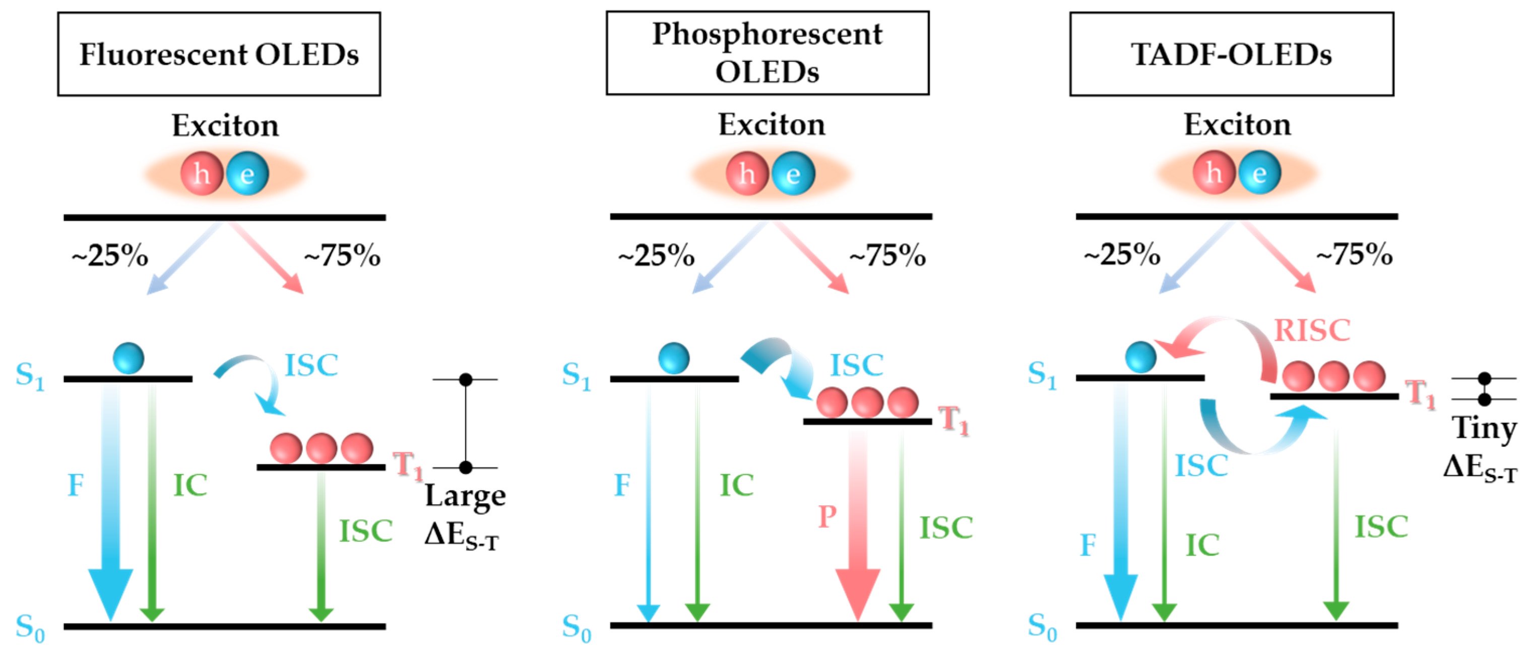
:1. Introduction
2. Materials and Methods
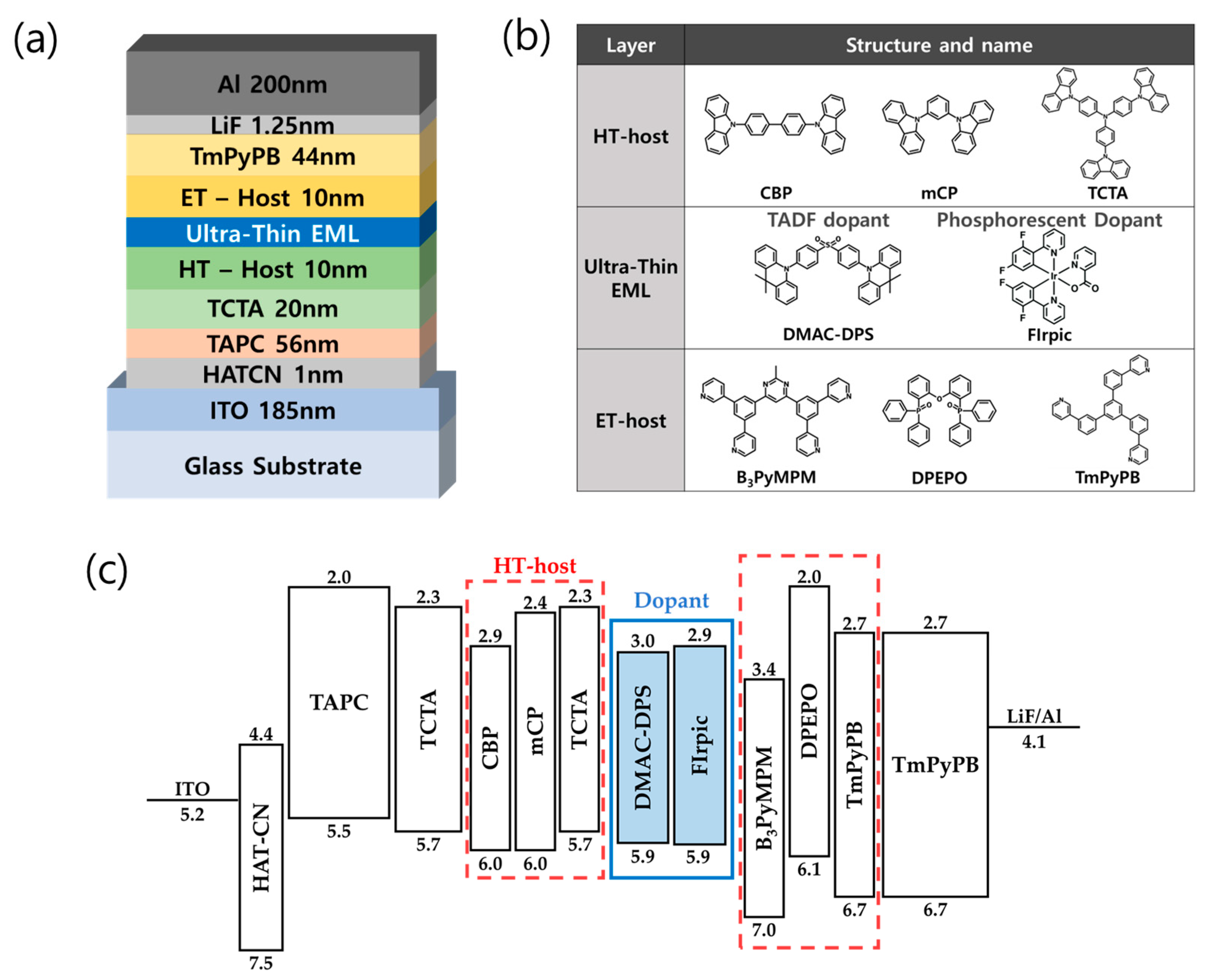
2.1. Device Structure and Characterization
2.2. Experimental Setup and Device Fabrication Methodology
2.3. Characterization and Measurement
3. Results
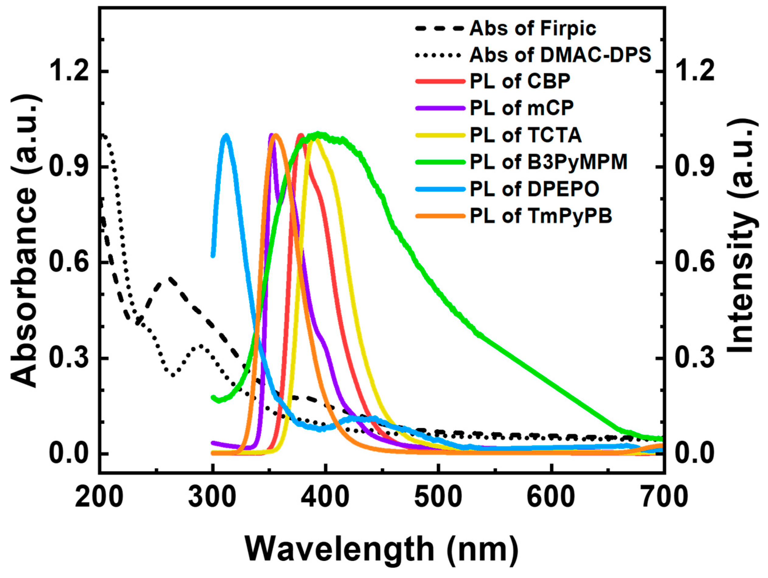
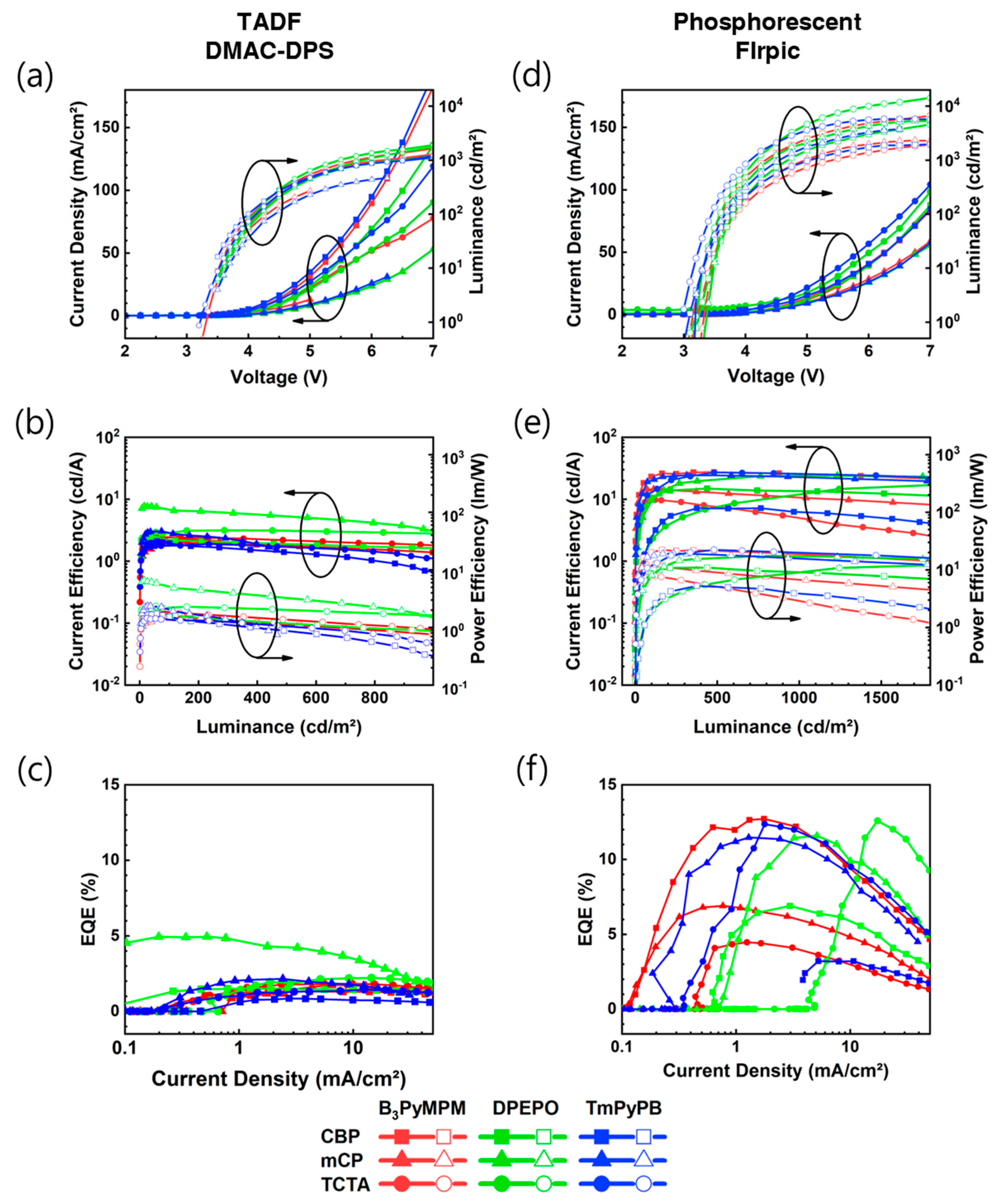
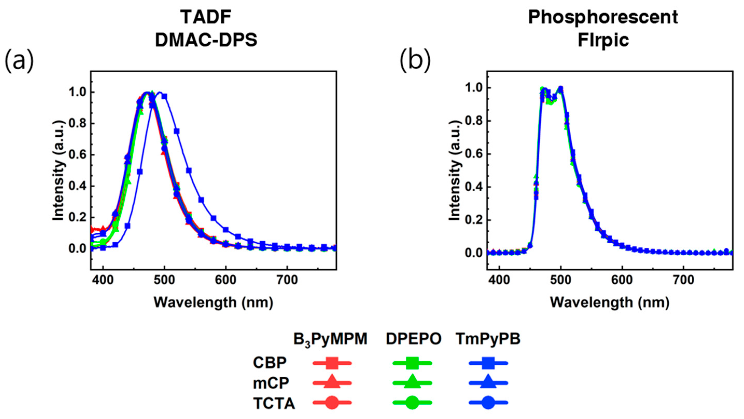
3.1. Analysis of Compatibility between TL Hosts According to Dopant
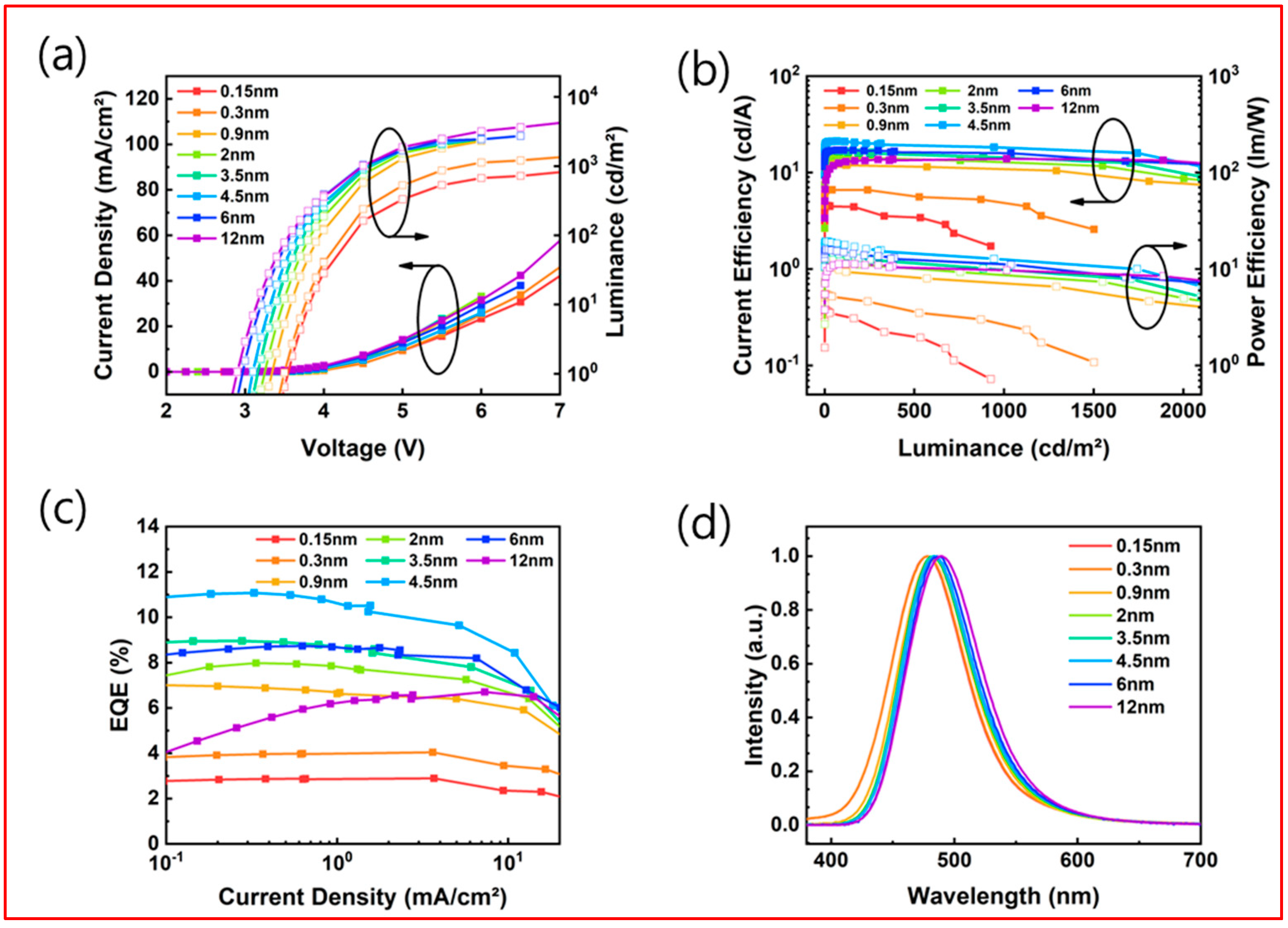
3.2. Analysis of EL Characteristics Depending on DMAC-DPS U-EML Thickness Variation
4. Conclusions
Author Contributions
Funding
Institutional Review Board Statement
Informed Consent Statement
Data Availability Statement
Conflicts of Interest
References
- Tang, C.W.; VanSlyke, S.A. Organic electroluminescent diodes. Appl. Phys. Lett. 1987, 51, 913–915. [Google Scholar] [CrossRef]
- Jou, J.-H.; Kumar, S.; Agrawal, A.; Li, T.-H.; Sahoo, S. Approaches for fabricating high efficiency organic light emitting diodes. J. Mater. Chem. C 2015, 3, 2974–3002. [Google Scholar] [CrossRef]
- Wu, Z.; Ma, D. Recent advances in white organic light-emitting diodes. Mater. Sci. Eng. R Rep. 2016, 107, 1–42. [Google Scholar] [CrossRef]
- Dubey, D.K.; Krucaite, G.; Swayamprabha, S.S.; Yadav, R.A.K.; Blazevicius, D.; Tagare, J.; Chavhan, S.; Hsueh, T.-C.; Vaidyanathan, S.; Grigalevicius, S. Fluorene based amorphous hole transporting materials for solution processed organic light-emitting diodes. Org. Electron. 2020, 79, 105633. [Google Scholar] [CrossRef]
- Xu, R.-P.; Li, Y.-Q.; Tang, J.-X. Recent advances in flexible organic light-emitting diodes. J. Mater. Chem. C 2016, 4, 9116–9142. [Google Scholar] [CrossRef]
- Rogers, J.A.; Someya, T.; Huang, Y. Materials and mechanics for stretchable electronics. Science 2010, 327, 1603–1607. [Google Scholar] [CrossRef]
- Swayamprabha, S.S.; Nagar, M.R.; Yadav, R.A.K.; Gull, S.; Dubey, D.K.; Jou, J.-H. Hole-transporting materials for organic light-emitting diodes: An overview. J. Mater. Chem. C 2019, 7, 7144–7158. [Google Scholar]
- Sekitani, T.; Nakajima, H.; Maeda, H.; Fukushima, T.; Aida, T.; Hata, K.; Someya, T. Stretchable active-matrix organic light-emitting diode display using printable elastic conductors. Nat. Mater. 2009, 8, 494–499. [Google Scholar] [CrossRef]
- Adachi, C.; Baldo, M.A.; Thompson, M.E.; Forrest, S.R. Nearly 100% internal phosphorescence efficiency in an organic light-emitting device. J. Appl. Phys. 2001, 90, 5048–5051. [Google Scholar] [CrossRef]
- Adachi, C. Third-generation organic electroluminescence materials. Jpn. J. Appl. Phys. 2014, 53, 060101. [Google Scholar] [CrossRef]
- Chan, C.-Y.; Tanaka, M.; Lee, Y.-T.; Wong, Y.-W.; Nakanotani, H.; Hatakeyama, T.; Adachi, C. Stable pure-blue hyperfluorescence organic light-emitting diodes with high-efficiency and narrow emission. Nat. Photonics 2021, 15, 203–207. [Google Scholar] [CrossRef]
- Wallwork, N.R.; Mamada, M.; Shukla, A.; McGregor, S.K.; Adachi, C.; Namdas, E.B.; Lo, S.-C. High-performance solution-processed red hyperfluorescent OLEDs based on cibalackrot. J. Mater. Chem. C 2022, 10, 4767–4774. [Google Scholar] [CrossRef]
- Baldo, M.A.; O’Brien, D.F.; You, Y.; Shoustikov, A.; Sibley, S.; Thompson, M.E.; Forrest, S.R. Highly efficient phosphorescent emission from organic electroluminescent devices. Nature 1998, 395, 151–154. [Google Scholar] [CrossRef]
- Singh-Rachford, T.N.; Castellano, F.N. Photon upconversion based on sensitized triplet–triplet annihilation. Coord. Chem. Rev. 2010, 254, 2560–2573. [Google Scholar] [CrossRef]
- Baldo, M.A.; Adachi, C.; Forrest, S.R. Transient analysis of organic electrophosphorescence. II. Transient analysis of triplet-triplet annihilation. Phys. Rev. B 2000, 62, 10967. [Google Scholar] [CrossRef]
- Reineke, S.; Walzer, K.; Leo, K. Triplet-exciton quenching in organic phosphorescent light-emitting diodes with Ir-based emitters. Phys. Rev. B 2007, 75, 125328. [Google Scholar] [CrossRef]
- Murawski, C.; Leo, K.; Gather, M.C. Efficiency roll-off in organic light-emitting diodes. Adv. Mater. 2013, 25, 6801–6827. [Google Scholar] [CrossRef]
- Hu, Y.X.; Miao, J.; Hua, T.; Huang, Z.; Qi, Y.; Zou, Y.; Qiu, Y.; Xia, H.; Liu, H.; Cao, X. Efficient selenium-integrated TADF OLEDs with reduced roll-off. Nat. Photonics 2022, 16, 803–810. [Google Scholar] [CrossRef]
- Zhao, Y.; Chen, J.; Ma, D. Ultrathin nondoped emissive layers for efficient and simple monochrome and white organic light-emitting diodes. ACS Appl. Mater. Interfaces 2013, 5, 965–971. [Google Scholar] [CrossRef]
- Xu, T.; Yang, M.; Liu, J.; Wu, X.; Murtaza, I.; He, G.; Meng, H. Wide color-range tunable and low roll-off fluorescent organic light emitting devices based on double undoped ultrathin emitters. Org. Electron. 2016, 37, 93–99. [Google Scholar] [CrossRef]
- Choi, G.S.; Kang, B.; Choi, J.; Ju, B.-K.; Park, Y.W. Reduced Efficiency Roll-Off in Phosphorescent Organic Light-Emitting Diodes with a Double Dopant. J. Nanosci. Nanotechnol. 2020, 20, 6679–6682. [Google Scholar] [CrossRef]
- Chen, Y.; Chen, J.; Zhao, Y.; Ma, D. High efficiency blue phosphorescent organic light-emitting diode based on blend of hole-and electron-transporting materials as a co-host. Appl. Phys. Lett. 2012, 100, 213301. [Google Scholar] [CrossRef]
- Liu, Z.; Zhang, S.-W.; Zhang, M.; Wu, C.; Li, W.; Wu, Y.; Yang, C.; Kang, F.; Meng, H.; Wei, G. Highly efficient phosphorescent blue-emitting [3+ 2+ 1] coordinated Iridium (III) complex for OLED application. Front. Chem. 2021, 9, 758357. [Google Scholar] [CrossRef] [PubMed]
- Chiba, T.; Pu, Y.-J.; Miyazaki, R.; Nakayama, K.-i.; Sasabe, H.; Kido, J. Ultra-high efficiency by multiple emission from stacked organic light-emitting devices. Org. Electron. 2011, 12, 710–715. [Google Scholar] [CrossRef]
- Nakanotani, H.; Higuchi, T.; Furukawa, T.; Masui, K.; Morimoto, K.; Numata, M.; Tanaka, H.; Sagara, Y.; Yasuda, T.; Adachi, C. High-efficiency organic light-emitting diodes with fluorescent emitters. Nat. Commun. 2014, 5, 4016. [Google Scholar] [CrossRef] [PubMed]
- Strohriegl, P.; Grazulevicius, J.V. Charge-transporting molecular glasses. Adv. Mater. 2002, 14, 1439–1452. [Google Scholar] [CrossRef]
- Kang, J.-W.; Lee, S.-H.; Park, H.-D.; Jeong, W.-I.; Yoo, K.-M.; Park, Y.-S.; Kim, J.-J. Low roll-off of efficiency at high current density in phosphorescent organic light emitting diodes. Appl. Phys. Lett. 2007, 90, 223508. [Google Scholar] [CrossRef]
- Jou, J.-H.; Kumar, S.; Fang, P.-H.; Venkateswararao, A.; Thomas, K.J.; Shyue, J.-J.; Wang, Y.-C.; Li, T.-H.; Yu, H.-H. Highly efficient ultra-deep blue organic light-emitting diodes with a wet-and dry-process feasible cyanofluorene acetylene based emitter. J. Mater. Chem. C 2015, 3, 2182–2194. [Google Scholar] [CrossRef]
- Zhang, X.; Shen, W.; Zhang, D.; Zheng, Y.; He, R.; Li, M. Theoretical investigation of dihydroacridine and diphenylsulphone derivatives as thermally activated delayed fluorescence emitters for organic light-emitting diodes. RSC Adv. 2015, 5, 51586–51591. [Google Scholar] [CrossRef]
- Deng, Z.; Lee, S.; Webb, D.; Chan, Y.; Gambling, W. Carrier transport in thin films of organic electroluminescent materials. Synth. Met. 1999, 107, 107–109. [Google Scholar] [CrossRef]
- Wu, Z.; Liu, Y.; Yu, L.; Zhao, C.; Yang, D.; Qiao, X.; Chen, J.; Yang, C.; Kleemann, H.; Leo, K. Strategic-tuning of radiative excitons for efficient and stable fluorescent white organic light-emitting diodes. Nat. Commun. 2019, 10, 2380. [Google Scholar] [CrossRef] [PubMed]
- Cui, Z.; Ding, J.; Gao, Y.; Li, F. Organic light-emitting diodes based on an Iron (III) complex with doublet emission. CCS Chem. 2022, 4, 2953–2958. [Google Scholar] [CrossRef]
- Zhang, Q.; Li, B.; Huang, S.; Nomura, H.; Tanaka, H.; Adachi, C. Efficient blue organic light-emitting diodes employing thermally activated delayed fluorescence. Nat. Photonics 2014, 8, 326–332. [Google Scholar] [CrossRef]
- Levell, J.; Zhang, S.; Lai, W.-Y.; Lo, S.-C.; Burn, P.; Samuel, I. High power efficiency phosphorescent poly (dendrimer) OLEDs. Opt. Express 2012, 20, A213–A218. [Google Scholar] [CrossRef] [PubMed]
- Kanno, H.; Sun, Y.; Forrest, S.R. High-efficiency top-emissive white-light-emitting organic electrophosphorescent devices. Appl. Phys. Lett. 2005, 86, 263502. [Google Scholar] [CrossRef]
- Kang, S.W.; Baek, D.-H.; Ju, B.-K.; Park, Y.W. Green phosphorescent organic light-emitting diode exhibiting highest external quantum efficiency with ultra-thin undoped emission layer. Sci. Rep. 2021, 11, 8436. [Google Scholar] [CrossRef] [PubMed]
- Kim, H.-B.; Kim, J.-J. Recent progress on exciplex-emitting OLEDs. J. Inf. Disp. 2019, 20, 105–121. [Google Scholar] [CrossRef]
- Tang, F.; Peng, J.; Liu, R.; Yao, C.; Xu, X.; Li, L. A sky-blue fluorescent small molecule for non-doped OLED using solution-processing. RSC Adv. 2015, 5, 71419–71424. [Google Scholar] [CrossRef]
- Lu, M.H.; Sturm, J.C. Optimization of external coupling and light emission in organic light-emitting devices: Modeling and experiment. J. Appl. Phys. 2002, 91, 595–604. [Google Scholar] [CrossRef]
- Zhao, J.; Wang, Z.; Wang, R.; Chi, Z.; Yu, J. Hybrid white organic light-emitting devices consisting of a non-doped thermally activated delayed fluorescent emitter and an ultrathin phosphorescent emitter. J. Lumin. 2017, 184, 287–292. [Google Scholar] [CrossRef]
- Kim, G.H.; Lampande, R.; Im, J.B.; Lee, J.M.; Lee, J.Y.; Kwon, J.H. Controlling the exciton lifetime of blue thermally activated delayed fluorescence emitters using a heteroatom-containing pyridoindole donor moiety. Mater. Horiz. 2017, 4, 619–624. [Google Scholar] [CrossRef]


| Material | LUMO [eV] | HOMO [eV] | Eg 1 [eV] | ET 2 [eV] | μh 3 [cm2 V−1 s−1] | μe 4 [cm2 V−1 s−1] | Function | Reference |
|---|---|---|---|---|---|---|---|---|
| HAT-CN | 4.4 | 7.5 | 3.1 | - | - | - | HIL | [24] |
| TAPC | 2 | 5.5 | 3.5 | 2.87 | 1 × 10⁻³ | 5.0 × 10⁻⁶ | HTL | [25,26] |
| CBP | 2.9 | 6 | 3.1 | 2.6 | 3 × 10⁻⁴ | 1.0 × 10⁻⁸ | HTL | [25,27,28] |
| mCP | 2.4 | 6 | 3.6 | 2.9 | 1.2 × 10⁻⁴ | 5.0 × 10⁻⁶ | HTL | [25,29] |
| TCTA | 2.3 | 5.7 | 3.4 | 2.79 | 3 × 10⁻³ | 1.0 × 10⁻⁸ | HTL | [27,28,30] |
| DMAC-DPS | 2.9 | 5.9 | 3 | 2.91 | - | - | TADF dopant | [31] |
| FIrpic | 3 | 5.9 | 2.9 | 2.65 | - | - | PH dopant | [19] |
| B3PyMPM | 3.4 | 7 | 3.6 | 3.08 | 4.0 × 10⁻³ | HTL | [32,33] | |
| DPEPO | 2 | 6.1 | 4.1 | 3 | 1 × 10⁻⁹ | 5.62 × 10⁻⁶ | HTL | [31] |
| TmPyPB | 2.7 | 6.7 | 4 | 2.75 | 5.0 × 10⁻⁶ | 1.0 × 10⁻³ | HTL | [34] |
| LiF/Al | 4.1 | 4.1 | - | - | - | - | EIL | [35] |
| Emissive Materials: DMAC-DPS | EQE [%] | CE [cd/A] | PE [lm/W] | ||||
|---|---|---|---|---|---|---|---|
| HTL | ETL | Peak | @100 cd/m2 | Peak | @100 cd/m2 | Peak | @100 cd/m2 |
| CBP | B3PyMPM | 1.3 | 1.3 | 2.1 | 2.1 | 1.8 | 1.6 |
| DPEPO | 1.7 | 1.6 | 2.2 | 2.2 | 1.6 | 1.6 | |
| TmPyPB | 1.8 | 1.8 | 2.3 | 2.3 | 1.8 | 1.7 | |
| mCP | B3PyMPM | 1.5 | 1.5 | 2.4 | 2.2 | 2.1 | 1.6 |
| DPEPO | 4.9 | 4.3 | 7.7 | 6.6 | 5.8 | 4.8 | |
| TmPyPB | 2.2 | 1.9 | 3.1 | 2.8 | 2.4 | 2.2 | |
| TCTA | B3PyMPM | 0.9 | 0.8 | 2.0 | 1.9 | 1.7 | 1.5 |
| DPEPO | 2.1 | 2.0 | 3.0 | 2.8 | 2.3 | 1.9 | |
| TmPyPB | 1.5 | 1.3 | 1.9 | 1.8 | 1.5 | 1.4 | |
| Emissive Materials: FIrpic | EQE [%] | CE [cd/A] | PE [lm/W] | ||||
|---|---|---|---|---|---|---|---|
| HTL | ETL | Peak | @100 cd/m2 | Peak | @100 cd/m2 | Peak | @100 cd/m2 |
| CBP | B3PyMPM | 12.7 | 12.2 | 9.0 | 9.4 | 7.9 | 7.8 |
| DPEPO | 6.9 | 4.8 | 14.0 | 14.6 | 12.2 | 12.1 | |
| TmPyPB | 4.5 | 2.1 | 27.3 | 26.2 | 22.1 | 19.4 | |
| mCP | B3PyMPM | 6.9 | 6.2 | 14.8 | 13.4 | 11.0 | 8.9 |
| DPEPO | 11.6 | 11.6 | 24.1 | 24.1 | 16.8 | 16.8 | |
| TmPyPB | 12.6 | 6.9 | 26.7 | 14.6 | 16.8 | 10.8 | |
| TCTA | B3PyMPM | 3.2 | 2.7 | 7.2 | 5.9 | 5.3 | 3.5 |
| DPEPO | 11.5 | 10.9 | 24.3 | 23.0 | 19.1 | 16.1 | |
| TmPyPB | 12.4 | 12.0 | 27.0 | 26.2 | 22.3 | 20.5 | |
| Thickness of U-EML [nm] | Von 1 [V] | EQE [%] | CE [cd/A] | PE [lm/W] | |||
|---|---|---|---|---|---|---|---|
| Peak | @500 cd/m2 | Peak | @500 cd/m2 | Peak | @500 cd/m2 | ||
| 0.15 | 3.6 | 2.9 | 2.3 | 4.5 | 3.4 | 3.8 | 1.9 |
| 0.3 | 3.5 | 4.0 | 3.5 | 6.6 | 5.6 | 5.5 | 3.5 |
| 0.9 | 3.3 | 7.0 | 6.4 | 12.9 | 11.4 | 11.9 | 8.0 |
| 2.0 | 3.3 | 8.2 | 7.3 | 14.8 | 13.3 | 12.7 | 9.3 |
| 3.5 | 3.2 | 9.0 | 7.8 | 16.9 | 14.6 | 15.7 | 10.2 |
| 4.5 | 3.1 | 11.1 | 10.5 | 21.2 | 20.0 | 19.4 | 15.7 |
| 6.0 | 3.0 | 8.7 | 8.6 | 17.0 | 16.7 | 13.1 | 13.1 |
| 12.0 | 2.9 | 6.7 | 6.6 | 13.9 | 13.7 | 11.3 | 10.8 |
Disclaimer/Publisher’s Note: The statements, opinions and data contained in all publications are solely those of the individual author(s) and contributor(s) and not of MDPI and/or the editor(s). MDPI and/or the editor(s) disclaim responsibility for any injury to people or property resulting from any ideas, methods, instructions or products referred to in the content. |
© 2023 by the authors. Licensee MDPI, Basel, Switzerland. This article is an open access article distributed under the terms and conditions of the Creative Commons Attribution (CC BY) license (https://creativecommons.org/licenses/by/4.0/).
Share and Cite
Jang, E.-B.; Choi, G.-S.; Bae, E.-J.; Ju, B.-K.; Park, Y.-W. Doping-Free Phosphorescent and Thermally Activated Delayed Fluorescent Organic Light-Emitting Diodes with an Ultra-Thin Emission Layer. Nanomaterials 2023, 13, 2366. https://doi.org/10.3390/nano13162366
Jang E-B, Choi G-S, Bae E-J, Ju B-K, Park Y-W. Doping-Free Phosphorescent and Thermally Activated Delayed Fluorescent Organic Light-Emitting Diodes with an Ultra-Thin Emission Layer. Nanomaterials. 2023; 13(16):2366. https://doi.org/10.3390/nano13162366
Chicago/Turabian StyleJang, Eun-Bi, Geun-Su Choi, Eun-Jeong Bae, Byeong-Kwon Ju, and Young-Wook Park. 2023. "Doping-Free Phosphorescent and Thermally Activated Delayed Fluorescent Organic Light-Emitting Diodes with an Ultra-Thin Emission Layer" Nanomaterials 13, no. 16: 2366. https://doi.org/10.3390/nano13162366
APA StyleJang, E.-B., Choi, G.-S., Bae, E.-J., Ju, B.-K., & Park, Y.-W. (2023). Doping-Free Phosphorescent and Thermally Activated Delayed Fluorescent Organic Light-Emitting Diodes with an Ultra-Thin Emission Layer. Nanomaterials, 13(16), 2366. https://doi.org/10.3390/nano13162366