Article

Transport Characteristics of Silicon Multi-Quantum-Dot Transistor Analyzed by Means of Experimental Parametrization Based on Single-Hole Tunneling Model

1
Department of Semiconductor Science, Dongguk University-Seoul, Seoul 04620, Republic of Korea
2
Quantum-Functional Semiconductor Research Center, Dongguk University-Seoul, Seoul 04620, Republic of Korea
*
Author to whom correspondence should be addressed.
Nanomaterials 2023, 13(11), 1809; https://doi.org/10.3390/nano13111809
Submission received: 24 April 2023 / Revised: 29 May 2023 / Accepted: 2 June 2023 / Published: 5 June 2023

Abstract

:
The transport characteristics of a gate-all-around Si multiple-quantum-dot (QD) transistor were studied by means of experimental parametrization using theoretical models. The device was fabricated by using the e-beam lithographically patterned Si nanowire channel, in which the ultrasmall QDs were self-created along the Si nanowire due to its volumetric undulation. Owing to the large quantum-level spacings of the self-formed ultrasmall QDs, the device clearly exhibited both Coulomb blockade oscillation (CBO) and negative differential conductance (NDC) characteristics at room temperature. Furthermore, it was also observed that both CBO and NDC could evolve along the extended blockade region within wide gate and drain bias voltage ranges. By analyzing the experimental device parameters using the simple theoretical single-hole-tunneling models, the fabricated QD transistor was confirmed as comprising the double-dot system. Consequently, based on the analytical energy-band diagram, we found that the formation of ultrasmall QDs with imbalanced energetic natures (i.e., imbalanced quantum energy states and their imbalanced capacitive-coupling strengths between the two dots) could lead to effective CBO/NDC evolution in wide bias voltage ranges.

1. Introduction

Recently, to manipulate the vast amount of electronic information data (e.g., big data processes, artificial intelligence, the Internet of Things, etc.), many research groups have devoted their work to demonstrating how novel semiconductor quantum-dot (QD) devices can realize future quantum computations [1,2,3,4,5]. Among various semiconductor QD devices, the silicon (Si) QD-based single-electron (or single-hole) tunnel-junction transistor is one of the most promising device schemes because of its unique transfer and output characteristics. Namely, owing to the strong sub-band modulation in Si QDs, one could effectively demonstrate the unique features of both Coulomb blockade oscillation (CBO) and negative differential conductance (NDC) in a single device system even at room temperature [6,7,8,9,10,11]. Additionally, from both scientific and technical perspectives, the Si process platform is still powerful for driving significant advancements in future nanodevice fabrication technology. By utilizing CBO and NDC characteristics, several types of extraordinary data-processing circuits have been conceived and demonstrated on various Si QD device architectures (e.g., multi-functional logic circuits [12], multi-valued logic circuits [8,13], stochastic data-processing circuits [14,15], quantum cellular automata [16], etc.). To establish a tangible application platform of such astonishing functionalities, the precise control of single-electron (or single-hole) tunneling must be satisfied, particularly at an elevated temperature above 300 K. In other words, electrical one-electron (or one-hole) addition energy (i.e., charging/discharging energy for single-electron (or one-hole) tunneling into/from the Si QD) should be precisely controlled by changing the external bias voltages of the fabricated QD tunnel-junction transistor. Typically, the dot potential of the three-terminal QD transistor is controlled by the gate voltage (VG) and the drain voltage (VD) of the QD transistor so that the CBO and NDC behaviors can take place via one-by-one single-electron (or one-hole) tunneling through the quantum energy states. In lithographically patterned CMOS-compatible Si QD transistors, however, co-tunneling effects and thermally activated carrier conduction often occur because of the parasitic metal-oxide-semiconductor field-effect transistor (MOSFET) [17,18,19]. To solve this issue, in our previous studies we investigated effective ways to reduce thermal quenching and thermal broadening of CBO and NDC by forming an ellipsoidal Si QD structure [8,20] and/or constructing a Si multi-QD system [12,21]. The former utilizes the large quantum-level spacings of the ellipsoidal Si single-QD system, and the latter uses the reduced electron temperature in the multiple-tunnel-junction system. To take full advantage of these Si QD transistors, as a primary task, one needs to understand their transport mechanisms. In the case of single-QD systems, the single-electron (or single-hole) transport mechanisms are well understood due to many substantial studies being conducted on both theoretical models and experimental analyses [22,23,24,25,26,27,28]. However, in the case of the multi-QD devices, experimental understandings of their transport behaviors were somewhat restricted because of stochastic tunneling events. Therefore, it is essential to find an easy approach that can enable experimental understandings of the single-electron (or single-hole) transport mechanisms in the multi-QD transistors.
Based upon all of the above background information, we fabricated a Si multi-QD transistor and characterized its transport mechanisms by means of experimental parametrization, which was fully based on the theoretical single-hole-tunneling model. The device was devised in the form of the gate-all-around (GAA) Si nanowire-channel MOSFET, in which self-assembled multiple Si QDs were created along the Si nanowire channel. Herein, the single-hole transport characteristics of the fabricated Si multi-QD transistor are thoroughly examined and discussed through comprehensive studies on both experimental characterization and theoretical analysis.

2. Experimental Section

Figure 1a schematically illustrates the device configuration of the fabricated Si multi-QD transistor, which was constructed in the form of the CMOS-compatible GAA Si nanowire-channel MOSFET. To devise such an architecture, firstly, the [100] Si nanowire channel (l: 200 nm, w: 40 nm) was patterned by e-beam lithography onto the silicon-on-insulator substrate (tSi: 10 nm). Subsequently, the volumetric size of the patterned Si nanowire was further reduced by isotropic wet etching using the SC-1 solution (NH4OH:H2O2:H2O = 1:1:6). Through this step, the width of the Si nanowire was shrunk to be approximately 10 nm (Figure 1b). Next, with the aim of constructing the GAA structure, a part of the buried oxide (i.e., SiO2 underneath the Si nanowire) was removed through oxide etching by using diluted hydrogen fluoride (HF:H2O = 1:10). After this step, only a small part of the Si nanowire channel was suspended from the buried oxide because the large source (S) and drain (D) areas could still support the beam shape of the Si nanowire channel. To create the gate oxide of the GAA MOSFET structure, the surface of the suspended Si nanowire channel was then oxidized through dry oxidation at 900 °C. Due to oxidation of the Si nanowire surface, the cross-sectional diameter of the Si nanowire (dNW) was eventually further decreased down to approximately 5 nm [6,29]. Thereafter, the formation of the GAA stack was completed by depositing the additional layers of SiO2 (approximately 30 nm) and polycrystalline n+-Si (approximately 250 nm). Finally, the S and D reservoirs (p ≈ 1020 cm−3) were formed by BF2+ ion implantation and thermal activation at 950 °C.

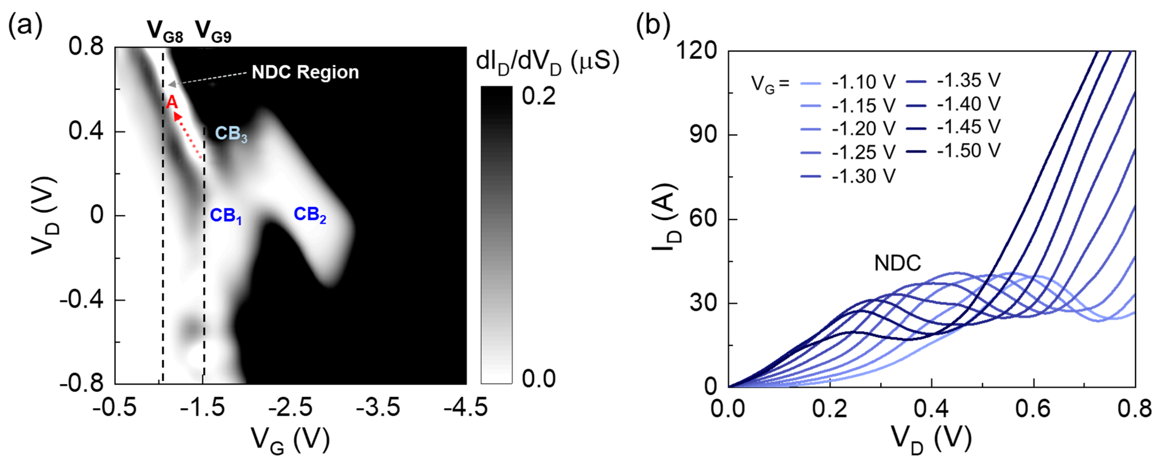
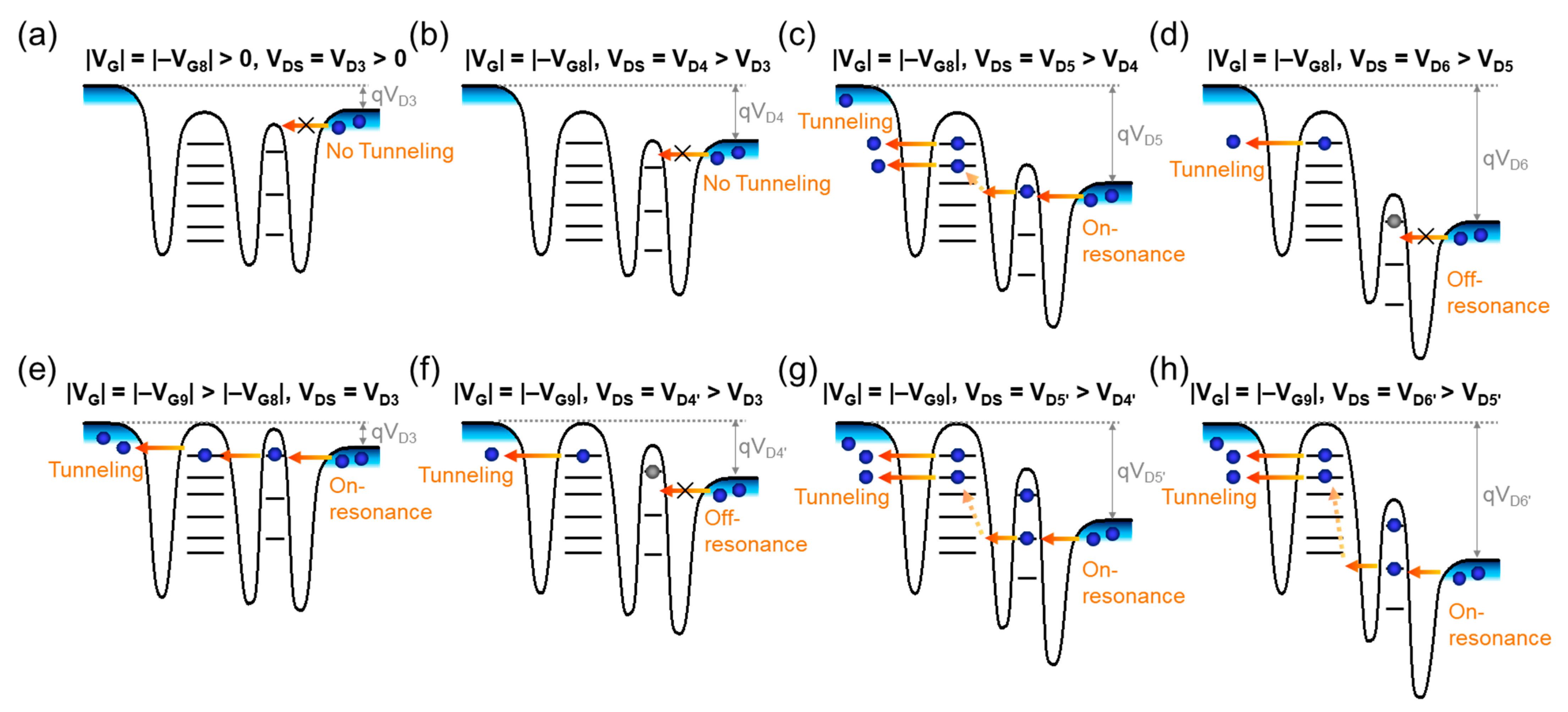
3. Results and Discussion

Prior to discussing the electrical characteristics of the fabricated device, we will explain our device fabrication method that was employed to perform the room-temperature operation of the fabricated Si QD transistor. We obtained the self-created Si QDs through oxidation of the volumetrically undulated ultra-narrow Si nanowire. Notably, no intentional design of the QD sites and sizes was employed in our experiment. According to previous studies [30,31,32,33,34,35], there are two main approaches to devise two types of high-performance Si QD transistors: one is Si QD transistors based on epitaxially grown Si QDs [30,31,32], and the other is lithographically fabricated Si QD transistors [30,31,32]. Although the former could allow for the operation of the fabricated devices at elevated temperatures, the method is inappropriate for practical applications because of difficulties in both size and site controls. On the other hand, the latter is useful for controlling both the size and the site of the QDs. Hence, many researchers have devoted their studies to fabricating high-performance Si QD transistors by using lithography techniques. For example, forming the double/multiple barrier tunnel junctions by pattern-dependent oxidation (PADOX) [36,37,38] and creating the electrical dots/barriers by side-gate formation [39,40,41] are typical examples that can enable the fabrication of high-performance CMOS-compatible Si QD transistors. When considering the device operation temperature, however, these techniques do not satisfy the conditions for room-temperature operation because conventional lithography techniques only allow for the formation of large QD sizes and small tunnel barrier heights. We therefore adopted the QD self-formation method by using a volumetrically undulated ultra-narrow Si nanowire. Although the proposed method cannot ensure the precise size/site/number control of the Si QDs, we believe the method will be good for use in future CMOS-compatible Si QD device technology. This is because the method used here is already compatible with CMOS fabrication processes and can be further developed when advanced nanolithography techniques are well established in the near future. In other words, if the intentional patterning of the regularly undulated sub-5 nm Si nanowire is available when using the advanced lithography techniques (e.g., extreme ultraviolet lithography [42,43], heavy-ion lithography [44], scanning probe lithography [45], block copolymer self-assembly [46], etc.), one can easily control the number, sizes, and sites of the Si QDs by employing the PADOX process method as well.
Next, we interpreted the QD nature inside the volumetrically undulated ultra-narrow Si nanowire channel. As schematically illustrated in Figure 1c, during the isotropic wet-etching process, the magnitude of dNW fluctuated along the undulated Si nanowire direction. Here, it can be noticed that such a volumetric dNW fluctuation is much more significant after thermal oxidation of the Si nanowire surface. Thus, the dNW sizes at the squeezed regions are much smaller than 5 nm because the dNW at the central Si nanowire area was confirmed to be approximately 5 nm [6,29]. According to the quantum-mechanical energy-band calculation [47,48,49], the sub-band modulation in the [100] Si nanowire significantly increases with decreasing dNW. For instance, when dNW is <2 nm in the [100] Si nanowire, the ground state is located at more than 400 meV below the valence band (EV) of the bulk Si [8,48]. In the present type of the volumetrically undulated Si nanowire channel, therefore, the Si multi-QD system can be self-assembled along the nanowire. In other words, the large potential barriers are formed at the squeezed Si nanowire areas (i.e., dNW << 5 nm), and the quantum dots are created at the rest areas (i.e., dNW ≈ 5 nm), as represented in Figure 1d. This allows the fabricated GAA Si nanowire-channel MOSFET to act as the Si multi-QD transistor. At this point, one can disregard the presence of large dots since their quantum-level spacings are too small to significantly contribute to the tunneling transport characteristics. In short, at 300 K, both the large thermal fluctuation at the bigger dots and the broad hole carrier distribution at the S/D reservoirs smear the presence of the large dots. Additionally, it should be remembered that the GAA gate stacks cover the nanowire edges at the S/D and multi-QD regions. Thus, these two nanowire edges (i.e., extended S/D regions) play a role as the parasitic MOSFET (Figure 1e), which may eventually give rise to the increase in the valley current of the present CMOS-compatible GAA MOSFET-based Si multi-QD transistor. For example, when the gate bias voltage (VG) is greater than the threshold voltage (Vth) of the parasitic MOSFET, the drift current component of the parasitic MOSFET largely contributes to the increase in total drain current (ID) of the actual device (Figure 2a). This would, in turn, smear out the CBO features at the higher VG region.
Despite such a parasitic MOSFET effect, the fabricated Si multi-QD transistor clearly exhibits two large CBO peaks at 300 K in its ID–VG characteristic curves (Figure 2b). The magnitudes of the peak-to-valley current ratio (PVCR) are 261 and 288 for the first CBO1 and the second CBO2, respectively. In addition, the values of the full width at half-maximum (FWHM) are approximately 192 and 188 mV for CBO1 and CBO2, respectively. In principle, for the room-temperature observation of such clear CBO characteristics, the one-electron (or hole)-addition energy (Ea) should be sufficiently larger than the thermal energy at room temperature (i.e., Eth ≈ 26 meV at 300 K) [20,50]. Ea is given by
E a = E C + Δ ε
E C = q 2 / C Q D
C Q D = 2 π ε ε 0 d Q D
where EC, Δε, q, CQD, ε, ε0, and dQD are the charging energy, quantum-level spacing, unit charge, QD capacitance, dielectric constant of SiO2, and vacuum permittivity, respectively. Thus, one can conclude that the present device includes ultrasmall QDs (i.e., dQD < 5 nm) inside the Si nanowire channel. Furthermore, since both PVCR and FWHM are closely related to the thermal fluctuation of the QDs [51,52], the observed large PVCR and small FWHM values obviously indicate that the present device contains ultrasmall QDs that may possess large Δε values (>>26 meV).
The existence of the ultrasmall QDs can be further elucidated from the charge stability diagram of the fabricated Si multi-QD transistor. As denoted by CB1 and CB2 in Figure 3a, the device exhibits the two Coulomb blockade regions, which correspond to CBO1 and CBO2 in Figure 2b, respectively. Here, it should be noticed that both the CB1 and CB2 regions are extended toward the A and B directions. In the case of CB1, particularly, the extended CB regions do not disappear even at a high VD up to ±0.8 V. According to our previous studies [51,53], such a long and clear CB extension is attributed to both the large quantum-level spacings and the large tunneling barrier heights. Additionally, as indicated by CB3, the present device shows the overlapped CB region, which is also extended toward the A’ and B’ directions. This depicts how present device comprises the multi-QD system with irregular dot-and-barrier shapes. As previously mentioned, in the present device, the multi-QD system was self-formed along the undulated Si nanowire at the volumetrically shrunken areas (i.e., squeezed regions = tunnel barriers and their adjacent areas = dots). Thus, both the quantum-level spacings and the tunnel barrier heights are inhomogeneous. This might result in imbalanced energetic CB conditions for each QD; hence, the stochastic tunneling events would occur throughout the entire multi-QD system [54]. Therefore, some parts of the adjacent CB regions could be overlapped at certain bias voltages.
The split of the CBO peaks can also verify the formation of the multi-QD system. For example, when applying a high VD that can break a certain stochastic tunneling condition, the multi-QD system begins to renormalize its energetic condition for stochastic tunneling. Namely, some of the quantum states start and/or stop contributing their energetic pathways to the renormalized stochastic tunneling transport condition. Then, the CBO peaks eventually split at the high VD [12]. In the present device, as can be seen from Figure 3b, the CBO peaks are split at the high VD region so that the additional CB3 region starts appearing in between the CB1 and CB2 regions. This corresponds to the extension of the CB3 region toward the A’ direction, as observed in the charge stability diagram (Figure 3a). Based upon these results, one can surmise that the present device is composed of multiple Si QDs. According to both theoretical and experimental studies [21,55], the formation of the multi-QD system is helpful for reducing the co-tunneling effect so that the valley current (Ivalley) of the CBO can be decreased at the higher VD region. Correspondingly, the present device exhibits the clear valley states even at a high VD above 0.5 V (Figure 3b).
According to the co-tunneling model [21,56], Ivalley is given by
I valley G b N + 1 { ( e V D ) 2 + ( 2 π k B T e f f ) 2 } N V D
where G b N + 1 is the conductance multiplication for every tunnel barrier, N is the number of QDs, kB is the Boltzmann constant, and Teff is the effective electron temperature. Therefore, one can easily deduce the number of QDs by using the above equation. For example, when N = 1 (i.e., single-QD system), 2 (i.e., double-QD system), and 3 (i.e., triple-QD system), Ivalley can be described as follows:
I valley ( N = 1 ) = α G S G D { e 2 V D 3 + ( 2 π k B T e f f ) 2 V D }
I valley ( N = 2 ) = β G S G i G D { e 4 V D 5 + 2 e 2 ( 2 π k B T e f f ) 2 V D 3 + ( 2 π k B T e f f ) 4 V D }
I valley ( N = 3 ) = γ G S G i 1 G i 2 G D { e 6 V D 7 + 3 e 4 ( 2 π k B T e f f ) 2 V D 5 + 3 e 2 ( 2 π k B T e f f ) 4 V D 3 + ( 2 π k B T e f f ) 6 V D }
where α, β, and γ are the proportional factors, and GS, Gi, and GD are the source, intermediate, and drain conductance values, respectively. By fitting the experimental Ivalley values to Equations (5)–(7), one can find out the number of QDs in the multi-QD transistor. Figure 4a,b shows the Ivalley values as a function of VD for CBO1 and CBO2, respectively. The closed circles are the experimental Ivalley data at each CB state, and the dot-dashed, solid, and dashed lines are the best-fitted curves obtained by using Equations (5)–(7), respectively. As can be confirmed from Figure 4a,b, the experimental Ivalley values of CBO1 and CBO2 were well fitted only when N = 2. One can therefore conjecture that the present multi-QD transistor was constructed with the double-dot system.
At this point, it should be noted that the sizes and the shapes of both the dots and the barriers are inhomogeneous in the present multi-QD transistor. This strongly affects the energy-band profile of the multi-QD system. To qualitatively infer the energy-band diagram of the present device, we analyzed the capacitance ratios because these values provide electrostatic information on the dots and barriers. Firstly, we assume that, based upon the above results, the present device includes two QDs (i.e., N = 2). As represented in the equivalent circuit (Figure 4c), each QD is separated by tunnel barriers (i.e., CS: source-side tunnel barrier; CIM: QD-to-QD intermediate tunnel barrier; and CD: drain-side tunnel barrier) and is capacitively coupled to the GAA stack (i.e., CG: gate oxide). In this double-QD system, the total charge in each dot (Q1 or Q2) equals the sum of charges stored in all the capacitors connected to the dot, and it can be described by [19,57]
Q 1 = C S ( V 1 V S ) + C G ( V 1 V G ) + C IM ( V 1 V 2 )
Q 2 = C D ( V 2 V D ) + C G ( V 2 V G ) + C IM ( V 2 V 1 )
where V1 and V2 are the electrostatic potentials for QD1 and QD2, respectively. Accordingly, V1 and V2 can also be determined by the following relationship:
( V 1 V 2 ) = 1 C 1 C 2 C IM 2 ( C 2 C IM C IM C 1 ) × ( Q 1 + C S V S + C G V G Q 2 + C D V D + C G V G )
where C1 and C2 are the total electrostatic capacitances of QD1 and QD2 at the charged states under the given bias voltages (i.e., C1 = CG + CS + CIM and C2 = CG + CD + CIM), respectively. Here, it should be noted that the CB state begins to appear when the electrostatic potentials of the two electrical dots are the same. When assuming V1 = V2, Equation (10) can be solved as follows:
( C 2 C 1 ) C G V G = ( C 1 C IM ) C D V D ( C 2 C IM ) C S V S
From Equation (11), therefore, the electrostatic charge states at given bias conditions can be described by the following relationships:
V S V G = ( C 2 C 1 ) C G ( C 2 C IM ) C S = α   ( for   D   grounded   state ; i . e . , when   V D = 0 )
V D V G = ( C 2 C 1 ) C G ( C 1 C IM ) C D = β   ( for   S   grounded   state ; i . e . ,   when   V S = 0 )
Based on the above model, we determined the magnitudes of |α| (=0.73) and |β| (=1.6) from the charge stability diagram (Figure 2a). When considering that the total capacitances of the electrical dots are C1 = CG + CS + CIM and C2 = CG + CD + CIM, the obtained result of |α/β| < 0 represents the fact that CS is greater than CD (i.e., |α/β|∝CD/CS < 0). Again, since CS > CD, it can be concluded that C1 > C2 because both CG and CIM are common in the double-QD system. By means of the above analysis, consequently, one can expect that the source-side QD is larger than the drain-side QD in our Si double-QD transistor. Considering that the smaller QD possesses the lager Δε, the expected potential profile of the present device can be drawn with a bigger source-side QD (i.e., smaller Δε) and a smaller drain-side QD (i.e., larger Δε) (see the valence band profile in Figure 4d).
By using the above analytical energy-band diagram (Figure 4d), we can interpret the possible carrier transport mechanisms of the fabricated Si multi-QD transistor. First, we will explain the double CBO characteristics of the present device. Prior to discussing the carrier transport mechanism, it is important to note that the dot potential is mostly governed by VG rather than VD because of the strong capacitive coupling from the GAA structure [29,58]. Thus, we firstly assume that the double-QD transistor is set at specific bias conditions of a moderate |−VG1| and low VD1, at which the initial stage of single-hole tunneling can take place (Figure 5a). At this stage, the hole carrier can be transferred from D to S via the quantum states of QD2 and QD1. When increasing the magnitude of −VG2 (e.g., |−VG2| > |−VG1|) while maintaining VD at low VD1, the dot potential decreases. Then, the Si double-QD transistor would be set on the blockade state due to the large Δε in QD2 (Figure 5b). As one keeps increasing the magnitude of −VG (e.g., |−VG3| > |−VG2|) at low VD1, the device needs to be set in the on-state to allow single-hole tunneling from D to S via QD2 and QD1 (Figure 5c). When further increasing VG from |−VG3| to |−VG4|, the blockade state would appear again because of the large Δε in QD2 (Figure 5d). This may allow us to observe the double CBO features from the fabricated device, as depicted in Figure 2b. In short, Figure 5a–d corresponds to the operation points a–d depicted in Figure 2b, respectively.
Next, we explain the VD-dependent CBO evolution, which can be observed in Figure 3a,b. For this, firstly, we assume that the device was set on the initial single-hole-tunneling stage at |−VG1| and VD1 (i.e., Figure 5a). If one increases VD from VD1 to VD2, the dot potential also increases (Figure 5e) because the capacitive coupling between QD and D would be no longer negligible at a high VD [17]. At this stage, the single-hole-tunneling event would suddenly stop because the imbalanced capacitive-coupling strengths between G-QD and QD-D would break the tunneling condition (i.e., blockade state). To perform the single-hole-tunneling transport under the same VD2 condition, the dot potential should be increased until the D-side Fermi level can meet the first excited quantum state of QD2. Therefore, one needs to decrease the magnitude of −VG from |−VG1| to |−VG5| (where 0 < |−VG5| < |−VG1|) when VD is increased from VD1 to VD2 (Figure 5f). Namely, when VD is positively increased, the VG bias point should also be positively shifted to satisfy the tunneling-on condition via the first excited state. This eventually leads to the CBO shift toward the A and A’ directions, as already observed in Figure 3a,b. From this bias point (i.e., |−VG5| and VD2), one can demonstrate the multiple CBO peaks by increasing the magnitude of |−VG| over |−VG5|. For example, at the same VD2, the second and/or the third CBO peaks can be demonstrated by repeating the tunneling-off (i.e., |−VG6| > |−VG5|, Figure 5g) and tunneling-on (i.e., |−VG6| > |−VG5|, Figure 5h) conditions. Here, it should be also noted that the overall quantum energy states are energetically split between QD1 and QD2 because of the high VD2. Namely, the overall dot potential of QD1 is lower than that of QD2 due to the high VD. This eventually gives rise to the increase in co-tunneling events because of the energetic imbalance between QD1 and QD2. As a result, the device exhibits the extra CBO peak through the renormalization of stochastic tunneling conditions at a higher VD (e.g., CB3 in Figure 3a,b).
The existence of an ultrasmall QD (i.e., large Δε) may allow us to observe the clear NDC features in the output characteristics of the QD transistor. To trace the NDC behaviors, we examined the differential drain conductance (dID/dVD) characteristics of the present device. Figure 6a shows the contour plot of dID/dVD as functions of VG and VD. The device clearly reveals the NDC region. For example, with the increasing VD at a certain VG (e.g., VG8 and VG9), the color of dID/dVD is changed into “white-gray-white-black”, which is indicative of the sudden drop in drain conductance at a certain VD point (i.e., NDC). Interestingly, the NDC region is also extended toward the A direction (Figure 6a). Correspondingly, the NDC peaks shift toward the low VD region as |−VG| increases (Figure 6b). These features are analogous to those of CBO, as observed through the CBO evolution along the extended CB region (Figure 3a,b).
The NDC evolution can also be explained by using the aforementioned analytical energy-band diagram. Firstly, we interpret the NDC mechanism of the present device at a low VG (e.g., VG = |−VG8| > 0). At this VG bias condition, no hole carriers could transfer from D into QD2 because the Fermi level of D is far from the first excited state of QD2 (Figure 7a). In other words, due to the large Δε of QD2, it is hard to perform the resonance state when both VD and VG are low. The similar situation is maintained unless the magnitude of VD is increased to match the on-resonance condition (Figure 7b,c). When increasing VD after the on-resonance at the first excited state, the tunneling event is prohibited again because of the large Δε between the first and the second excited quantum states (Figure 7d). Thus, one can surmise that the NDC could occur at the relatively high VD region when VG is low. Next, we explain the NDC evolution toward the lower VD region, which was observed when the higher VG was applied (Figure 6b). Here, let us assume that the device was set at the on-resonance state at an increased VG (i.e., |−VG9| > |−VG8|), even if the magnitude of VD is the same as the initial VD3 above (Figure 7e). From this bias point, if one increases the magnitude of VD (i.e., VD = VD4′ > VD3), the resonance state is immediately changed from ‘on’ to ‘off’ (Figure 7f). When increasing VD more from VD4′ to VD5′, the second on-resonance state occurs at the second excited state (Figure 7g). At a high VD (e.g., VD6′ > VD5′), the on-resonance state would be retained because, at the high VD, the dot potential would also be capacitively coupled to the drain potential (Figure 7g). As a result, the NDC can occur at the relatively lower VD region when a higher VG is applied to the device. To briefly summarize, the NDC evolution would take place toward the low VD region as VG increases.

4. Summary and Conclusions

We fabricated a high-performance room-temperature-operating Si multi-QD transistor in the form of the CMOS-compatible GAA Si nanowire-channel MOSFET. Due to the formation of ultrasmall QDs (i.e., large Δε) inside the volumetrically undulated Si nanowire channel, the device clearly exhibited multiple CBO features at 300 K. Owing to the formation of GAA (i.e., strong capacitive coupling to the gate), the device displayed CBO evolution at wide VD and VG ranges toward the extended CB region. Because of the large Δε in the self-formed Si QDs, furthermore, the device not only clearly revealed the NDC oscillation peak but also showed its evolution within wide VD and VG ranges. Through experimental parametrization by using the theoretical models, it was found that the fabricated device involves two predominantly ultrasmall QDs. Based upon the analytical energy-band diagram, the carrier transport mechanisms were comprehensively interpreted. Consequently, the present study provides a simple analysis method (i.e., analysis of experimental device parameters in terms of simple theoretical models), which can allow an easy understanding of the experimental single-charge transport behaviors in the multi-QD transistors, holding great promise for future nanoelectronic information technology.

Author Contributions

Conceptualization, Y.L.; methodology, Y.L.; formal analysis, Y.L.; investigation, H.J., S.P. and Y.L.; data curation, H.J., S.P. and Y.L.; validation, D.Y.K. and S.L.; writing—original draft preparation, Y.L.; writing—review and editing, S.L.; supervision, D.Y.K. and S.L. All authors have read and agreed to the published version of the manuscript.

Funding

This research was supported by the National Research Foundation of Korea through Basic Science Research Programs (2016R1A6A1A03012877, 2021R1I1A1A01049638, and 2023R1A2C1005421) funded by the Korean government.

Institutional Review Board Statement

Not applicable.

Informed Consent Statement

Not applicable.

Data Availability Statement

Not applicable.

Conflicts of Interest

The authors declare no conflict of interest.

References

  1. Patra, B.; Incandela, R.M.; van Dijk, J.P.G.; Homulle, H.A.R.; Song, L.; Shahmohammadi, M.; Staszewski, R.B.; Vladimirescu, A.; Babaie, M.; Sebastiano, F.; et al. Cryo-CMOS Circuits and Systems for Quantum Computing Applications. IEEE J. Solid State Circuits 2018, 53, 309–321. [Google Scholar] [CrossRef] [Green Version]
  2. Gonzalez-Zalba, M.F.; de Franceschi, S.; Charbon, E.; Meunier, T.; Vinet, M.; Dzurak, A.S. Scaling silicon-based quantum computing using CMOS technology. Nat. Electron. 2021, 4, 872–884. [Google Scholar] [CrossRef]
  3. Veldhorst, M.; Eenink, H.G.J.; Yang, C.H.; Dzurak, A.S. Silicon CMOS architecture for a spin-based quantum computer. Nat. Commun. 2017, 8, 1766. [Google Scholar] [CrossRef] [PubMed] [Green Version]
  4. Xue, X.; Patra, B.; van Dijk, J.P.G.; Samkharadze, N.; Subramanian, S.; Corna, A.; Paquelet Wuetz, B.; Jeon, C.; Sheikh, F.; Juarez-Hernandez, E.; et al. CMOS-based cryogenic control of silicon quantum circuits. Nature 2021, 593, 205–210. [Google Scholar] [CrossRef] [PubMed]
  5. Mills, A.R.; Zajac, D.M.; Gullans, M.J.; Schupp, F.J.; Hazard, T.M.; Petta, J.R. Shuttling a single charge across a one-dimensional array of silicon quantum dots. Nat. Commun. 2019, 10, 1063. [Google Scholar] [CrossRef] [Green Version]
  6. Lee, S.; Lee, Y.; Song, E.B.; Wang, K.L.; Hiramoto, T. Gate-Tunable Selective Operation of Single Electron/Hole Transistor Modes in a Silicon Single Quantum Dot at Room Temperature. Appl. Phys. Lett. 2013, 102, 083504. [Google Scholar] [CrossRef]
  7. Lee, S.; Lee, Y.; Kim, C. Extraordinary Transport Characteristics and Multivalue Logic Functions in a Silicon-Based Negative-Differential Transconductance Device. Sci. Rep. 2017, 7, 11065. [Google Scholar] [CrossRef] [Green Version]
  8. Lee, Y.; Lee, J.W.; Lee, S.; Hiramoto, T.; Wang, K.L. Reconfigurable Multivalue Logic Functions of a Silicon Ellipsoidal Quantum-Dot Transistor Operating at Room Temperature. ACS Nano 2021, 15, 18483–18493. [Google Scholar] [CrossRef]
  9. Kim, C.; Lee, Y.; Lee, S. Systematic Modulation of Negative-Differential Transconductance Effects for Gated p+-i-n+ Silicon Ultra-Thin Body Transistor. J. Appl. Phys. 2017, 121, 124504. [Google Scholar] [CrossRef]
  10. Kobayashi, M.; Hiramoto, T. Large Coulomb-Blockade Oscillations and Negative Differential Conductance in Silicon Single-Electron Transistors with [100]- and [110]-Directed Channels at Room Temperature. Jpn. J. Appl. Phys. 2007, 46, 24–27. [Google Scholar] [CrossRef]
  11. Kobayashi, M.; Hiramoto, T. Experimental Study on Quantum Confinement Effects in Silicon Nanowire Metal-Oxide-Semiconductor Field-Effect Transistors and Single-Electron Transistors. J. Appl. Phys. 2008, 103, 053709. [Google Scholar] [CrossRef]
  12. Lee, Y.; Lee, S.; Im, H.; Hiramoto, T. Multiple Logic Functions from Extended Blockade Region in a Silicon Quantum-Dot Transistor. J. Appl. Phys. 2015, 117, 064501. [Google Scholar] [CrossRef]
  13. Andreev, M.; Seo, S.; Jung, K.-S.; Park, J.-H. Looking Beyond 0 and 1: Principles and Technology of Multi-Valued Logic Devices. Adv. Mater. 2022, 34, 2108830. [Google Scholar] [CrossRef] [PubMed]
  14. Nishiguchi, K.; Ono, Y.; Fujiwara, A.; Inokawa, H.; Takahashi, Y. Stochastic Data Processing Circuit Based on Single Electrons Using Nanoscale Field-Effect Transistors. Appl. Phys. Lett. 2008, 92, 062105. [Google Scholar] [CrossRef]
  15. Nishiguchi, K.; Fujiwara, A. Single-electron circuit for stochastic data processing using nano-MOSFETs. In Proceedings of the 2007 IEEE International Electron Devices Meeting, Washington, DC, USA, 10–12 December 2007; pp. 791–794. [Google Scholar]
  16. Mitic, M.; Cassidy, M.C.; Petersson, K.D.; Starrett, R.P.; Gauja, E.; Brenner, R.; Clark, R.G.; Dzurak, A.S.; Yang, C.; Jamieson, D.N. Demonstration of a Silicon-Based Quantum Cellular Automata Cell. Appl. Phys. Lett. 2006, 89, 013503. [Google Scholar] [CrossRef]
  17. Lee, Y.; Lee, S.; Hiramoto, T. Transport Behaviors and Mechanisms in Cuspidal Blockade Region for Silicon Single-Hole Transistor. Curr. Appl. Phys. 2014, 14, 428–432. [Google Scholar] [CrossRef]
  18. Fujiwara, A.; Takahashi, Y.; Murase, K. Observation of Single Electron-Hole Recombination and Photon-Pumped Current in an Asymmetric Si Single-Electron Transistor. Phys. Rev. Lett. 1997, 78, 1532–1535. [Google Scholar] [CrossRef]
  19. Kobayashi, M.; Saitoh, M.; Hiramoto, T. Large Temperature Dependence of Coulomb Blockade Oscillations in Room-Temperature-Operating Silicon Single-Hole Transistor. Jpn. J. Appl. Phys. 2006, 45, 6157–6161. [Google Scholar] [CrossRef]
  20. Lee, S.; Lee, Y.; Song, E.B.; Hiramoto, T. Observation of Single Electron Transport via Multiple Quantum States of a Silicon Quantum Dot at Room Temperature. Nano Lett. 2014, 14, 71–77. [Google Scholar] [CrossRef]
  21. Lee, Y.; Lee, S.H.; Son, H.S.; Lee, S. Reduced Electron Temperature in Silicon Multi-Quantum-Dot Single-Electron Tunneling Devices. Nanomaterials 2022, 12, 603. [Google Scholar] [CrossRef]
  22. Geerligs, L.J.; Averin, D.V.; Mooij, J.E. Observation of macroscopic quantum tunneling through the Coulomb energy barrier. Phys. Rev. Lett. 1990, 65, 3037–3040. [Google Scholar] [CrossRef] [Green Version]
  23. Miyaji, K.; Saitoh, M.; Hiramoto, T. Compact Analytical Model for Room-Temperature-Operating Silicon Single-Electron Transistors with Discrete Quantum Energy Levels. IEEE Trans. Nanotechnol. 2006, 5, 167–173. [Google Scholar] [CrossRef]
  24. Likharev, K.K. Single-electron devices and their applications. Proc. IEEE 1999, 87, 606–632. [Google Scholar] [CrossRef] [Green Version]
  25. Leobandung, E.; Guo, L.; Wang, Y.; Chou, S.Y. Observation of quantum effects and Coulomb blockade in silicon quantum-dot transistors at temperatures over 100 K. Appl. Phys. Lett. 1995, 67, 938–940. [Google Scholar] [CrossRef] [Green Version]
  26. Yasuo, T.; Yukinori, O.; Akira, F.; Hiroshi, I. Silicon single-electron devices. J. Phys. Condens. Matter 2002, 14, R995. [Google Scholar]
  27. Lim, W.H.; Zwanenburg, F.A.; Huebl, H.; Möttönen, M.; Chan, K.W.; Morello, A.; Dzurak, A.S. Observation of the single-electron regime in a highly tunable silicon quantum dot. Appl. Phys. Lett. 2009, 95, 242102. [Google Scholar] [CrossRef] [Green Version]
  28. Rossi, A.; Ferrus, T.; Lin, W.; Kodera, T.; Williams, D.A.; Oda, S. Detection of variable tunneling rates in silicon quantum dots. Appl. Phys. Lett. 2011, 98, 133506. [Google Scholar] [CrossRef] [Green Version]
  29. Lee, S.; Lee, Y.; Song, E.B.; Hiramoto, T. Modulation of Peak-to-Valley Current Ratio of Coulomb Blockade Oscillations in Si Single Hole Transistors. Appl. Phys. Lett. 2013, 103, 103502. [Google Scholar] [CrossRef]
  30. Wolf, C.R.; Thonke, K.; Sauer, R. Single-electron transistors based on self-assembled silicon-on-insulator quantum dots. Appl. Phys. Lett. 2010, 96, 142108. [Google Scholar] [CrossRef]
  31. Cheam, D.D.; Karre, P.S.K.; Palard, M.; Bergstrom, P.L. Mass Production of Room Temperature Single Electron Transistors using Step & Flash Imprint Lithography and Lift-Off Technique. In Proceedings of the 2008 8th IEEE Conference on Nanotechnology, Arlington, TX, USA, 18–21 August 2008; pp. 175–178. [Google Scholar]
  32. Fu, Y.; Dutta, A.; Willander, M.; Oda, S. Carrier conduction in a Si-nanocrystal-based single-electron transistor-I. Effect of gate bias. Superlattices Microstruct. 2000, 28, 177–187. [Google Scholar] [CrossRef]
  33. Saitoh, M.; Majima, H.; Hiramoto, T. Tunneling Barrier Structures in Room-Temperature Operating Silicon Single-Electron and Single-Hole Transistors. Jpn. J. Appl. Phys. 2003, 42, 2426. [Google Scholar] [CrossRef]
  34. Ishikuro, H.; Hiramoto, T. On the origin of tunneling barriers in silicon single electron and single hole transistors. Appl. Phys. Lett. 1999, 74, 1126–1128. [Google Scholar] [CrossRef]
  35. Uematsu, M.; Kageshima, H.; Shiraishi, K.; Nagase, M.; Horiguchi, S.; Takahashi, Y. Two-dimensional simulation of pattern-dependent oxidation of silicon nanostructures on silicon-on-insulator substrates. Solid State Electron. 2004, 48, 1073–1078. [Google Scholar] [CrossRef]
  36. Ono, Y.; Takahashi, Y.; Yamazaki, K.; Nagase, M.; Namatsu, H.; Kurihara, K.; Murase, K. Fabrication method for IC-oriented Si single-electron transistors. IEEE Trans. Electron Devices 2000, 47, 147–153. [Google Scholar] [CrossRef]
  37. Horiguchi, S.; Nagase, M.; Shiraishi, K.; Kageshima, H.; Takahashi, Y.; Murase, K. Mechanism of Potential Profile Formation in Silicon Single-Electron Transistors Fabricated Using Pattern-Dependent Oxidation. Jpn. J. Appl. Phys. 2001, 40, L29. [Google Scholar] [CrossRef]
  38. Nagase, M.; Horiguchi, S.; Fujiwara, A.; Ono, Y.; Yamazaki, K.; Namatsu, H.; Takahashi, Y. Single-electron devices formed by pattern-dependent oxidation: Microscopic structural evaluation. Appl. Surf. Sci. 2002, 190, 144–150. [Google Scholar] [CrossRef]
  39. Fujiwara, A.; Inokawa, H.; Yamazaki, K.; Namatsu, H.; Takahashi, Y.; Zimmerman, N.M.; Martin, S.B. Single electron tunneling transistor with tunable barriers using silicon nanowire metal-oxide-semiconductor field-effect transistor. Appl. Phys. Lett. 2006, 88, 053121. [Google Scholar] [CrossRef] [Green Version]
  40. Lai, N.S.; Lim, W.H.; Yang, C.H.; Zwanenburg, F.A.; Coish, W.A.; Qassemi, F.; Morello, A.; Dzurak, A.S. Pauli Spin Blockade in a Highly Tunable Silicon Double Quantum Dot. Sci. Rep. 2011, 1, 110. [Google Scholar] [CrossRef] [Green Version]
  41. Simmel, F.; Abusch-Magder, D.; Wharam, D.A.; Kastner, M.A.; Kotthaus, J.P. Statistics of the Coulomb-blockade peak spacings of a silicon quantum dot. Phys. Rev. B 1999, 59, R10441–R10444. [Google Scholar] [CrossRef] [Green Version]
  42. Hiramoto, T. Five Nanometre CMOS Technology. Nat. Electron. 2019, 2, 557–558. [Google Scholar] [CrossRef]
  43. Li, L.; Liu, X.; Pal, S.; Wang, S.; Ober, C.K.; Giannelis, E.P. Extreme Ultraviolet Resist Materials for Sub-7 nm Patterning. Chem. Soc. Rev. 2017, 46, 4855–4866. [Google Scholar] [CrossRef] [PubMed]
  44. Liu, Q.; Zhao, J.; Guo, J.; Wu, R.; Liu, W.; Chen, Y.; Du, G.; Duan, H. Sub-5 nm Lithography with Single GeV Heavy Ions Using Inorganic Resist. Nano Lett. 2021, 21, 2390–2396. [Google Scholar] [CrossRef] [PubMed]
  45. Gotszalk, T.; Jóźwiak, G.; Radojewski, J.; Fröhlich, T.; Füssl, R.; Manske, E.; Holz, M.; Ivanov, T.; Ahmad, A.; Rangelow, I.W. Tip-Based Nano-Manufacturing and -Metrology. J. Vac. Sci. Technol. B 2019, 37, 030803. [Google Scholar] [CrossRef]
  46. Kwak, J.; Mishra, A.K.; Lee, J.; Lee, K.S.; Choi, C.; Maiti, S.; Kim, M.; Kim, J.K. Fabrication of Sub-3 nm Feature Size Based on Block Copolymer Self-Assembly for Next-Generation Nanolithography. Macromolecules 2017, 50, 6813–6818. [Google Scholar] [CrossRef]
  47. Shin, M.; Lee, S.; Klimeck, G. Computational Study on the Performance of Si Nanowire pMOSFETs Based on the k·p Method. IEEE Trans. Electron Devices 2010, 57, 2274–2283. [Google Scholar] [CrossRef]
  48. Yan, J.-A.; Yang, L.; Chou, M.Y. Size and orientation dependence in the electronic properties of silicon nanowires. Phys. Rev. B 2007, 76, 115319. [Google Scholar] [CrossRef]
  49. Neophytou, N.; Paul, A.; Lundstrom, M.S.; Klimeck, G. Bandstructure Effects in Silicon Nanowire Electron Transport. IEEE Trans. Electron Dev. 2008, 55, 1286–1297. [Google Scholar] [CrossRef] [Green Version]
  50. Takahashi, Y.; Fujiwara, A.; Ono, Y.; Murase, K. Silicon single-electron devices and their applications. In Proceedings of the 30th IEEE International Symposium on Multiple-Valued Logic (ISMVL 2000), Portland, OR, USA, 25 May 2000; pp. 411–420. [Google Scholar]
  51. Lee, S.; Hiramoto, T. Strong Dependence of Tunneling Transport Properties on Overdriving Voltage for Room-Temperature-Operating Single Electron/Hole Transistors Formed with Ultranarrow [100] Silicon Nanowire Channel. Appl. Phys. Lett. 2008, 93, 043508. [Google Scholar] [CrossRef]
  52. Saitoh, M.; Hiramoto, T. Extension of Coulomb blockade region by quantum confinement in the ultrasmall silicon dot in a single-hole transistor at room temperature. Appl. Phys. Lett. 2004, 84, 3172–3174. [Google Scholar] [CrossRef]
  53. Lee, S.; Miyaji, K.; Kobayashi, M.; Hiramoto, T. Extremely High Flexibilities of Coulomb Blockade and Negative Differential Conductance Oscillations in Room-Temperature-Operating Silicon Single Hole Transistor. Appl. Phys. Lett. 2008, 92, 073502. [Google Scholar] [CrossRef]
  54. Hiramoto, T.; Ishikuro, H.; Fujii, T.; Hashiguchi, G.; Ikoma, T. Room Temperature Coulomb Blockade and Low Temperature Hopping Transport in a Multiple-Dot-Channel Metal-Oxide-Semiconductor Field-Effect-Transistor. Jpn. J. Appl. Phys. 1997, 36, 4139–4142. [Google Scholar] [CrossRef]
  55. Ohkura, K.; Kitade, T.; Nakajima, A. Cotunneling Current in Si Single-Electron Transistor Based on Multiple Islands. Appl. Phys. Lett. 2006, 89, 183520. [Google Scholar] [CrossRef] [Green Version]
  56. Averin, D.V.; Nazarov, Y.V. Virtual Electron Diffusion During Quantum Tunneling of the Electric Charge. Phys. Rev. Lett. 1990, 65, 2446–2449. [Google Scholar] [CrossRef] [PubMed]
  57. van der Wiel, W.G.; De Franceschi, S.; Elzerman, J.M.; Fujisawa, T.; Tarucha, S.; Kouwenhoven, L.P. Electron transport through double quantum dots. Rev. Mod. Phys. 2002, 75, 1–22. [Google Scholar] [CrossRef] [Green Version]
  58. Lee, S.; Lee, Y.; Song, E.B.; Hiramoto, T. The Characteristic of Elongated Coulomb-Blockade Regions in a Si Quantum-Dot Device Coupled via Asymmetric Tunnel Barriers. J. Appl. Phys. 2013, 114, 164513. [Google Scholar] [CrossRef]
Figure 1. (a) Schematic configuration of the fabricated Si multi-QD transistor. (b) SEM image of the volumetrically undulated Si nanowire channel. (c) Schematic illustration of the undulated Si nanowire channel. (d) Expected energy-band diagram at the valence band region of the undulated Si nanowire channel and its corresponding Fermi–Dirac distribution function, density of state function, and carrier distribution function. EV and EF denote the valence band and the Fermi level, respectively. (e) Equivalent circuit composed of the active device of the Si multi-QD transistor with two parasitic MOSFETs at S/D regions.
Nanomaterials 13 01809 g001
Figure 2. (a) Normalized ID for the Si multi-QD transistor, parasitic MOSFET, and fabricated device including both the Si multi-QD transistor and the parasitic MOSFET. (b) Transfer characteristic curves of the fabricated device (i.e., ID–VG at VD = −1 mV).
Nanomaterials 13 01809 g002
Figure 3. (a) Contour plot of ID as functions of VG and VD. (b) CBO evolution at the positive VD region (=0.05–0.8 V).
Nanomaterials 13 01809 g003
Figure 4. Ivalley as a function of VD for (a) CBO1 and (b) CBO2. (c) Equivalent circuit of the Si multi-QD transistor. (d) Energy-band diagram at the valence band region along the S-channel-D direction expected from fitting the experimental data to the theoretical models.
Nanomaterials 13 01809 g004
Figure 5. Carrier transport mechanisms of CBO for the double-QD transistor represented in the energy-band diagrams at various bias conditions: (a) |VG| = |−VG1| > 0 and VD = VD1 > 0, (b) |VG| = |−VG2| > |−VG1| and VD = VD1, (c) |VG| = |−VG3| > |−VG2| and VD = VD1, (d) |VG| = |−VG4| > |−VG3| and VD = VD1, (e) |VG| = |−VG1| and VD = VD2 >> VD1, (f) |VG| = |−VG5| < |−VG1| and VD = VD2, (g) |VG| = |−VG6| > |−VG5| and VD = VD2, and (h) |VG| = |−VG7| > |−VG6| and VD = VD2.
Nanomaterials 13 01809 g005
Figure 6. (a) Contour plots of dID/dVD as functions of VG and VD. (b) ID–VD characteristic curves at VG of −1.1–−1.5 V.
Nanomaterials 13 01809 g006
Figure 7. Carrier transport mechanisms of NDC for the double-QD transistor represented in the energy-band diagrams at various bias conditions: (a) |VG| = |−VG8| > 0 and VDS = VD3 > 0, (b) |VG| = −|VG8| and VDS = VD4 > VD3, (c) |VG| = |−VG8| and VDS = VD5 > VD4, (d) |VG| = |−VG8| and VDS = VD6 > VD5, (e) |VG| = |−VG9| > |−VG8| and VDS = VD3, (f) |VG| = |−VG9| and VDS = VD4′ > VD3, (g) |VG| = |−VG9| and VDS = VD5′ > VD4′, and (h) |VG| = |−VG9| and VDS = VD6′ > VD5′.
Nanomaterials 13 01809 g007
Disclaimer/Publisher’s Note: The statements, opinions and data contained in all publications are solely those of the individual author(s) and contributor(s) and not of MDPI and/or the editor(s). MDPI and/or the editor(s) disclaim responsibility for any injury to people or property resulting from any ideas, methods, instructions or products referred to in the content.

