
Long-Term Operational Stability of Ta/Pt Thin-Film Microheaters: Impact of the Ta Adhesion Layer


Abstract
1. Introduction
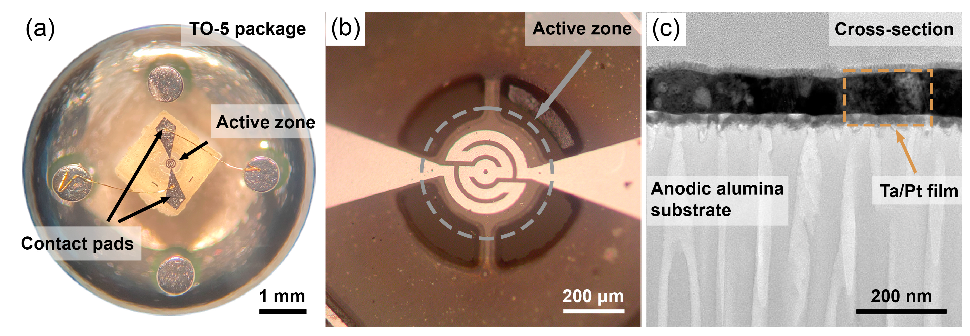
2. Materials and Methods
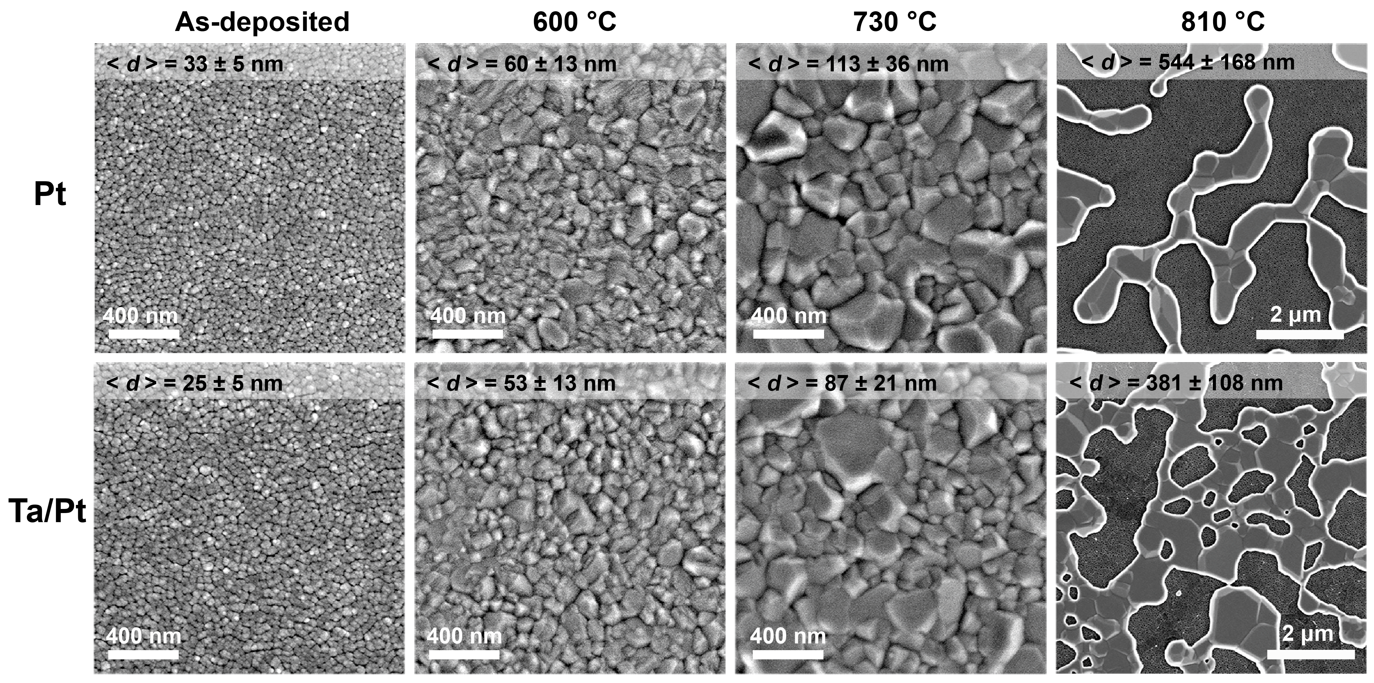
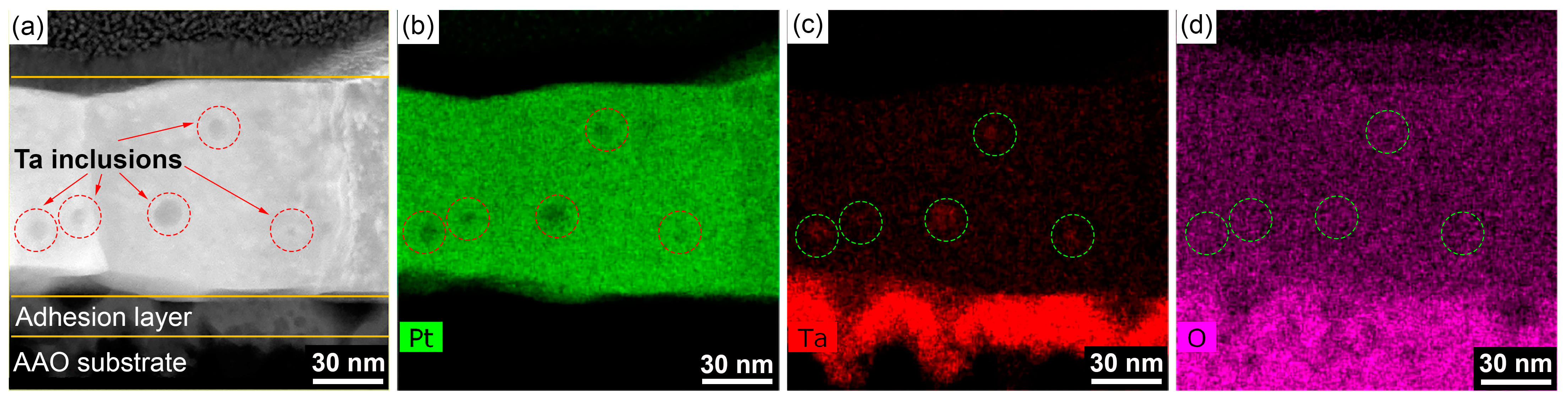
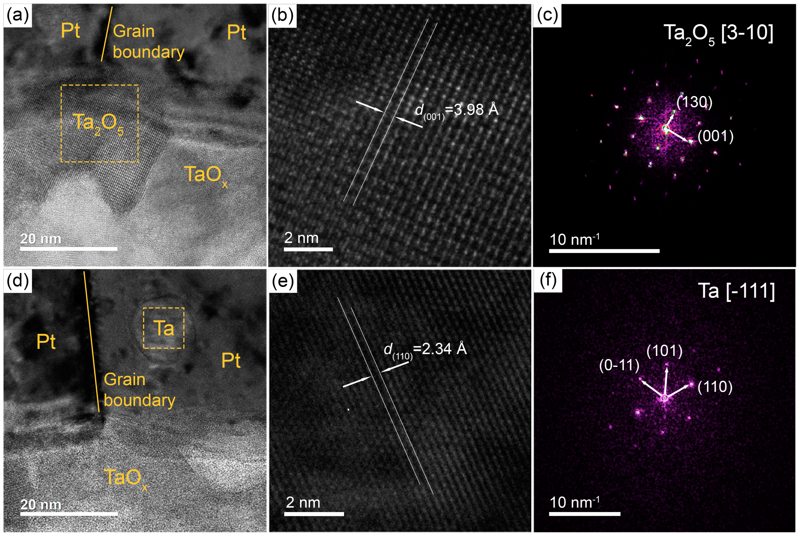
3. Results and Discussion
4. Conclusions
Supplementary Materials
Author Contributions
Funding
Data Availability Statement
Acknowledgments
Conflicts of Interest
References
- Liu, H.; Zhang, L.; Li, K.H.H.; Tan, O.K. Microhotplates for Metal Oxide Semiconductor Gas Sensor Applications—Towards the CMOS-MEMS Monolithic Approach. Micromachines 2018, 9, 557. [Google Scholar] [CrossRef] [PubMed]
- Bhattacharyya, P. Technological Journey towards Reliable Microheater Development for MEMS Gas Sensors: A Review. IEEE Trans. Device Mater. Reliab. 2014, 14, 589–599. [Google Scholar] [CrossRef]
- Karpov, E.E.; Karpov, E.F.; Suchkov, A.; Mironov, S.; Baranov, A.; Sleptsov, V.; Calliari, L. Energy Efficient Planar Catalytic Sensor for Methane Measurement. Sens. Actuators A Phys. 2013, 194, 176–180. [Google Scholar] [CrossRef]
- Roslyakov, I.V.; Kolesnik, I.V.; Evdokimov, P.V.; Skryabina, O.V.; Garshev, A.V.; Mironov, S.M.; Stolyarov, V.S.; Baranchikov, A.E.; Napolskii, K.S. Microhotplate Catalytic Sensors Based on Porous Anodic Alumina: Operando Study of Methane Response Hysteresis. Sens. Actuators B Chem. 2021, 330, 129307. [Google Scholar] [CrossRef]
- Vereshchagina, E.; Tiggelaar, R.M.; Sanders, R.G.P.; Wolters, R.A.M.; Gardeniers, J.G.E. Low Power Micro-Calorimetric Sensors for Analysis of Gaseous Samples. Sens. Actuators B Chem. 2015, 206, 772–787. [Google Scholar] [CrossRef]
- Ejeian, F.; Azadi, S.; Razmjou, A.; Orooji, Y.; Kottapalli, A.; Ebrahimi Warkiani, M.; Asadnia, M. Design and Applications of MEMS Flow Sensors: A Review. Sens. Actuators A Phys. 2019, 295, 483–502. [Google Scholar] [CrossRef]
- Djuzhev, N.A.; Ryabov, V.T.; Demin, G.D.; Makhiboroda, M.A.; Evsikov, I.D.; Pozdnyakov, M.M.; Bespalov, V.A. Measurement System for Wide-Range Flow Evaluation and Thermal Characterization of MEMS-Based Thermoresistive Flow-Rate Sensors. Sens. Actuators A Phys. 2021, 330, 112832. [Google Scholar] [CrossRef]
- Beckel, D.; Briand, D.; Bieberle-Hütter, A.; Courbat, J.; de Rooij, N.F.; Gauckler, L.J. Micro-Hotplates—A Platform for Micro-Solid Oxide Fuel Cells. J. Power Sources 2007, 166, 143–148. [Google Scholar] [CrossRef]
- Podor, R.; Trillaud, V.; Nkou Bouala, G.I.; Dacheux, N.; Ricolleau, C.; Clavier, N. A Multiscale in Situ High Temperature High Resolution Transmission Electron Microscopy Study of ThO 2 Sintering. Nanoscale 2021, 13, 7362–7374. [Google Scholar] [CrossRef]
- van Omme, J.T.; Wu, H.; Sun, H.; Beker, A.F.; Lemang, M.; Spruit, R.G.; Maddala, S.P.; Rakowski, A.; Friedrich, H.; Patterson, J.P.; et al. Liquid Phase Transmission Electron Microscopy with Flow and Temperature Control. J. Mater. Chem. C. Mater. 2020, 8, 10781–10790. [Google Scholar] [CrossRef]
- Spruit, R.G.; Tijn Van Omme, J.; Ghatkesar, M.K.; Hugo Pérez Garza, H. A Review on Development and Optimization of Microheaters for High-Temperature in Situ Studies. J. Microelectromech. Syst. 2017, 26, 1165–1182. [Google Scholar] [CrossRef]
- Lin, X.; Nagl, S. A Microfluidic Chip for Rapid Analysis of DNA Melting Curves for BRCA2 Mutation Screening. Lab Chip 2020, 20, 3824–3831. [Google Scholar] [CrossRef] [PubMed]
- Jang, I.R.; Jung, S.I.; Lee, G.; Park, I.; Kim, S.B.; Kim, H.J. Quartz Crystal Microbalance with Thermally-Controlled Surface Adhesion for an Efficient Fine Dust Collection and Sensing. J. Hazard. Mater. 2022, 424, 127560. [Google Scholar] [CrossRef] [PubMed]
- Liang, G.; Huang, H.; Mohanty, A.; Shin, M.C.; Ji, X.; Carter, M.J.; Shrestha, S.; Lipson, M.; Yu, N. Robust, Efficient, Micrometre-Scale Phase Modulators at Visible Wavelengths. Nat. Photonics 2021, 15, 908–913. [Google Scholar] [CrossRef]
- Zheng, Z.H.; Li, Y.L.; Niu, J.Y.; Wei, M.; Zhang, D.L.; Zhong, Y.M.; Nisar, M.; Abbas, A.; Chen, S.; Li, F.; et al. Significantly (00l)-Textured Ag2Se Thin Films with Excellent Thermoelectric Performance for Flexible Power Applications. J. Mater. Chem. A Mater. 2022, 10, 21603–21610. [Google Scholar] [CrossRef]
- Zheng, Z.H.; Zhang, D.L.; Jabar, B.; Chen, T.B.; Nisar, M.; Chen, Y.F.; Li, F.; Chen, S.; Liang, G.X.; Zhang, X.H.; et al. Realizing High Thermoelectric Performance in Highly (0l0)-Textured Flexible Cu2Se Thin Film for Wearable Energy Harvesting. Mater. Today Phys. 2022, 24, 100659. [Google Scholar] [CrossRef]
- Mele, L.; Santagata, F.; Iervolino, E.; Mihailovic, M.; Rossi, T.; Tran, A.T.; Schellevis, H.; Creemer, J.F.; Sarro, P.M. A Molybdenum MEMS Microhotplate for High-Temperature Operation. Sens. Actuators A Phys. 2012, 188, 173–180. [Google Scholar] [CrossRef]
- Zhang, K.L.; Chou, S.K.; Ang, S.S. Fabrication, Modeling and Testing of a Thin Film Au/Ti Microheater. Int. J. Therm. Sci. 2007, 46, 580–588. [Google Scholar] [CrossRef]
- Ricci, P.P.; Gregory, O.J. Free-Standing, Thin-Film Sensors for the Trace Detection of Explosives. Sci. Rep. 2021, 11, 6623. [Google Scholar] [CrossRef]
- Wu, J.; Wu, Z.; Ding, H.; Wei, Y.; Yang, X.; Li, Z.; Yang, B.R.; Liu, C.; Qiu, L.; Wang, X. Multifunctional and High-Sensitive Sensor Capable of Detecting Humidity, Temperature, and Flow Stimuli Using an Integrated Microheater. ACS Appl. Mater. Interfaces 2019, 11, 43383–43392. [Google Scholar] [CrossRef]
- Creemer, J.F.; Briand, D.; Zandbergen, H.W.; van der Vlist, W.; de Boer, C.R.; de Rooij, N.F.; Sarro, P.M. Microhotplates with TiN Heaters. Sens. Actuators A Phys. 2008, 148, 416–421. [Google Scholar] [CrossRef]
- Jithin, M.A.; Kolla, L.G.; Vikram, G.N.V.R.; Udayashankar, N.K.; Mohan, S. Pulsed DC Magnetron Sputtered Titanium Nitride Thin Films for Localized Heating Applications in MEMS Devices. Sens. Actuators A Phys. 2018, 272, 199–205. [Google Scholar] [CrossRef]
- Long, H.; Harley-Trochimczyk, A.; He, T.; Pham, T.; Tang, Z.; Shi, T.; Zettl, A.; Mickelson, W.; Carraro, C.; Maboudian, R. In Situ Localized Growth of Porous Tin Oxide Films on Low Power Microheater Platform for Low Temperature CO Detection. ACS Sens. 2016, 1, 339–343. [Google Scholar] [CrossRef]
- Jung, G.; Hong, Y.; Hong, S.; Jang, D.; Jeong, Y.; Shin, W.; Park, J.; Kim, D.; Jeong, C.B.; Kim, D.U.; et al. A Low-Power Embedded Poly-Si Micro-Heater for Gas Sensor Platform Based on a FET Transducer and Its Application for NO2 Sensing. Sens. Actuators B Chem. 2021, 334, 129642. [Google Scholar] [CrossRef]
- Lide, D.R. Hardness of Minerals and Ceramics. In CRC Handbook of Chemistry and Physics; CRC Press LLC: Boca Raton, FL, USA, 2004. [Google Scholar]
- Ma, D.; Mao, S.; Teng, J.; Wang, X.; Li, X.; Ning, J.; Li, Z.; Zhang, Q.; Tian, Z.; Wang, M.; et al. In-Situ Revealing the Degradation Mechanisms of Pt Film over 1000 °C. J. Mater. Sci. Technol. 2021, 95, 10–19. [Google Scholar] [CrossRef]
- Puigcorbé, J.; Vogel, D.; Michel, B.; Vilà, A.; Gracia, I.; Cané, C.; Morante, J.R. High Temperature Degradation of Pt/Ti Electrodes in Micro-Hotplate Gas Sensors. J. Micromechanics Microeng 2003, 13, S119. [Google Scholar] [CrossRef]
- Lee, A.; Clemens, B.M.; Nix, W.D. Stress Induced Delamination Methods for the Study of Adhesion of Pt Thin Films to Si. Acta Mater. 2004, 52, 2081–2093. [Google Scholar] [CrossRef]
- Schössler, T.; Schön, F.; Lemier, C.; Urban, G. Effect of High Temperature Annealing on Resistivity and Temperature Coefficient of Resistance of Sputtered Platinum Thin Films of SiO2/Pt/SiOx Interfaces. Thin Solid Films 2020, 698, 137877. [Google Scholar] [CrossRef]
- Idczak, K.; Owczarek, S.; Markowski, L. Platinum Silicide Formation on Selected Semiconductors Surfaces via Thermal Annealing and Intercalation. Appl. Surf. Sci. 2022, 572, 151345. [Google Scholar] [CrossRef]
- Kim, J.Y.; Lee, J.H.; Kim, J.H.; Mirzaei, A.; Woo Kim, H.; Kim, S.S. Realization of H2S Sensing by Pd-Functionalized Networked CuO Nanowires in Self-Heating Mode. Sens. Actuators B Chem. 2019, 299, 126965. [Google Scholar] [CrossRef]
- Steinhauer, S.; Chapelle, A.; Menini, P.; Sowwan, M. Local CuO Nanowire Growth on Microhotplates: In Situ Electrical Measurements and Gas Sensing Application. ACS Sens. 2016, 1, 503–507. [Google Scholar] [CrossRef]
- Meyer, R.; Hamann, S.; Ehmann, M.; Thienhaus, S.; Jaeger, S.; Thiede, T.; Devi, A.; Fischer, R.A.; Ludwig, A. Microgradient-Heaters As Tools for High-Throughput Experimentation. ACS Comb. Sci. 2012, 14, 531–536. [Google Scholar] [CrossRef] [PubMed]
- Sun, J.; Liu, Z.; Zhang, S.; Zhan, T.; Wang, J.; Yi, X.; Li, J.; Sarro, P.M.; Zhang, G. A High Responsivity and Controllable Recovery Ultraviolet Detector Based on a WO 3 Gate AlGaN/GaN Heterostructure with an Integrated Micro-Heater. J. Mater. Chem. C 2020, 8, 5409–5416. [Google Scholar] [CrossRef]
- Esch, H.; Huyberechts, G.; Mertens, R.; Maes, G.; Manca, J.; de Ceuninck, W.; de Schepper, L. The Stability of Pt Heater and Temperature Sensing Elements for Silicon Integrated Tin Oxide Gas Sensors. Sens. Actuators B Chem. 2000, 65, 190–192. [Google Scholar] [CrossRef]
- Phan, D.T.; Youn, J.S.; Jeon, K.J. High-Sensitivity and Fast-Response Hydrogen Sensor for Safety Application Using Pt Nanoparticle-Decorated 3D Graphene. Renew Energy 2019, 144, 167–171. [Google Scholar] [CrossRef]
- del Orbe, D.v.; Yang, H.; Cho, I.; Park, J.; Choi, J.; Han, S.W.; Park, I. Low-Power Thermocatalytic Hydrogen Sensor Based on Electrodeposited Cauliflower-like Nanostructured Pt Black. Sens. Actuators B Chem. 2021, 329, 129129. [Google Scholar] [CrossRef]
- Wang, X.S.; Wang, Y.J.; Yin, J.; Liu, Z.G. Enhanced Ferroelectric Properties of Pb (Zr0. 52Ti0. 48) O3 films on Pt/TiO2/SiO2/Si (001) using ZnO Buffer Layer. Scr. Mater. 2002, 46, 783–787. [Google Scholar] [CrossRef]
- DiBattista, M.; Schwank, J.W. Determination of Diffusion in Polycrystalline Platinum Thin Films. J. Appl. Phys. 1999, 86, 4902. [Google Scholar] [CrossRef]
- Resnik, D.; Kovač, J.; Vrtačnik, D.; Godec, M.; Pečar, B.; Možek, M. Microstructural and Electrical Properties of Heat Treated Resistive Ti/Pt Thin Layers. Thin Solid Films 2017, 639, 64–72. [Google Scholar] [CrossRef]
- Grosser, M.; Schmid, U. The Impact of Annealing Temperature and Time on the Electrical Performance of Ti/Pt Thin Films. Appl. Surf. Sci. 2010, 256, 4564–4569. [Google Scholar] [CrossRef]
- Schmid, U. The Impact of Thermal Annealing and Adhesion Film Thickness on the Resistivity and the Agglomeration Behavior of Titanium/Platinum Thin Films. J. Appl. Phys. 2008, 103, 054902. [Google Scholar] [CrossRef]
- Varniere, F.; Kim, B.E.; Agius, B.; Bisaro, R.; Olivier, J.; Chevrier, G.; Achard, H.; Mace, H.; Peccoud, L. Effects of Annealings on Pt/TiN/Ti Interfacial Reactions. MRS Online Proc. Libr. 1994, 361, 235–240. [Google Scholar] [CrossRef]
- Ehrlich, A.; Weiß, U.; Hoyer, W.; Geßner, T. Microstructural Changes of Pt/Ti Bilayer during Annealing in Different Atmospheres—An XRD Study. Thin Solid Films 1997, 300, 122–130. [Google Scholar] [CrossRef]
- Jones, J.L.; LeBeau, J.M.; Nikkel, J.; Oni, A.A.; Dycus, J.H.; Cozzan, C.; Lin, F.Y.; Chernatynskiy, A.; Nino, J.C.; Sinnott, S.B.; et al. Combined Experimental and Computational Methods Reveal the Evolution of Buried Interfaces during Synthesis of Ferroelectric Thin Films. Adv. Mater. Interfaces 2015, 2, 1500181. [Google Scholar] [CrossRef]
- Garraud, A.; Combette, P.; Giani, A. Thermal Stability of Pt/Cr and Pt/Cr2O3 Thin-Film Layers on a SiNx/Si Substrate for Thermal Sensor Applications. Thin Solid Films 2013, 540, 256–260. [Google Scholar] [CrossRef]
- Frankel, D.J.; Moulzolf, S.C.; da Cunha, M.P.; Lad, R.J. Influence of Composition and Multilayer Architecture on Electrical Conductivity of High Temperature Pt-Alloy Films. Surf. Coat. Technol. 2015, 284, 215–221. [Google Scholar] [CrossRef]
- Schmid, P.; Zarfl, C.; Triendl, F.; Maier, F.J.; Schwarz, S.; Schneider, M.; Schmid, U. Impact of Adhesion Promoters and Sputter Parameters on the Electro-Mechanical Properties of Pt Thin Films at High Temperatures. Sens. Actuators A Phys. 2019, 285, 149–157. [Google Scholar] [CrossRef]
- Çiftyürek, E.; Sabolsky, K.; Sabolsky, E.M. Platinum Thin Film Electrodes for High-Temperature Chemical Sensor Applications. Sens. Actuators B Chem. 2013, 181, 702–714. [Google Scholar] [CrossRef]
- Moulzolf, S.C.; Frankel, D.J.; Pereira Da Cunha, M.; Lad, R.J. High Temperature Stability of Electrically Conductive Pt-Rh/ZrO 2 and Pt-Rh/HfO 2 Nanocomposite Thin Film Electrodes. Microsyst. Technol. 2014, 20, 523–531. [Google Scholar] [CrossRef]
- Çiftyürek, E.; McMillen, C.D.; Sabolsky, K.; Sabolsky, E.M. Platinum–Zirconium Composite Thin Film Electrodes for High-Temperature Micro-Chemical Sensor Applications. Sens. Actuators B Chem. 2015, 207, 206–215. [Google Scholar] [CrossRef]
- Alonso, P.R.; Arias, D.E.; Gribaudo, L.M. The Zr-Rich Zone in the Zr-Pt System. Scr. Mater. 2001, 44, 429–434. [Google Scholar] [CrossRef]
- Wöllenstein, J.; Plaza, J.A.; Cané, C.; Min, Y.; Böttner, H.; Tuller, H.L. A Novel Single Chip Thin Film Metal Oxide Array. Sens. Actuators B Chem. 2003, 93, 350–355. [Google Scholar] [CrossRef]
- Grassi, M.; Malcovati, P.; Francioso, L.; Siciliano, P.; Baschirotto, A. Integrated Interface Circuit with Multiplexed Input and Digital Output for a 5 × 5 SnO2 Thick Film Gas-Sensor Matrix. Sens. Actuators B Chem. 2008, 132, 568–575. [Google Scholar] [CrossRef]
- Bose, A.; Shukla, A.S.; Dutta, S.; Bhuktare, S.; Singh, H.; Tulapurkar, A.A. Control of Magnetization Dynamics by Spin-Nernst Torque. APS 2018, 98, 184412. [Google Scholar] [CrossRef]
- Wang, Z.; Guo, M.; Zhou, H.A.; Zhao, L.; Xu, T.; Tomasello, R.; Bai, H.; Dong, Y.; Je, S.G.; Chao, W.; et al. Thermal Generation, Manipulation and Thermoelectric Detection of Skyrmions. Nat. Electron. 2020, 3, 672–679. [Google Scholar] [CrossRef]
- Firebaugh, S.L.; Jensen, K.F.; Schmidt, M.A. Investigation of High-Temperature Degradation of Platinum Thin Films with an in Situ Resistance Measurement Apparatus. J. Microelectromech. Syst. 1998, 7, 128–135. [Google Scholar] [CrossRef]
- Gardeniers, J.G.E.; Tjerkstra, R.W.; Berg, A. van den Fabrication and Application of Silicon-Based Microchannels. Microreact. Technol. Ind. Prospect. 2000, 1, 36–44. [Google Scholar] [CrossRef]
- Courbat, J.; Briand, D.; de Rooij, N.F. Reliability Improvement of Suspended Platinum-Based Micro-Heating Elements. Sens. Actuators A Phys. 2008, 142, 284–291. [Google Scholar] [CrossRef]
- Tiggelaar, R.M.; Sanders, R.G.P.; Groenland, A.W.; Gardeniers, J.G.E. Stability of Thin Platinum Films Implemented in High-Temperature Microdevices. Sens. Actuators A Phys. 2009, 152, 39–47. [Google Scholar] [CrossRef]
- Vasiliev, A.A.; Pisliakov, A.V.; Sokolov, A.V.; Samotaev, N.N.; Soloviev, S.A.; Oblov, K.; Guarnieri, V.; Lorenzelli, L.; Brunelli, J.; Maglione, A.; et al. Non-Silicon MEMS Platforms for Gas Sensors. Sens. Actuators B Chem. 2016, 224, 700–713. [Google Scholar] [CrossRef]
- Kalinin, I.A.; Roslyakov, I.V.; Tsymbarenko, D.M.; Bograchev, D.A.; Krivetskiy, V.V.; Napolskii, K.S. Microhotplates Based on Pt and Pt-Rh Films: The Impact of Composition, Structure, and Thermal Treatment on Functional Properties. Sens. Actuators A Phys. 2021, 317, 112457. [Google Scholar] [CrossRef]
- Roslyakov, I.V.; Sotnichuk, S.V.; Kushnir, S.E.; Trusov, L.A.; Bozhev, I.V.; Napolskii, K.S. Pore Ordering in Anodic Aluminum Oxide: Interplay between the Pattern of Pore Nuclei and the Crystallographic Orientation of Aluminum. Nanomaterials 2022, 12, 1417. [Google Scholar] [CrossRef] [PubMed]
- Hermetic Packages for Integrated Circuits (Glass-to-Metal Seals Packages). Available online: http://www.z-mars.ru/en/?category=101 (accessed on 19 November 2022).
- Schneider, C.A.; Rasband, W.S.; Eliceiri, K.W. NIH Image to ImageJ: 25 Years of Image Analysis. Nat. Methods 2012, 9, 671–675. [Google Scholar] [CrossRef] [PubMed]
- Dey, A. Semiconductor Metal Oxide Gas Sensors: A Review. Mater. Sci. Eng. B 2018, 229, 206–217. [Google Scholar] [CrossRef]
- Ababneh, A.; Al-Omari, A.N.; Dagamseh, A.M.K.; Tantawi, M.; Pauly, C.; Mücklich, F.; Feili, D.; Seidel, H. Electrical and Morphological Characterization of Platinum Thin-Films with Various Adhesion Layers for High Temperature Applications. Microsyst. Technol. 2017, 23, 703–709. [Google Scholar] [CrossRef]
- Abbas, W.; Lin, W.; Kai, J.J.; Ho, D.; Pramanick, A. Critical Effect of Film-Electrode Interface on Enhanced Energy Storage Performance of BaTiO3-BiScO3 Ferroelectric Thin Films. ACS Appl. Electron. Mater. 2021, 3, 4726–4733. [Google Scholar] [CrossRef]
- Nečas, D.; Klapetek, P. Gwyddion: An Open-Source Software for SPM Data Analysis. Open Phys. 2012, 10, 181–188. [Google Scholar] [CrossRef]
- Maeder, T.; Sagalowicz, L.; Muralt, P. Stabilized Platinum Electrodes for Ferroelectric Film Deposition Using Ti, Ta and Zr Adhesion Layers. Jpn. J. Appl. Phys. 1998, 37, 2007–2012. [Google Scholar] [CrossRef]
- Briand, D.; Heimgartner, S.; Leboeuf, M.; Dadras, M.; de Rooij, N.F. Processing Influence on the Reliability of Platinum Thin Films for MEMS Applications. MRS Online Proc. Libr. 2002, 729, 25. [Google Scholar] [CrossRef]


| Characteristic | As-Deposited | 600 °C | 730 °C | 810 °C | ||||
|---|---|---|---|---|---|---|---|---|
| Pt | Ta/Pt | Pt | Ta/Pt | Pt | Ta/Pt | Pt | Ta/Pt | |
| Resistance, Ω | 131 ± 1 | 86 ± 4 | 73 ± 3 | 66 ± 1 | 68 ± 5 | 69 ± 4 | - | 97 ± 10 |
| TCR (×103), ppm/°C | 1.5 ± 0.1 | 2.0 ± 0.1 | 2.8 ± 0.1 | 3.1 ± 0.1 | 3.1 ± 0.3 | 3.1 ± 0.2 | - | 3.3 ± 0.3 |
| Power consumption at 500 °C, mW | - | - | 101 ± 3 | 120 ± 17 | 99 ± 5 | 113 ± 10 | - | 101 ± 8 |
| Supply voltage (500 °C), V | - | - | 4.3 ± 0.1 | 4.4 ± 0.3 | 4.0 ± 0.1 | 4.4 ± 0.3 | - | 5.1 ± 0.2 |
| Resistance drift, %/day | - | - | - | 0.19 ± 0.14 | - | 0.09 ± 0.03 | - | 0.17 ± 0.07 |
Disclaimer/Publisher’s Note: The statements, opinions and data contained in all publications are solely those of the individual author(s) and contributor(s) and not of MDPI and/or the editor(s). MDPI and/or the editor(s) disclaim responsibility for any injury to people or property resulting from any ideas, methods, instructions or products referred to in the content. |
© 2022 by the authors. Licensee MDPI, Basel, Switzerland. This article is an open access article distributed under the terms and conditions of the Creative Commons Attribution (CC BY) license (https://creativecommons.org/licenses/by/4.0/).
Share and Cite
Kalinin, I.A.; Roslyakov, I.V.; Khmelenin, D.N.; Napolskii, K.S. Long-Term Operational Stability of Ta/Pt Thin-Film Microheaters: Impact of the Ta Adhesion Layer. Nanomaterials 2023, 13, 94. https://doi.org/10.3390/nano13010094
Kalinin IA, Roslyakov IV, Khmelenin DN, Napolskii KS. Long-Term Operational Stability of Ta/Pt Thin-Film Microheaters: Impact of the Ta Adhesion Layer. Nanomaterials. 2023; 13(1):94. https://doi.org/10.3390/nano13010094
Chicago/Turabian StyleKalinin, Ivan A., Ilya V. Roslyakov, Dmitry N. Khmelenin, and Kirill S. Napolskii. 2023. "Long-Term Operational Stability of Ta/Pt Thin-Film Microheaters: Impact of the Ta Adhesion Layer" Nanomaterials 13, no. 1: 94. https://doi.org/10.3390/nano13010094
APA StyleKalinin, I. A., Roslyakov, I. V., Khmelenin, D. N., & Napolskii, K. S. (2023). Long-Term Operational Stability of Ta/Pt Thin-Film Microheaters: Impact of the Ta Adhesion Layer. Nanomaterials, 13(1), 94. https://doi.org/10.3390/nano13010094