
Vanadium and Manganese Carbonyls as Precursors in Electron-Induced and Thermal Deposition Processes

 , , , and
Abstract
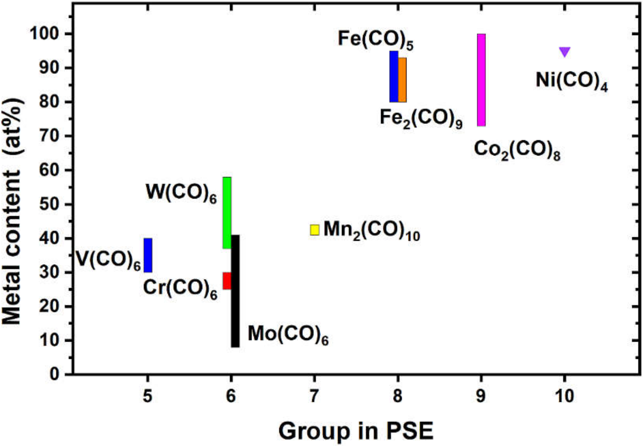
1. Introduction
2. Materials and Methods
2.1. Precursor Preparation/Synthesis
2.2. FEBID Process
2.3. Transport Measurements and Compositional Analysis
3. Results and Discussion
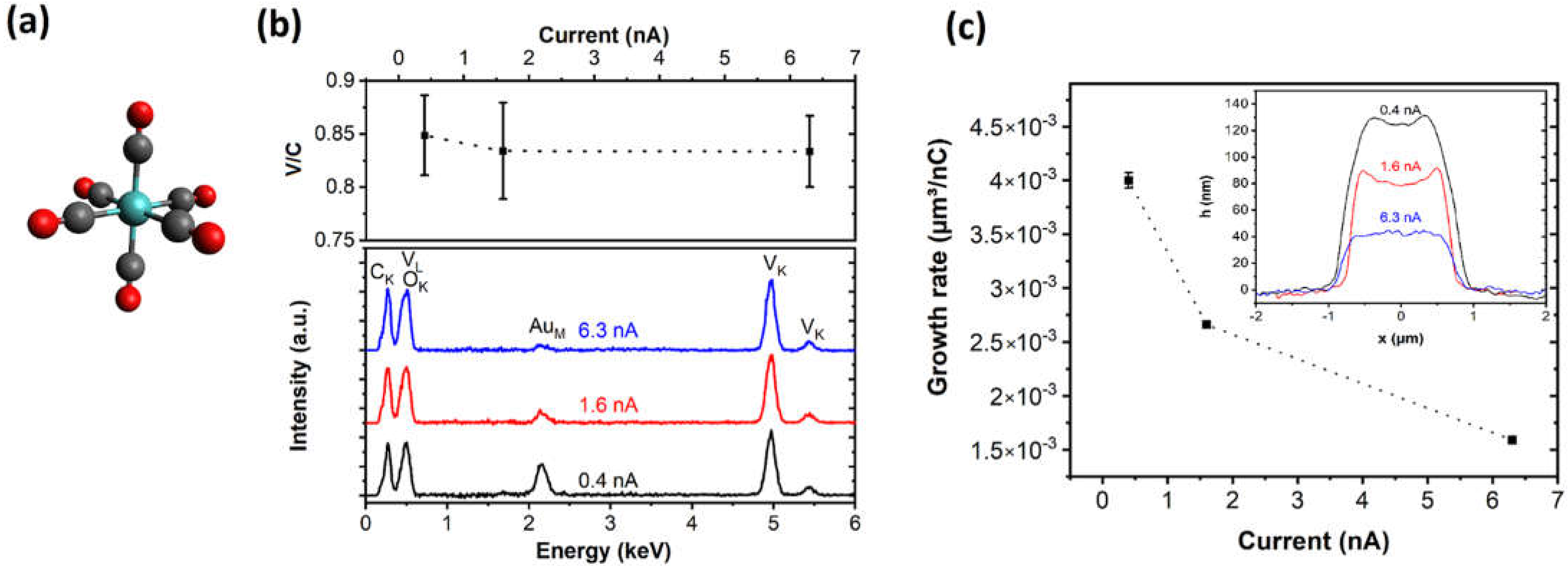
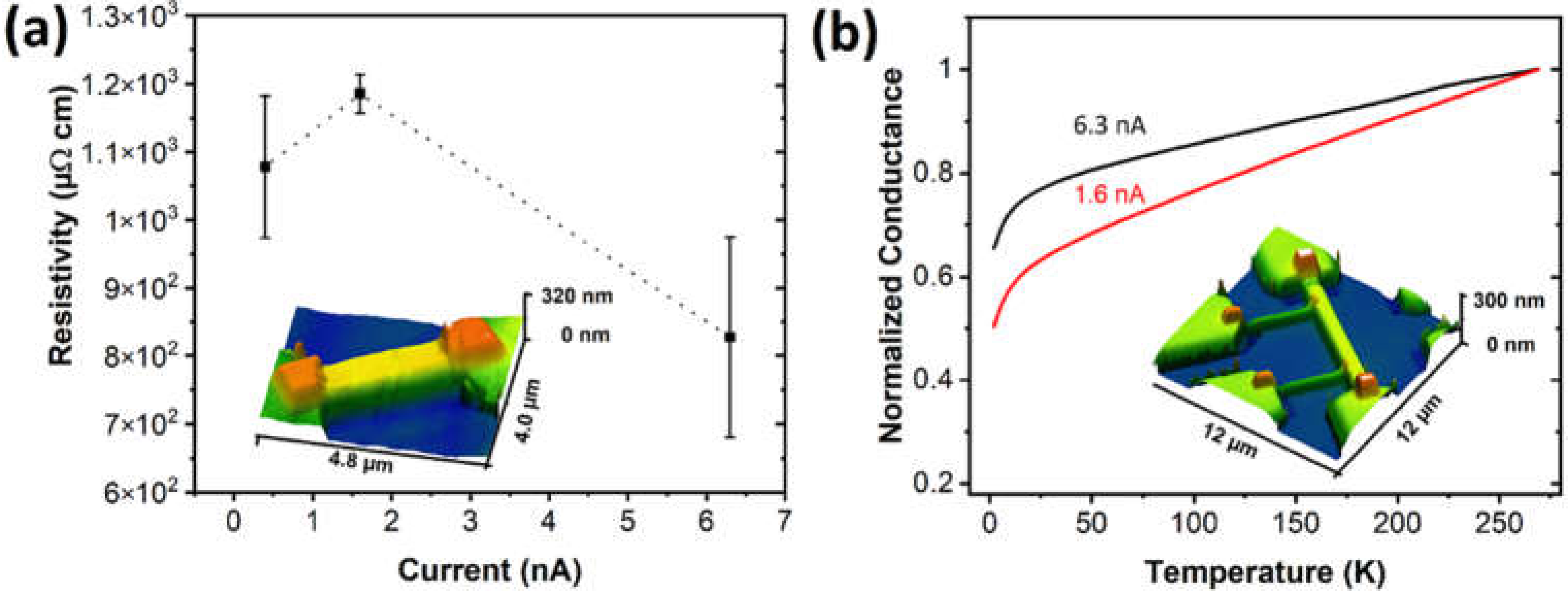
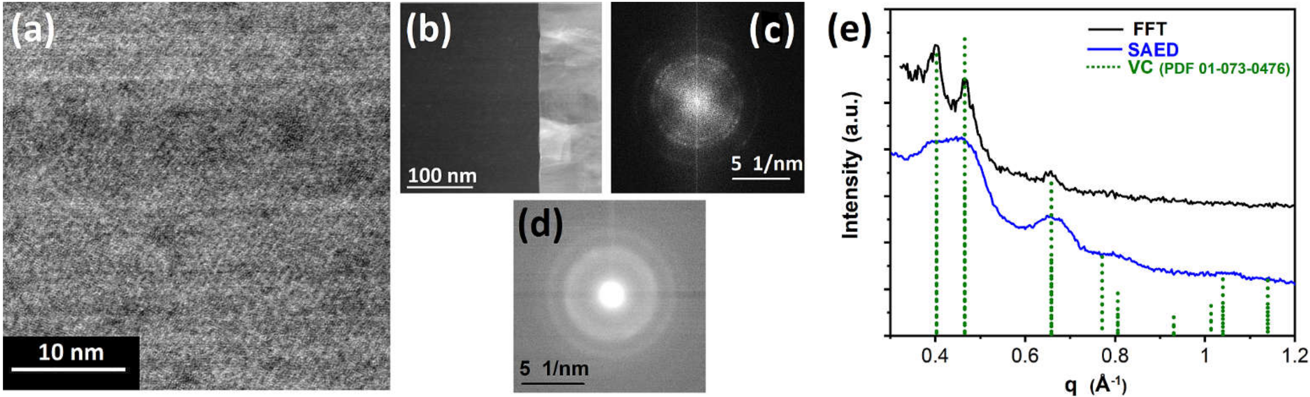
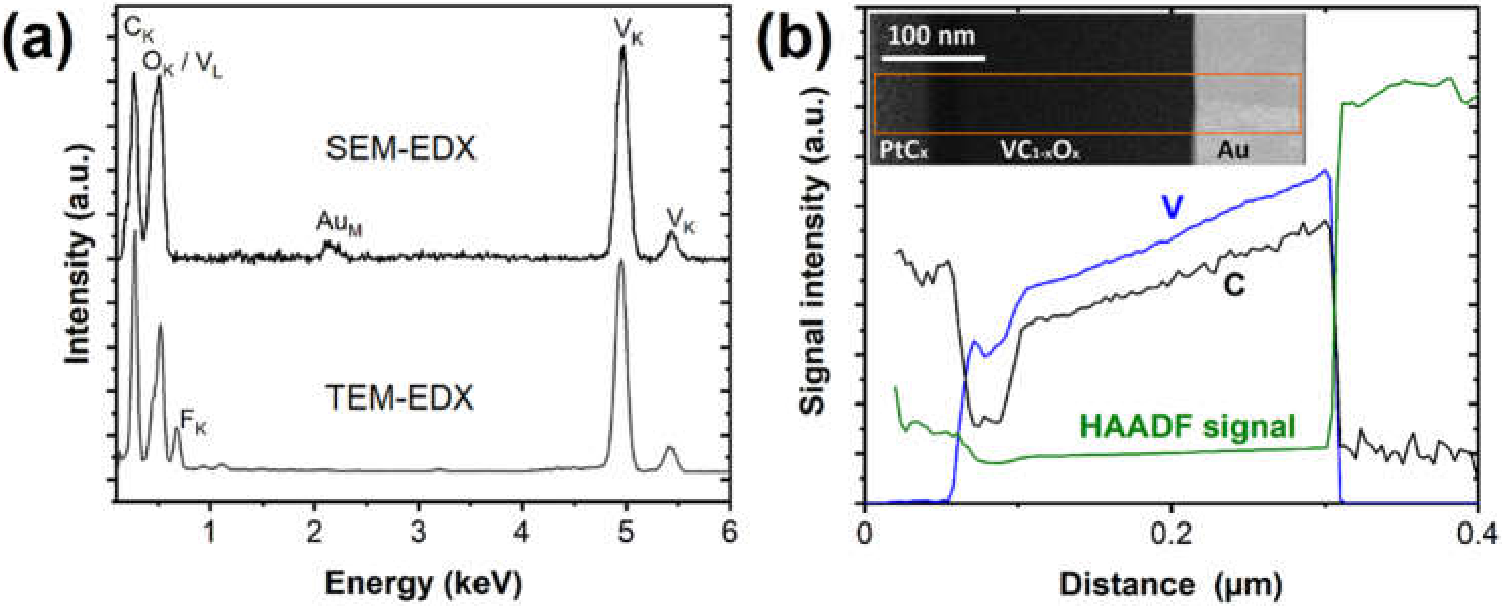
3.1. Vanadium Carbonyl Precursor
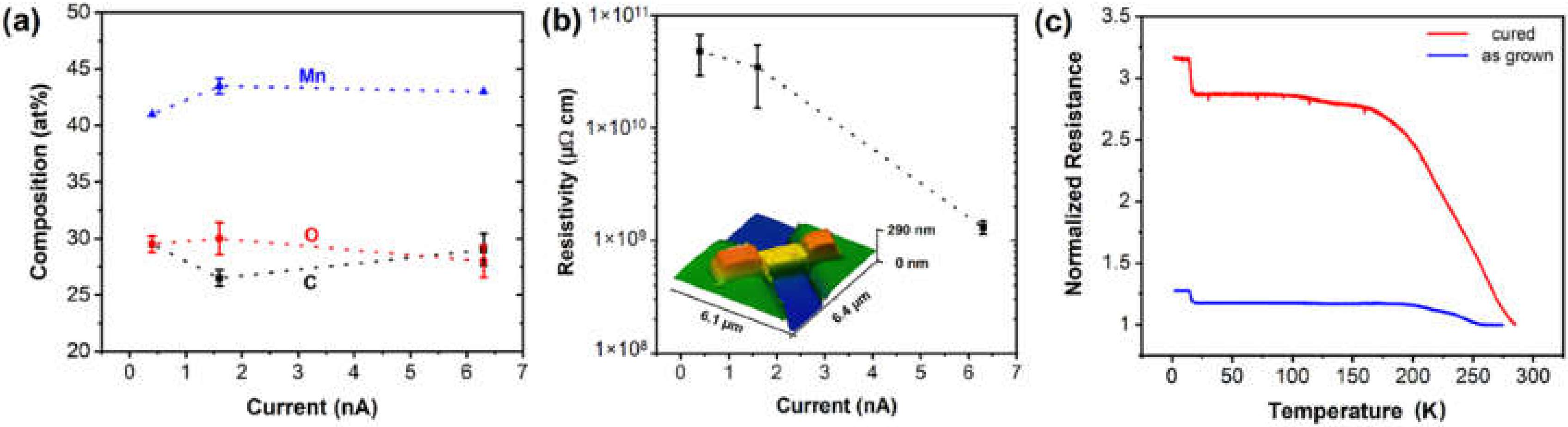
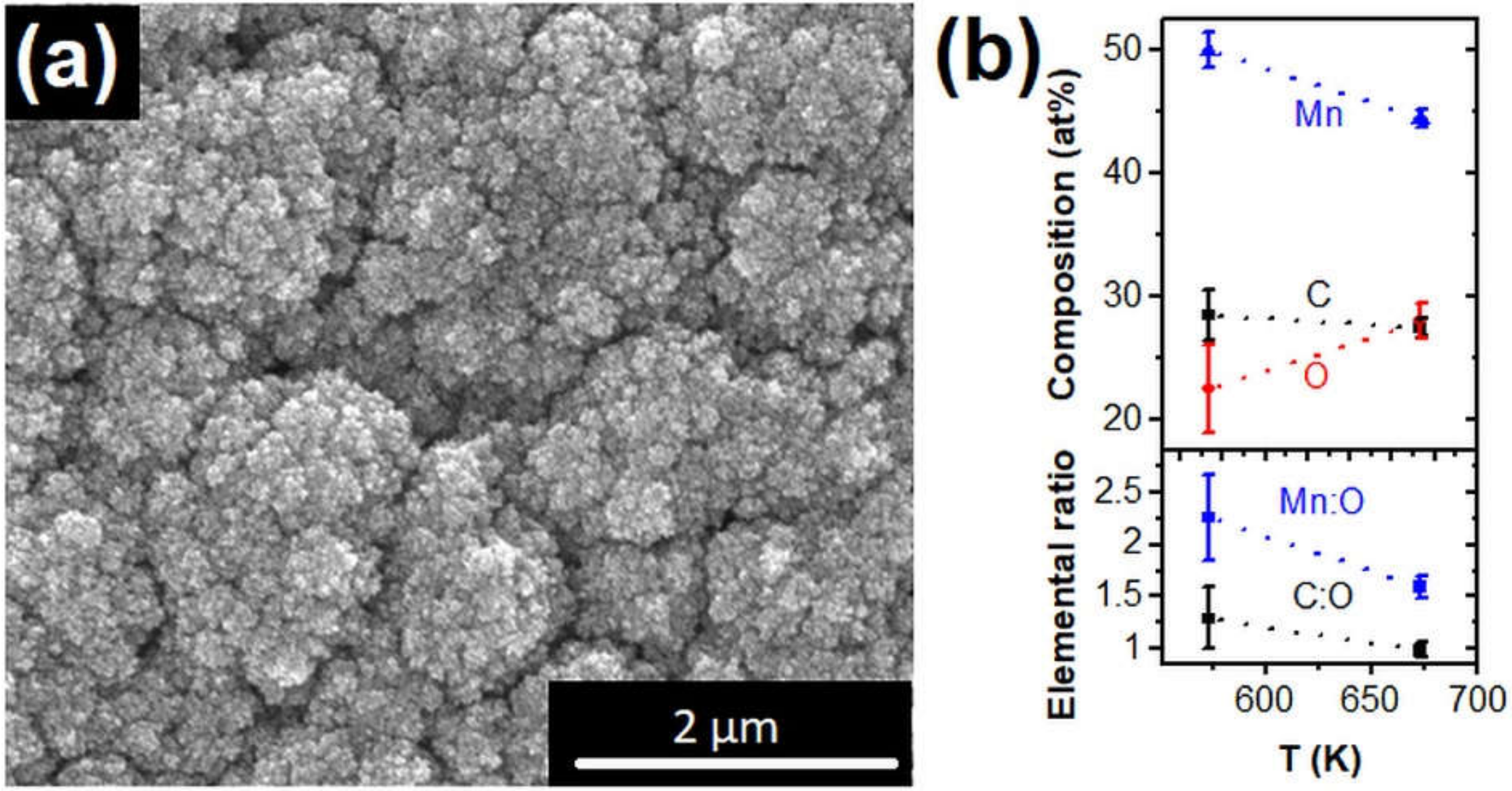
3.2. Manganese Carbonyl Precursor
3.3. Carbonyl Precursors in FEBID
4. Conclusions
Supplementary Materials
Author Contributions
Funding
Institutional Review Board Statement
Informed Consent Statement
Data Availability Statement
Acknowledgments
Conflicts of Interest
References
- Hari, S.; Verduin, T.; Kruit, P.; Hagen, C.W. A study of the reproducibility of electron beam induced deposition for sub-20 nm lithography. Micro Nano Eng. 2019, 4, 1–6. [Google Scholar] [CrossRef]
- Huth, M.; Porrati, F.; Dobrovolskiy, O.V. Focused Electron Beam Induced Deposition Meets Materials Science. Microelectron. Eng. 2018, 185–186, 9–28. [Google Scholar] [CrossRef]
- Utke, I.; Hoffmann, P.; Melngailis, J. Gas-Assisted Focused Electron Beam and Ion Beam Processing and Fabrication. J. Vac. Sci. Technol. B 2008, 26, 1197–1276. [Google Scholar] [CrossRef]
- De Teresa, J.M.; Fernández-Pacheco, A.; Córdoba, R.; Serrano-Ramón, L.; Sangiao, S.; Ibarra, M.R. Review of Magnetic Nanostructures Grown by Focused Electron Beam Induced Deposition (FEBID). J. Phys. D Appl. Phys. 2016, 49, 243003. [Google Scholar] [CrossRef]
- Huth, M.; Porrati, F.; Barth, S. Living up to its potential—Direct-write nanofabrication with focused electron beams. J. Appl. Phys. 2021, 130, 170901. [Google Scholar] [CrossRef]
- Plank, H.; Winkler, R.; Schwalb, C.H.; Hütner, J.; Fowlkes, J.D.; Rack, P.D.; Utke, I.; Huth, M. Focused Electron Beam-Based 3D Nanoprinting for Scanning Probe Microscopy: A Review. Micromachines 2019, 11, 48. [Google Scholar] [CrossRef]
- Dobrovolskiy, O.V.; Vovk, N.R.; Bondarenko, A.V.; Bunyaev, S.A.; Lamb-Camarena, S.; Zenbaa, N.; Sachser, R.; Barth, S.; Guslienko, K.Y.; Chumak, A.V.; et al. Spin-wave eigenmodes in direct-write 3D nanovolcanoes. Appl. Phys. Lett. 2021, 118, 132405. [Google Scholar] [CrossRef]
- Dukic, M.; Winhold, M.; Schwalb, C.H.; Adams, J.D.; Stavrov, V.; Huth, M.; Fantner, G.E. Direct-write nanoscale printing of nanogranular tunnelling strain sensors for sub-micrometre cantilevers. Nat. Commun. 2016, 7, 12487. [Google Scholar] [CrossRef] [PubMed]
- Arnold, G.; Winkler, R.; Stermitz, M.; Orthacker, A.; Noh, J.-H.; Fowlkes, J.D.; Kothleitner, G.; Huth, M.; Rack, P.D.; Plank, H. Tunable 3D Nanoresonators for Gas-Sensing Applications. Adv. Funct. Mater. 2018, 28, 1707387. [Google Scholar] [CrossRef]
- Barth, S.; Huth, M.; Jungwirth, F. Precursors for direct-write nanofabrication with electrons. J. Mater. Chem. C 2020, 8, 15884–15919. [Google Scholar] [CrossRef]
- Carden, W.G.; Lu, H.; Spencer, J.A.; Fairbrother, D.H.; McElwee-White, L. Mechanism-Based Design of Precursors for Focused Electron Beam-Induced Deposition. MRS Commun. 2018, 8, 343–357. [Google Scholar] [CrossRef]
- Rodríguez, L.A.; Deen, L.; Córdoba, R.; Magén, C.; Snoeck, E.; Koopmans, B.; De Teresa, J.M. Influence of the Shape and Surface Oxidation in the Magnetization Reversal of Thin Iron Nanowires Grown by Focused Electron Beam Induced Deposition. Beilstein J. Nanotechnol. 2015, 6, 1319–1331. [Google Scholar] [CrossRef] [PubMed]
- Córdoba, R.; Sharma, N.; Kölling, S.; Koenraad, P.M.; Koopmans, B. High-Purity 3D Nano-Objects Grown by Focused-Electron-Beam Induced Deposition. Nanotechnology 2016, 27, 355301. [Google Scholar] [CrossRef] [PubMed]
- Keller, L.; Al Mamoori, M.K.I.; Pieper, J.; Gspan, C.; Stockem, I.; Schröder, C.; Barth, S.; Winkler, R.; Plank, H.; Pohlit, M.; et al. Direct-Write of Free-Form Building Blocks for Artificial Magnetic 3D Lattices. Sci. Rep. 2018, 8, 6160. [Google Scholar] [CrossRef] [PubMed]
- Porrati, F.; Pohlit, M.; Müller, J.; Barth, S.; Biegger, F.; Gspan, C.; Plank, H.; Huth, M. Direct Writing of CoFe Alloy Nanostructures by Focused Electron Beam Induced Deposition from a Heteronuclear Precursor. Nanotechnology 2015, 26, 475701. [Google Scholar] [CrossRef] [PubMed]
- Luo, Y.-R. Comprehensive Handbook of Chemical Bond Energies; Taylor & Francis: Boca Raton, FL, USA, 2007; p. 1688. [Google Scholar]
- Laporta, V.; Tennyson, J.; Celiberto, R. Carbon monoxide dissociative attachment and resonant dissociation by electron-impact. Plasma Sources Sci. Technol. 2016, 25, 01LT04. [Google Scholar] [CrossRef][Green Version]
- Andreoni, W.; Varma, C.M. Binding and Dissociation of CO on Transition-Metal Surfaces. Phys. Rev. B 1981, 23, 437–444. [Google Scholar] [CrossRef]
- Ramsier, R.D.; Henderson, M.A.; Yates, J.T. Electron Induced Decomposition of Ni(CO)4 Adsorbed on Ag(111). Surf. Sci. 1991, 257, 9–21. [Google Scholar] [CrossRef]
- Henderson, M.A.; Ramsier, R.D.; Yates, J.T. Low-Energy Electron Induced Decomposition of Fe(CO)5 Adsorbed on Ag(111). Surf. Sci. 1991, 259, 173–182. [Google Scholar] [CrossRef]
- TP, R.K.; Unlu, I.; Barth, S.; Ingólfsson, O.; Fairbrother, D.H. Electron Induced Surface Reactions of HFeCo3(CO)12, a Bimetallic Precursor for Focused Electron Beam Induced Deposition (FEBID). J. Phys. Chem. C 2018, 122, 2648–2660. [Google Scholar] [CrossRef]
- Belova, L.M.; Dahlberg, E.D.; Riazanova, A.; Mulders, J.J.L.; Christophersen, C.; Eckert, J. Rapid Electron Beam Assisted Patterning of Pure Cobalt at Elevated Temperatures via Seeded Growth. Nanotechnology 2011, 22, 145305. [Google Scholar] [CrossRef]
- Mulders, J.J.L.; Belova, L.M.; Riazanova, A. Electron Beam Induced Deposition at Elevated Temperatures: Compositional Changes and Purity Improvement. Nanotechnology 2010, 22, 055302. [Google Scholar] [CrossRef] [PubMed]
- Utke, I.; Swiderek, P.; Höflich, K.; Madajska, K.; Jurczyk, J.; Martinović, P.; Szymańska, I.B. Coordination and organometallic precursors of group 10 and 11 Focused electron beam induced deposition of metals and insight gained from chemical vapour deposition, atomic layer deposition, and fundamental surface and gas phase studies. Coord. Chem. Rev. 2022, 458, 213851. [Google Scholar] [CrossRef]
- Liu, X.; Ellis, J.E.; Mesaros, E.F.; Pearson, A.J.; Schoffers, E.; Hall, J.M.; Hoyne, J.H.; Shapley, J.R.; Fauré, M.; Saccavini, C.; et al. Transition Metal Carbonyl Compounds. In Inorganic Syntheses; John Wiley & Sons, Inc.: Hoboken, NJ, USA, 2004; pp. 96–132. [Google Scholar]
- Mathur, S.; Barth, S.; Shen, H. Chemical Vapor Growth of NiGa2O4 Films: Advantages and Limitations of a Single Molecular Source. Chem. Vapor Depos. 2005, 11, 11–16. [Google Scholar] [CrossRef]
- Barth, S.; Seifner, M.S.; Bernardi, J. Growth of monocrystalline In2O3 nanowires by a seed orientation dependent vapour–solid–solid mechanism. J. Mater. Chem. C 2014, 2, 5747–5751. [Google Scholar] [CrossRef]
- Porrati, F.; Sachser, R.; Huth, M. The transient electrical conductivity of W-based electron-beam-induced deposits during growth, irradiation and exposure to air. Nanotechnology 2009, 20, 195301. [Google Scholar] [CrossRef] [PubMed]
- Newbury, D.E. Mistakes Encountered during Automatic Peak Identification in Low Beam Energy X-ray Microanalysis. Scanning 2007, 29, 137–151. [Google Scholar] [CrossRef] [PubMed]
- Newbury, D.E.; Ritchie, N.W.M. Performing elemental microanalysis with high accuracy and high precision by scanning electron microscopy/silicon drift detector energy-dispersive X-ray spectrometry (SEM/SDD-EDS). J. Mater. Sci. 2015, 50, 493–518. [Google Scholar] [CrossRef]
- Szkudlarek, A.; Gabureac, M.; Utke, I. Effects of Adsorbate Surface Diffusion in Focused Electron-Beam-Induced-Deposition. ECS Trans. 2013, 50, 495–498. [Google Scholar] [CrossRef]
- Winkler, R.; Geier, B.; Plank, H. Spatial Chemistry Evolution During Focused Electron Beam-Induced Deposition: Origins and Workarounds. Appl. Phys. A 2014, 117, 1675–1688. [Google Scholar] [CrossRef]
- Fernández-Pacheco, A.; De Teresa, J.M.; Szkudlarek, A.; Córdoba, R.; Ibarra, M.R.; Petit, D.; O’Brien, L.; Zeng, H.T.; Lewis, E.R.; Read, D.E.; et al. Magnetization reversal in individual cobalt micro- and nanowires grown by focused-electron-beam-induced-deposition. Nanotechnology 2009, 20, 475704. [Google Scholar] [CrossRef]
- Jungwirth, F.; Porrati, F.; Schuck, A.G.; Huth, M.; Barth, S. Direct Writing of Cobalt Silicide Nanostructures Using Single-Source Precursors. ACS Appl. Mater. Interfaces 2021, 13, 48252–48259. [Google Scholar] [CrossRef] [PubMed]
- Sachser, R.; Porrati, F.; Schwalb, C.H.; Huth, M. Universal Conductance Correction in a Tunable Strongly Coupled Nanogranular Metal. Physical. Rev. Lett. 2011, 107, 206803. [Google Scholar] [CrossRef] [PubMed]
- de Teresa, J.M.; Córdoba, R.; Fernández-Pacheco, A.; Montero, O.; Strichovanec, P.; Ibarra, M.R. Origin of the Difference in the Resistivity of As-Grown Focused-Ion- and Focused-Electron-Beam-Induced Pt Nanodeposits. J. Nanomater. 2009, 2009, 936863. [Google Scholar] [CrossRef]
- Ballestar, A.; Esquinazi, P. Transport characteristics of focused beam deposited nanostructures. Nanofabrication 2015, 2, 1–18. [Google Scholar] [CrossRef]
- Devthade, V.; Lee, S. Synthesis of vanadium dioxide thin films and nanostructures. J. Appl. Phys. 2020, 128, 231101. [Google Scholar] [CrossRef]
- Huth, M.; Klingenberger, D.; Grimm, C.; Porrati, F.; Sachser, R. Conductance Regimes of W-based Granular Metals Prepared by Electron Beam Induced Deposition. New J. Phys. 2009, 11, 033032. [Google Scholar] [CrossRef]
- Ghosh, S.K. Diversity in the Family of Manganese Oxides at the Nanoscale: From Fundamentals to Applications. ACS Omega 2020, 5, 25493–25504. [Google Scholar] [CrossRef] [PubMed]
- Brézin, E.; Zinn-Justin, J. Finite size effects in phase transitions. Nucl. Phys. B 1985, 257, 867–893. [Google Scholar] [CrossRef]
- Rohdenburg, M.; Winkler, R.; Kuhness, D.; Plank, H.; Swiderek, P. Water-Assisted Process for Purification of Ruthenium Nanomaterial Fabricated by Electron Beam Induced Deposition. ACS Appl. Nanomater. 2020, 3, 8352–8364. [Google Scholar] [CrossRef]
- Shawrav, M.M.; Taus, P.; Wanzenboeck, H.D.; Schinnerl, M.; Stöger-Pollach, M.; Schwarz, S.; Steiger-Thirsfeld, A.; Bertagnolli, E. Highly conductive and pure gold nanostructures grown by electron beam induced deposition. Sci. Rep. 2016, 6, 34003. [Google Scholar] [CrossRef] [PubMed]
- Kuhness, D.; Gruber, A.; Winkler, R.; Sattelkow, J.; Fitzek, H.; Letofsky-Papst, I.; Kothleitner, G.; Plank, H. High-Fidelity 3D Nanoprinting of Plasmonic Gold Nanoantennas. ACS Appl. Mater. Interfaces 2021, 13, 1178–1191. [Google Scholar] [CrossRef] [PubMed]
- Geier, B.; Gspan, C.; Winkler, R.; Schmied, R.; Fowlkes, J.D.; Fitzek, H.; Rauch, S.; Rattenberger, J.; Rack, P.D.; Plank, H. Rapid and Highly Compact Purification for Focused Electron Beam Induced Deposits: A Low Temperature Approach Using Electron Stimulated H2O Reactions. J. Phys. Chem. C 2014, 118, 14009–14016. [Google Scholar] [CrossRef]
- Qin, X.; Sun, H.; Zaera, F. Thermal chemistry of Mn2(CO)10 during deposition of thin manganese films on silicon oxide and on copper surfaces. J. Vac. Sci. Technol. A 2012, 30, 01A112. [Google Scholar] [CrossRef]
- Huth, M.; Gruszka, P. (Goethe University Frankfurt, Frankfurt, Germany). Unpublished results, 2021.
- Makise, K.; Mitsuishi, K.; Shimojo, M.; Shinozaki, B. Microstructural Analysis and Transport Properties of MoO and MoC Nanostructures Prepared by Focused Electron Beam-Induced Deposition. Sci. Rep. 2014, 4, 5740. [Google Scholar] [CrossRef] [PubMed]
- Sengupta, S.; Li, C.; Baumier, C.; Kasumov, A.; Gueron, S.; Bouchiat, H.; Fortuna, F. Superconducting Nanowires by Electron-Beam-Induced Deposition. Appl. Phys. Lett. 2015, 106, 5. [Google Scholar] [CrossRef]
- Gavagnin, M.; Wanzenboeck, H.D.; Belic, D.; Shawrav, M.M.; Persson, A.; Gunnarsson, K.; Svedlindh, P.; Bertagnolli, E. Magnetic Force Microscopy Study of Shape Engineered FEBID Iron Nanostructures. Phys. Status Solidi A 2014, 211, 368–374. [Google Scholar] [CrossRef]
- Gavagnin, M.; Wanzenboeck, H.D.; Belić, D.; Bertagnolli, E. Synthesis of Individually Tuned Nanomagnets for Nanomagnet Logic by Direct Write Focused Electron Beam Induced Deposition. ACS Nano 2013, 7, 777–784. [Google Scholar] [CrossRef] [PubMed]
- Lukasczyk, T.; Schirmer, M.; Steinrück, H.-P.; Marbach, H. Electron-Beam-Induced Deposition in Ultrahigh Vacuum: Lithographic Fabrication of Clean Iron Nanostructures. Small 2008, 4, 841–846. [Google Scholar] [CrossRef] [PubMed]
- Utke, I.; Friedli, V.; Michler, J.; Bret, T.; Multone, X.; Hoffmann, P. Density Determination of Focused-Electron-Beam-Induced Deposits with Simple Cantilever-Based Method. Appl. Phys. Lett. 2006, 88, 031906. [Google Scholar] [CrossRef]
- Utke, I.; Bret, T.; Laub, D.; Buffat, P.; Scandella, L.; Hoffmann, P. Thermal Effects During Focused Electron Beam Induced Deposition of Nanocomposite Magnetic-Cobalt-Containing Tips. Microelectron. Eng. 2004, 73–74, 553–558. [Google Scholar] [CrossRef]
- Nikulina, E.; Idigoras, O.; Vavassori, P.; Chuvilin, A.; Berger, A. Magneto-Optical Magnetometry of Individual 30 nm Cobalt Nanowires Grown by Electron Beam Induced Deposition. Appl. Phys. Lett. 2012, 100, 142401. [Google Scholar] [CrossRef]
- Ehrichs, E.E.; Smith, W.F.; de Lozanne, A.L. Four-Probe Resistance Measurements of Nickel Wires Written with a Scanning Tunneling Microscope/Scanning Electron Microscope System. Ultramicroscopy 1992, 42–44, 1438–1442. [Google Scholar] [CrossRef]
- Weber, M.; Koops, H.W.P.; Rudolph, M.; Kretz, J.; Schmidt, G. New Compound Quantum Dot Materials produced by Electron-Beam Induced Deposition. J. Vac. Sci. Technol. B 1995, 13, 1364–1368. [Google Scholar] [CrossRef]
- Shih, P.-Y.; Cipriani, M.; Hermanns, C.F.; Oster, J.; Edinger, K.; Gölzhäuser, A.; Ingólfsson, O. Low-energy electron interaction and focused electron beam-induced deposition of molybdenum hexacarbonyl (Mo(CO)6). Beilstein J. Nanotechnol. 2022, 13, 182–191. [Google Scholar] [CrossRef]
- Roberts, N.A.; Gonzalez, C.M.; Fowlkes, J.D.; Rack, P.D. Enhanced by-product desorption via laser assisted electron beam induced deposition of W(CO)6 with improved conductivity and resolution. Nanotechnology 2013, 24, 415301. [Google Scholar] [CrossRef]
- Winters, R.E.; Kiser, R.W. Mass Spectrometric Studies of Chromium, Molybdenum, and Tungsten Hexacarbonyls. Inorg. Chem. 1965, 4, 157–161. [Google Scholar] [CrossRef]
- Bidinosti, D.R.; McIntyre, N.S. Electron-impact study of some binary metal carbonyls. Can. J. Chem. 1967, 45, 641–648. [Google Scholar] [CrossRef]


Publisher’s Note: MDPI stays neutral with regard to jurisdictional claims in published maps and institutional affiliations. |
© 2022 by the authors. Licensee MDPI, Basel, Switzerland. This article is an open access article distributed under the terms and conditions of the Creative Commons Attribution (CC BY) license (https://creativecommons.org/licenses/by/4.0/).
Share and Cite
Jungwirth, F.; Knez, D.; Porrati, F.; Schuck, A.G.; Huth, M.; Plank, H.; Barth, S. Vanadium and Manganese Carbonyls as Precursors in Electron-Induced and Thermal Deposition Processes. Nanomaterials 2022, 12, 1110. https://doi.org/10.3390/nano12071110
Jungwirth F, Knez D, Porrati F, Schuck AG, Huth M, Plank H, Barth S. Vanadium and Manganese Carbonyls as Precursors in Electron-Induced and Thermal Deposition Processes. Nanomaterials. 2022; 12(7):1110. https://doi.org/10.3390/nano12071110
Chicago/Turabian StyleJungwirth, Felix, Daniel Knez, Fabrizio Porrati, Alfons G. Schuck, Michael Huth, Harald Plank, and Sven Barth. 2022. "Vanadium and Manganese Carbonyls as Precursors in Electron-Induced and Thermal Deposition Processes" Nanomaterials 12, no. 7: 1110. https://doi.org/10.3390/nano12071110
APA StyleJungwirth, F., Knez, D., Porrati, F., Schuck, A. G., Huth, M., Plank, H., & Barth, S. (2022). Vanadium and Manganese Carbonyls as Precursors in Electron-Induced and Thermal Deposition Processes. Nanomaterials, 12(7), 1110. https://doi.org/10.3390/nano12071110