Article

Multifield-Controlled Terahertz Hybrid Metasurface for Switches and Logic Operations

1
Air and Missile Defense College, Air Force Engineering University, Xi’an 710051, China
2
Department of General Surgery, First Medical Center, Chinese People’s Liberation Army (PLA) General Hospital, Beijing 100024, China
3
China Nuclear Engineering Consulting Corporation, Beijing 100024, China
4
Interdisciplinary Center for Quantum Information, State Key Laboratory of Modern Optical Instrumentation, Zhejiang University Hangzhou Global Scientific and Technological Innovation Center, Zhejiang University, Hangzhou 310027, China
*
Authors to whom correspondence should be addressed.
These authors contributed equally to this work.
Nanomaterials 2022, 12(21), 3765; https://doi.org/10.3390/nano12213765
Submission received: 26 July 2022 / Revised: 29 September 2022 / Accepted: 23 October 2022 / Published: 26 October 2022
(This article belongs to the Special Issue Metasurfaces for Photonic Devices: Theory and Applications)

Abstract

:
Terahertz (THz) meta-devices are considered to be a promising framework for constructing integrated photonic circuitry, which is significant for processing the upsurge of data brought about by next-generation telecommunications. However, present active metasurfaces are typically restricted by a single external driving field, a single modulated frequency, fixed switching speed, and deficiency in logical operation functions which prevents devices from further practical applications. Here, to overcome these limitations, we propose a hybrid THz metasurface consisting of vanadium dioxide (VO2) and germanium (Ge) that enables electrical and optical tuning methods individually or simultaneously and theoretically investigate its performance. Each of the two materials is arranged in the meta-atom to dominate the resonance strength of toroidal or magnetic dipoles. Controlled by either or both of the external excitations, the device can switch on or off at four different frequencies, possessing two temporal degrees of freedom in terms of manipulation when considering the nonvolatility of VO2 and ultrafast photogenerated carriers of Ge. Furthermore, the “AND” and “OR” logic operations are respectively achieved at two adjacent frequency bands by weighing normalized transmission amplitude. This work may provide an auspicious paradigm of THz components, such as dynamic filters, multiband switches, and logical modulators, potentially promoting the design and implementation of multifunctional electro-optical devices in future THz computing and communication.

1. Introduction

The terahertz (THz) spectral region, bridging the infrared and microwave band at 0.1–1 THz, has become one of the candidate spectra for upcoming prospective next-generation communication technology owing to its advantages of superior penetration, outstanding security and confidentiality, and high data rate with low latency [1,2,3,4,5]. To handle the imminent increase in wireless data traffic brought about by further development of societal informatization and intellectualization, there is an urgent requirement for efficient photonics and electronics devices capable of dynamically manipulating THz signals [5,6,7,8]. However, most of the natural materials are not suitable for direct THz wave modulation, which seriously hinders the applications of THz devices. Metasurfaces, favored for their customizable abilities regarding the tailoring of the amplitude, phase, and polarization of electromagnetic waves through artificially elaborated two-dimensional structures, are considered to be an effective avenue for compensating for the portability, flexibility, and reliability generally lacking in conventional materials [9,10,11,12,13]. Furthermore, to accommodate multiple complicated utilization situations, present metasurface-based devices place more emphasis on obtaining nonlinear, memory, and reconfiguration properties via hybridizing function matters [14]. Regarding these matters, active materials (such as semiconductors [15,16,17,18,19], phase change materials [20], 2D materials [21,22,23], Weyl semimetals [24], perovskites [25,26,27], and so on) have contributed significantly to establishing tuned meta-atoms with variously exceptional properties. Meanwhile, depending on the constructed units, a series of external stimuli excitations, including optical [28,29,30], electrical [31,32,33,34], thermal [35], and mechanical [36,37,38] approaches, have been jointly employed to promote active metasurfaces that are more multidimensional. Nowadays, metasurface components with active materials have an extensive range of promising applications, which extends a brilliant route toward actualizing integrated devices with high performance.
Despite these significant achievements, there are still some limitations that preclude active metasurfaces from completely fulfilling their potential. To obtain ultrafast temporal manipulation of THz waves, semiconductors such as those made of silicon (Si), germanium (Ge), and gallium arsenide (GaAs) are preferred for the rapid carrier concentration alterations induced by optical pump irradiation [39]. However, some devices employing semiconductors often suffer from a single switching function at one frequency point or a very narrow band due to the inherent resonance of unit cells. These reactions are generally volatile and adscititious energy is required during the entire operation to maintain switch states, resulting in high energy consumption. Fortunately, the adoption of phase change materials (PCMs), including liquid crystals [40,41], germanium−antimony−telluride (GST) alloys [42,43], and vanadium dioxide (VO2) [35,44,45,46,47,48], offers a step toward solving such problems. After excitation by external stimuli, VO2 can transform between the insulator and metal phase over a longer period of time, thus its application can be beneficial in the construction of memory metasurfaces [49]. Furthermore, much research has demonstrated that VO2 can be subject to multiple external excitations, which greatly enhances flexibility and utility when managing interacted electromagnetic fields [46,50]. So far, the integration of meta-atoms combining semiconductors and VO2 to take full advantage of their properties has opened an opportunity for future THz active metasurfaces, which paves the way for the realization of diversified tuning approaches and spatiotemporal modulation [49,51]. However, the effect excited by various stimuli is always designed to only be a linear superposition. Nevertheless, less attention has been paid to equipping devices with the logical operation function, which is a vital ability when processing large amounts of data and complex information. Devices based on several active materials with multifield-controlled, multifunction, and digital processing capabilities remain elusive but exigent.
In this work, we propose a THz metasurface by combining of VO2 and Ge, which can be controlled by electrical and optical methods either individually or simultaneously. Acting on the unit structures with a coupling effect, the two material components dominate the strength of the toroidal dipole or magnetic dipole resonance, respectively. The influences of tuning approaches are imitated via the changes in material electrical conductivity, and the corresponding properties of the device are investigated. After excitation by voltage, the device can separately switch for relatively long periods nearby 0.362 and 0.483 THz thanks to the VO2 phase transition. In terms of the VO2 bridge phases, the device respectively switches to an ultrafast speed at 0.565 and 0.585 THz as Ge layers are pumped by the optical pulse laser. More importantly, the interactions generated by the two stimuli provide the logical functions of “AND” and “OR” gates in the range of 0.56–0.57 THz and 0.58–0.59 THz, respectively, by weighing normalized wave transmission amplitudes. These properties, rendered by combining tunable materials with THz metasurfaces, show the device has potential for application in fields such as optoelectrical switching, THz communication, and photonics computing.

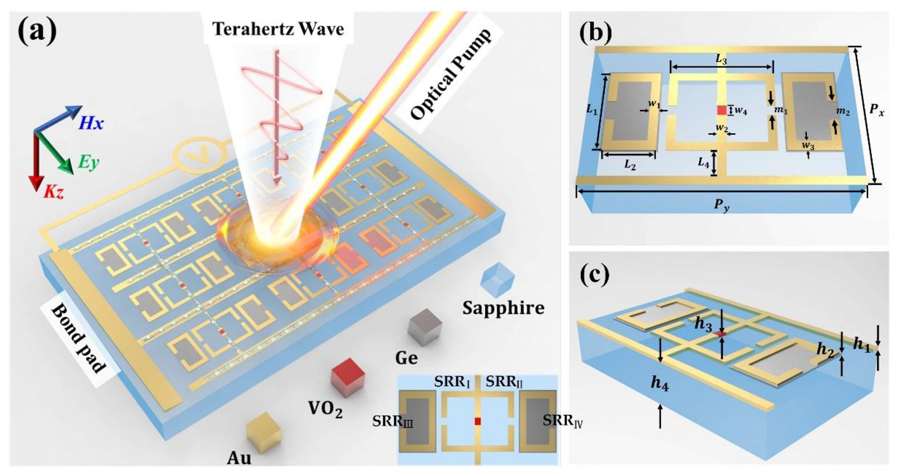
2. Materials and Methods

Figure 1a demonstrates the working principle of the electrically and optically controlled hybrid metasurface that consists of four materials (gold (Au), VO2, Ge, and sapphire). Considering the excellent chemical stability and electrical conductivity, Au was utilized to constitute electrodes and metal parts of resonant units. Four gold split-ring resonators (SRRs) were located symmetrically on the upper surface, with the middle two called SRRI and SRRII and the outer two called SRRIII and SRRIV. In the common long side of SRRI and SRRII, an embedded VO2 bridge was precisely connected to the electrodes and resonators, which could undergo a reversible phase transition triggered by the heat generated from external currents. The dielectric permittivity of VO2 can be described using a Drude model [51]:
ε ω = ε   -   ω p 2 ( σ ) ω 2 + i γ ω
where ε and γ are usually assumed to be 12 and 5.75 × 10¹³ rad/s, plasma frequency ω p 2 ( σ ) is dependent on conductivity, and σ is proportional to the free carrier density [44,52]. Additionally, to properly manipulate resonance intensity, semiconductor layers made of Ge were selected to wrap SRRIII and SRRIV. The entire structure was constructed based on a sapphire substrate with excellent light transmittance. Figure 1b,c illustrate the single unit cell and its geometrical dimensions, while the detail parameters which stem from an overall consideration of the bandwidth, operating frequency, modulation depth, sensitivity, and stability of the device are listed in Table 1. The fabrication process of the device is discussed in S1 (Supplementary Material).
The proposed metasurface’s performance was numerically investigated based on the time-domain solver of the full-wave electromagnetic software CST Microwave Studio 2019. Periodical boundaries were assumed to X and Y directions, and open boundaries were applied in the Z direction. The linear plane waves are normally incident with Y polarization along the negative Z direction. To imitate the phase transition of VO2 induced by electrical voltage, conductivity was varied from 2 × 10² to 2 × 10⁵ S/m [50,52,53]. Similarly, the conductivity of Ge was varied from 1 to 4 × 10³ S/m to simulate the influence of optical pump irradiation [49,54]. It is essential to mention that a 400 nm optical pump (3.1 eV) is typically used to activate the photoinduced carriers in Ge (0.66 eV), and the pump frequency enables the Ge conductivity change to 4 × 10³ S/m that only leads to a slight alteration in undoped VO2 conductivity, thus ensuring independence between the two modulation approaches [52,55,56,57]. The normalized transmission spectra were calculated via the formula: |T(ω)| = |Es(ω)/Er(ω)| with Es(ω) and Er(ω) representing the amplitude of THz waves transmitted through the device and the thickness of bare sapphire, respectively [58].
Figure 2a indicates the behaviors of the current directions and magnetic field (H-field) when VO2 bridges are in the metal phase and Ge layers are unexcited, at which time strong resonances occur at the SRRs. Transmission spectra of the proposed metasurface for two materials with or without excitation are plotted in Figure 2b. To examine the working mechanism of the proposed hybrid metasurface, we separately simulated the two parts of the units, and the surface currents are shown in Figure 2c,e. Considering the nonvolatility of VO2, currents can flow through metal phase VO2 bridges after excitation for a certain period, resulting in opposite current loops on SRRI and SRRII surfaces. Such a current distribution motivates a circular closure of the oscillating H-field that rotates around the two SRRs, which characterizes the appearance of the toroidal dipole and vector T in the space [16]. In the absence of optical pump influence, the conductivity of Ge is approximately equal to 1 S/m, and the current distribution on the surfaces of SRRIII and SRRIV manifests an obvious magnetic dipole type. Figure 2d,f show the simulated transmission spectra for the two different types of resonance modulation. Due to the influence of contrary direction currents flowing on Au electrodes, the resonance intensity of the toroidal dipole is weaker in terms of transmission dip value.

3. Results and Discussions

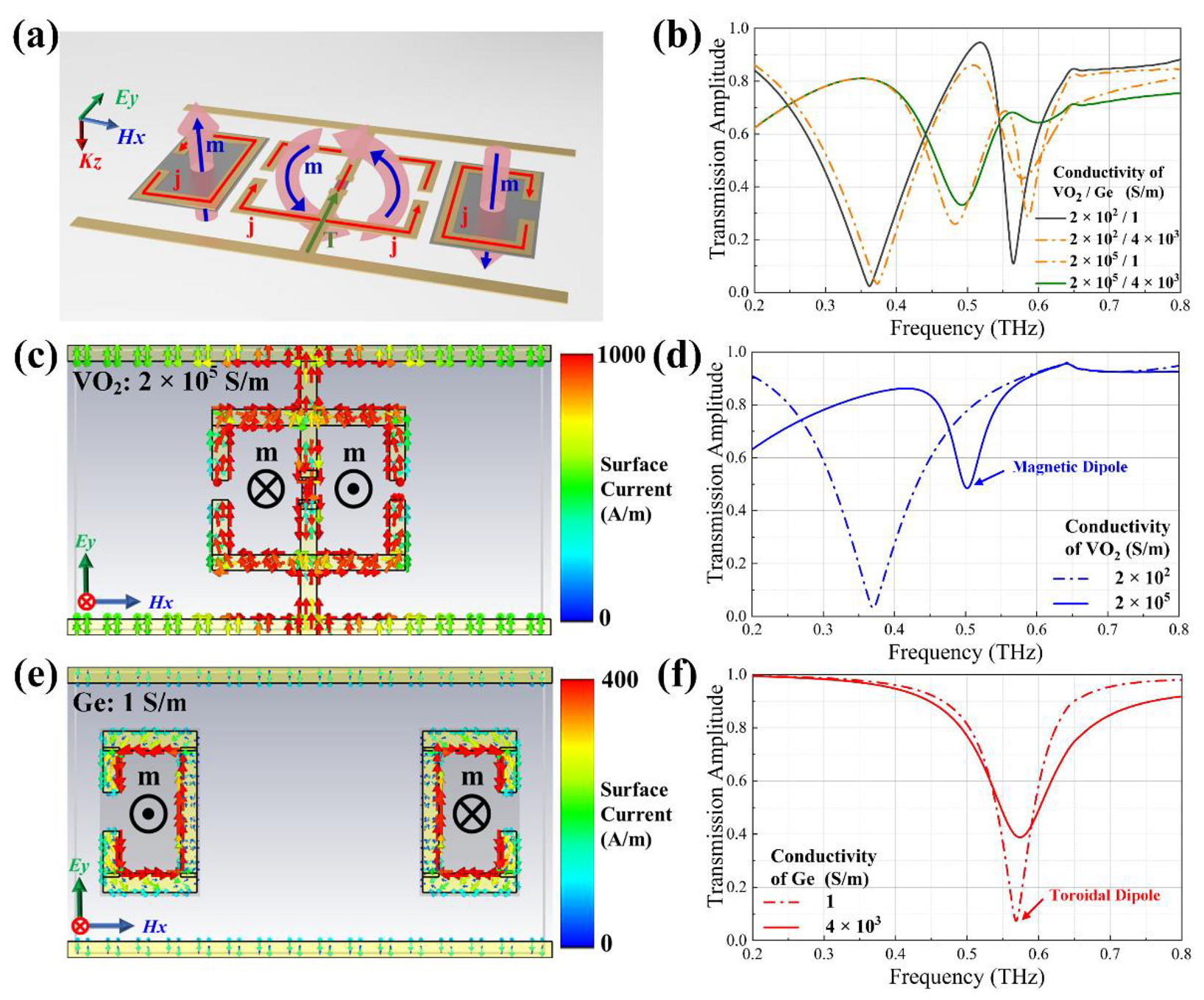
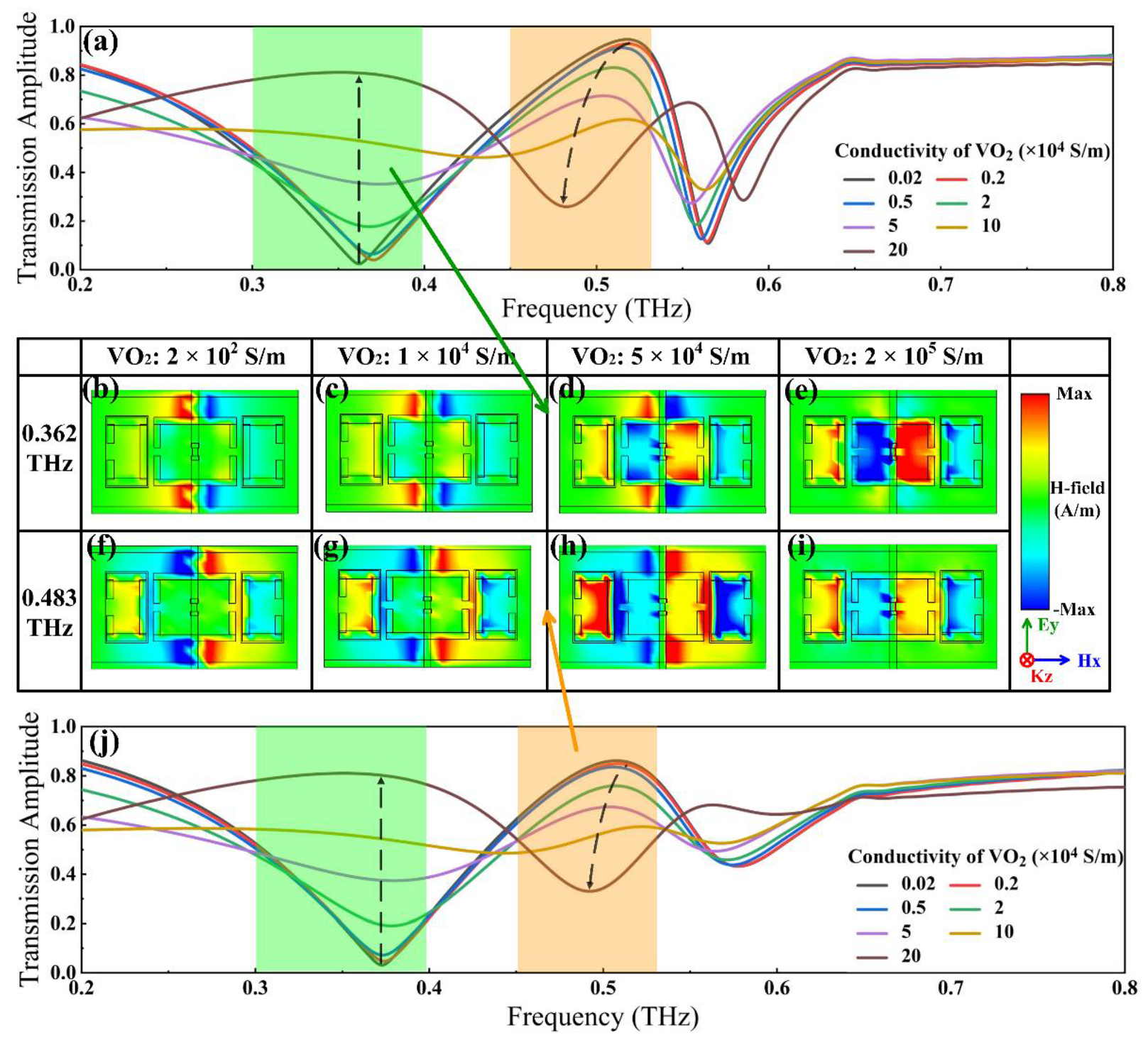
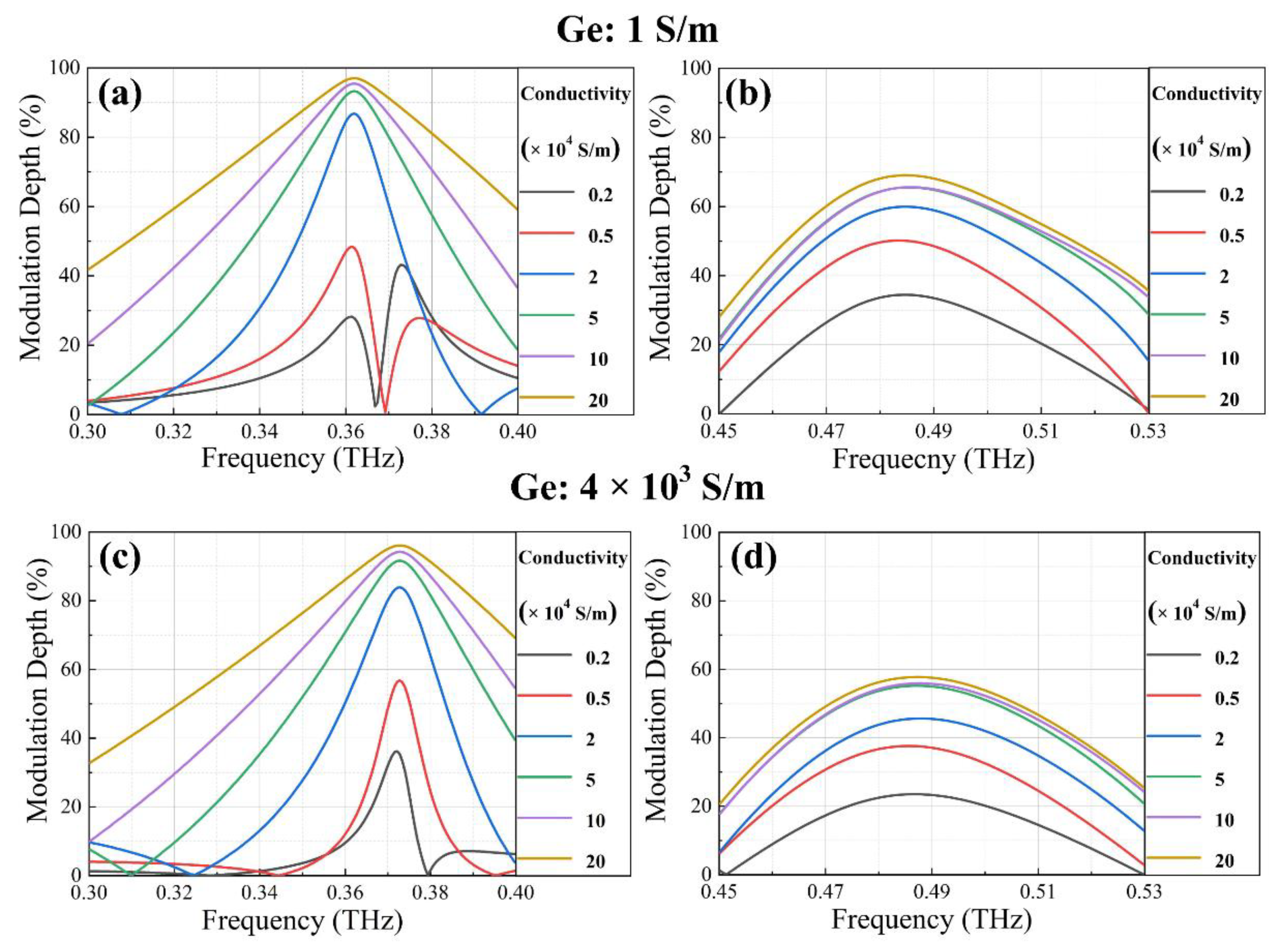
3.1. Simulation of Electrically Tuned VO2 Bridges

We firstly investigated the electrical tuning properties of the hybrid metasurface by simply varying the conductivity of VO2 bridges in the simulation, and the normalized transmission spectra without or with the optical pump irradiation are depicted in Figure 3a,j, respectively. In the absence of external stimuli, Figure 3a presents a transmission dip of 0.02 located at 0.362 THz, accompanied by a peak of 0.95 appearing at 0.518 THz. With the increase in VO2 conductivity, the transmission valley constantly grew while the peak kept dropping. By fixing the VO2 conductivity at 2 × 10⁵ S/m to imitate the ultimate outcome achieved by electrical stimulation, the transmission amplitude at 0.362 THz reached a maximum of 0.81. Meanwhile, a new dip valued at 0.26 occurred at 0.481 THz. Similarly, supposing Ge conductivity of 4 × 10³ S/m, Figure 3j displays transmission amplitudes rising from 0.03 to 0.80 at 0.362 THz, and a peak of 0.86 at 0.508 THz is replaced by the new dip of 0.33 at 0.483 THz alongside the phase transition of VO2. To explain the modifications to transmission spectra, we modeled the alterations to the H-field transmitted through the surface by simply enhancing the VO2 conductivity and fixing the Ge conductivity to 1 S/m at 0.362 THz and 4 × 10³ S/m at 0.483 THz, as shown in Figure 3b–i. As observed, the dip nearby 0.362 THz is caused by the strong resonance on both sides of the gold electrodes, where the H-field gathers when VO2 is in the insulator phase. Increasing the conductivity of VO2 bridges gradually permitted the flux of currents, thus resulting in a toroidal resonance that affected SRRI and SRRII. This was followed by a certain coupling resonance with SRRIII and SRRIV, signified by the transmitted H-field inside. Finally, as VO2 conductivity was set to 2 × 10⁵ S/m, the magnetic field surrounding the electrodes tended to vanish, and a toroidal resonance impacted SRRI and SRRII thereby leading to a transmission dip near 0.483 THz.
To quantitatively analyze the effect of electrical tuning, we adopted modulation depth (MD) to measure the switching ability of the device when dynamically manipulating the transmission of THz waves. For the purpose of precisely unveiling the conversion degree, MD is defined as:
MD = T on   -   T off T on   ×   100 %
where Ton or Toff represents the transmission amplitude when the device is on or off, respectively. By fixing the conductivity of Ge layers at 1 S/m, Figure 4a,b present MD as a function of frequency in the ranges of 0.30–0.40 THz and 0.45–0.53 THz for varying VO2 conductivity. Constant increments in MD with the elevation of VO2 conductivity were perceived, and the maximum MD values of 97.03% and 69.04% eventually appeared at 0.362 THz and 0.485 THz, respectively. With the conductivity of Ge layers set to 4 × 10³ S/m, Figure 4c,d present MD varying with VO2 conductivity in the same frequency ranges, and the maximum MD values of 96.10% and 59.95% appear at 0.372 THz and 0.483 THz, respectively. The frequency shifts of maximum MD are caused by the coupling resonances between SRRs (contributed to by the conductivity of Ge layers), which produces specific influences on the transmission amplitude.

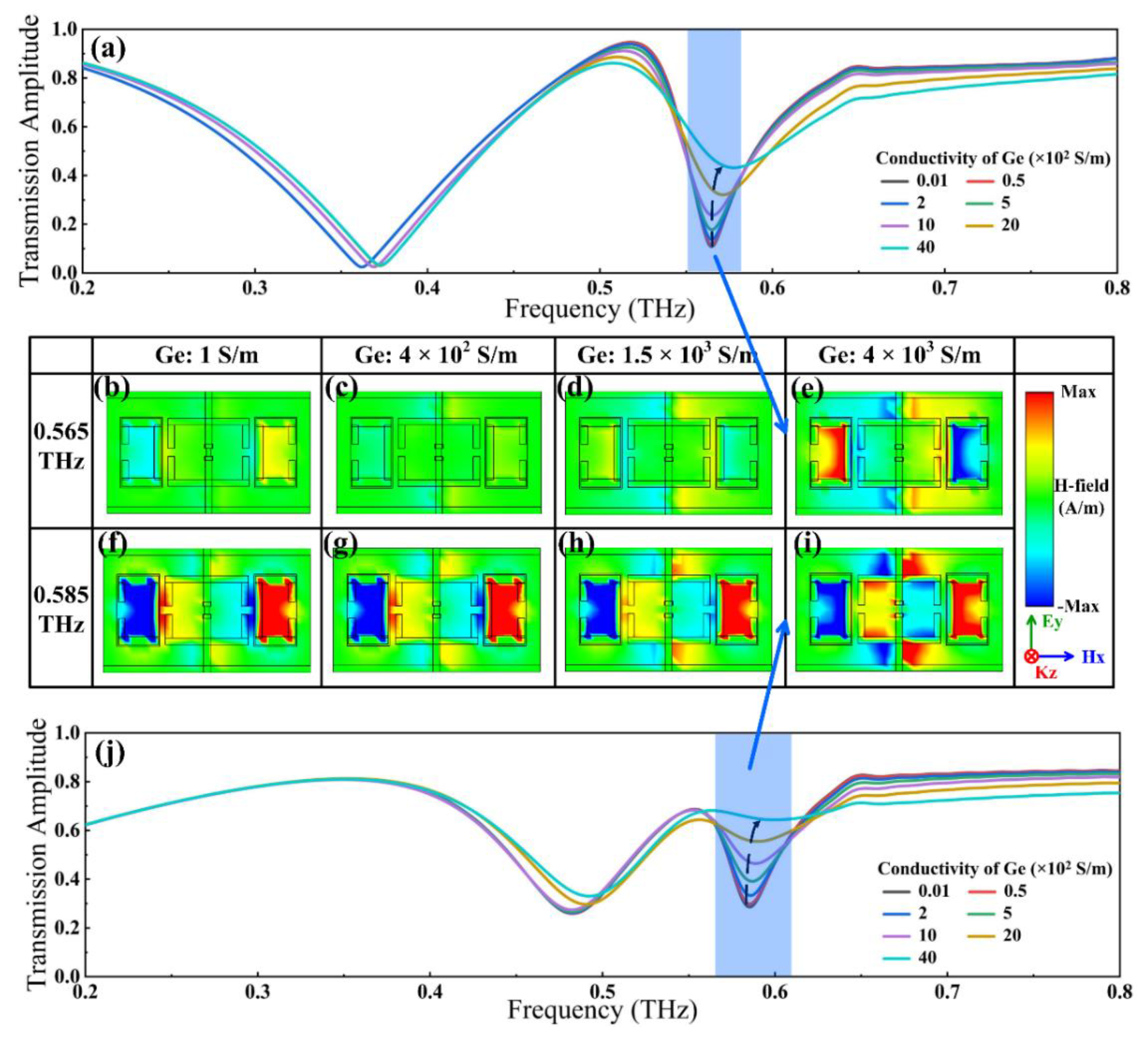
3.2. Simulation of Optically Tuned Ge Layers

The optical tuning properties of the proposed hybrid metasurface were investigated by simply varying the conductivity of Ge layers in the simulation, and the normalized transmission spectra without and with the electrical voltage excitation are depicted in Figure 5a,j. It was noticed that the transmission valley kept elevating with the increase in the conductivity of Ge layers. Independent of external stimuli, a transmission dip of 0.11 emerged at 0.565 THz, which then gradually rose to 0.469 as the conductivity of Ge layers was set to 4 × 10³ S/m. Identically, by fixing VO2 conductivity to 2 × 10⁵ S/m, a transmission dip of 0.285 occurred at 0.585 THz, which finally rose to 0.654 with the enhancement to the conductivity of Ge layers. Supposing VO2 conductivity of 2 × 10² and 2 × 10⁵ S/m, changes in the transmitted H-field with the increase in Ge conductivity at 0.565 and 0.585 THz were observed, as shown in Figure 5b–i. Without optical pumping, the H-field was concentrated inside SRRIII and SRRIV, indicating the predominant position of magnetic dipole resonance in the transmission dip generation. As the Ge layer conductivity elevates, the gradual convergence of the magnetic field toward the electrodes and inside SRRI and SRRII manifests the dropped proportion of the magnetic dipole in the suppressed transmission. Meanwhile, the alternations in the H-field also disclose that other resonance modes are induced due to the interactions with SRRIII, SRRIV, and nearby unit structures. Overall, the resonance strength of the whole unit tends to decline, resulting in improvements in the transmitted H-field and the consequent amelioration of transmission amplitude.
The MD of the metasurface controlled by the optical stimulation was also calculated, as shown in Figure 6a,b. As the conductivity of Ge layers reached 4 × 10³ S/m, the maximum MD reached 77.08% at 0.565 THz and 56.36% at 0.585 THz for two different states of VO2 bridges. The reason for the difference can be interpreted by the changing resonance modes between the gold electrodes and SRRI and SRRII, which in turn leads to disparate coupling strengths with the adjacent SRRIII and SRRIV.

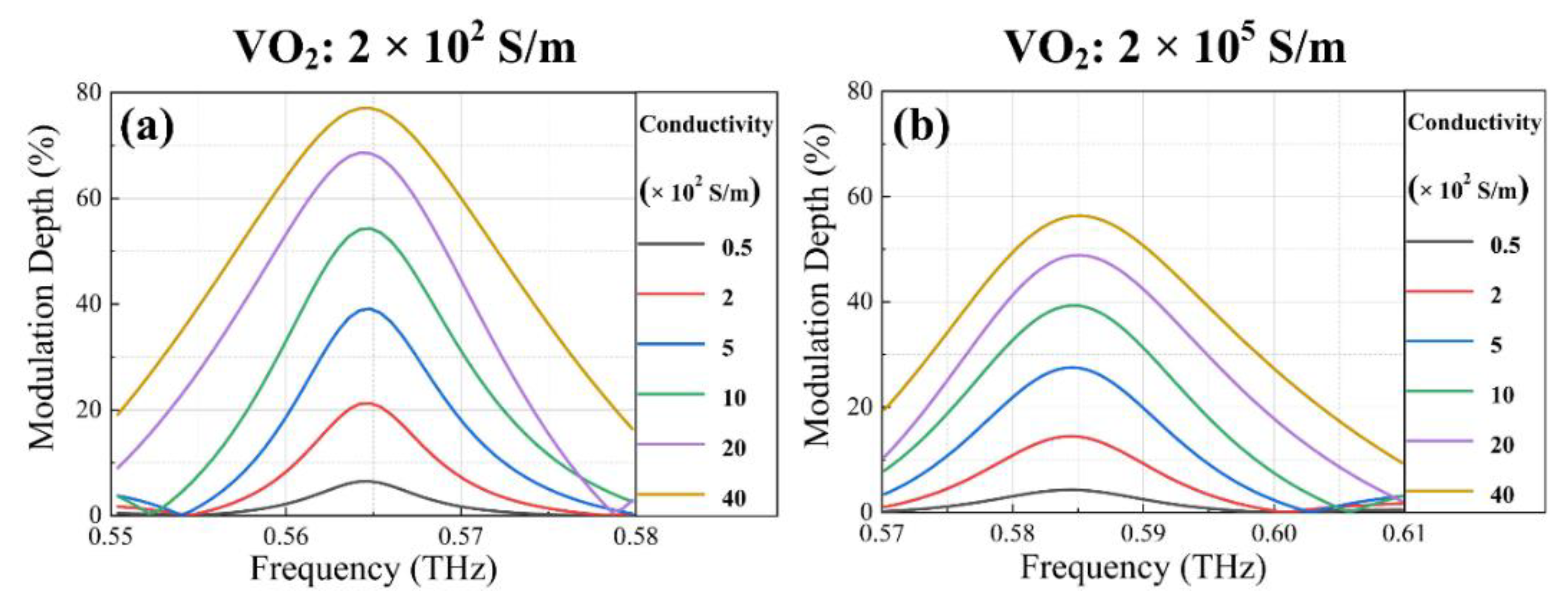
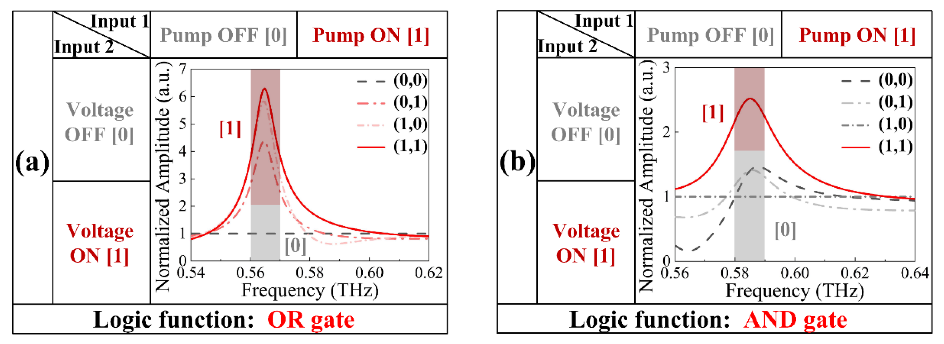
3.3. Logic Operation Controlled by a Multifield

The proposed hybrid metasurface could find wide application. For instance, we further extended our design to realize the logic operation function. Two external input signals were configured as the voltage and optical pump, and the defined “0” and “1” input conditions with or without an external stimulus were respectively imitated by assigning the conductivity of VO2 bridges to 2 × 10² S/m or 2 × 10⁵ S/m and Ge layers to 1 S/m or 4 × 10³ S/m. Notably, the output signals were contingent on weighing the normalized amplitude of transmitted THz waves through standardization of the transmission spectrum of the minimum valley in the frequency range. By exploiting the performance of the device controlled by the electrical and optical methods at 0.56–0.57 THz and 0.58–0.59 THz, the logical operation of two different gates can be independently realized, as depicted in Figure 7.
The data in Figure 7a illustrate the “OR” logic gate executed by the metasurface. Here, the transmission spectrum when applying no external excitation (whereby VO2 conductivity was 2 × 10² S/m and Ge conductivity was 1 S/m) was assumed to have the criterion value of 1. The other normalized amplitudes are observed to be more than four times greater in the range of 0.56–0.57 THz. Therefore, the output of amplitude can be considered as “0” in the absence of stimuli and “1” when modulated by either one or both of the approaches. Figure 7b illustrates the “AND” logic gate in the range of 0.58–0.59 THz, where the transmission spectrum was assumed to be the criterion at the VO2 conductivity of 2 × 10⁵ S/m and the Ge conductivity of 1 S/m. Except for the output tuned by both methods, which was taken as “1” for its amplitude being more than double that of others, the remainders were taken as “0” (for simply one or no stimulus).
From the above analysis, the basic but critical “OR” and “AND” logic operation gates can be implemented, which greatly expands the application of the device. These logic gates are intended not only for simple numerical calculations, but also for functional operations applicable to many scenarios, such as read–erase–write manipulation of information that needs a clear amplitude difference from “1” and “0” output. Considering the “AND” logic gate, the device can output a “1” by individually modulating either VO2 or Ge, thus supplying two degrees of output timing freedom. From the “OR” logic gate, both materials need to be excited together to output a “1”. However, due to the memory property of VO2, it is possible to stimulate Ge at a certain frequency during the phase transition after the excitation of VO2, thereby achieving a continuous ultrafast output of “1”. Therefore, the device we propose possesses some similar functions, such as time-controlled read–erase–write operations. It also has simple time-manipulated information encryption and decryption capabilities when information is being read or written, which undoubtedly enhances the capability of contemporary VO2- or Ge-based information processing.

4. Conclusions

In summary, we have theoretically demonstrated a VO2 and Ge hybrid metasurface that supports electrical and optical control methods individually or simultaneously. To reveal the working mechanism of the designed device, the surface current and transmitted H-field were simulated, which testifies to the dominant role of the toroidal and magnetic dipole resonance strength respectively occupied by the two kinds of material components arranged in the meta-atoms. The switch on-off behaviors and modulation capability at four different frequencies were then investigated. Considering the distinct properties of modulated materials and tuning methods, the four switches possess nonvolatile or temporary on-off speeds to capture two kinds of temporal degrees of freedom. Furthermore, upon active excitation by two stimuli, the device manifests the logical operation functions of “AND” or “OR” gates in two frequency bands, which was confirmed by weighing normalized transmission amplitude. By integrating VO2 and Ge in one device, we have attained a THz metasurface with performance far beyond that of devices equipped with only one single material. Looking forward, such a hybrid metasurface with multiple functions and modulatory degrees of freedom could hold potential for THz photonic and electric meta-device design, which may greatly facilitate applications in data storage, ultrahigh-speed wireless communication, and optic-electric digital processing.

Supplementary Materials

The following supporting information can be downloaded at: https://www.mdpi.com/article/10.3390/nano12213765/s1, S1: Discussion of available fabrication process of the proposed device.

Author Contributions

X.Z. and Y.J. contributed equally to this work. Conceptualization, X.Z., Y.J., J.L. (Jiangang Liang) and T.C.; software, X.Z. and J.L. (Jing Lou); formal analysis, X.Z., Y.J., J.Z., J.L. (Jiawen Lv), X.D., L.S. and B.Z.; writing—original draft preparation, X.Z.; writing—review and editing, J.L. (Jiangang Liang) and T.C. All authors have read and agreed to the published version of the manuscript.

Funding

This work was supported by the National Natural Science Foundation of China (Grant Nos. 61901512, 61905216, 62071423), Natural Science Foundation of Shaanxi Province (2020JM390).

Institutional Review Board Statement

Not applicable.

Informed Consent Statement

Not applicable.

Data Availability Statement

Not applicable.

Conflicts of Interest

The authors declare no conflict of interest.

References

  1. Ma, J.J.; Shrestha, R.; Adelberg, J.; Yeh, C.Y.; Hossain, Z.; Enightly, E.; Jornet, J.M.; Mittleman, D.M. Security and eavesdropping in terahertz wireless links. Nature 2018, 563, 89–93. [Google Scholar] [CrossRef] [PubMed]
  2. Meijer, A.S.; Berden, G.; Arslanov, D.D.; Ozerov, M.; Jongma, R.T.; van der Zande, W.J. An ultrawide-bandwidth single-sideband modulator for terahertz frequencies. Nat. Photonics 2016, 10, 740–744. [Google Scholar] [CrossRef]
  3. Boulogeorgos, A.A.A.; Alexiou, A.; Merkle, T.; Schubert, C.; Elschner, R.; Katsiotis, A.; Stavrianos, P.; Kritharidis, D.; Chartsias, P.K.; Kokkoniemi, J.; et al. Terahertz Technologies to Deliver Optical Network Quality of Experience in Wireless Systems Beyond 5G. IEEE Commun. Mag. 2018, 56, 144–151. [Google Scholar] [CrossRef] [Green Version]
  4. Nagatsuma, T.; Horiguchi, S.; Minamikata, Y.; Yoshimizu, Y.; Hisatake, S.; Kuwano, S.; Yoshimoto, N.; Terada, J.; Takahashi, H. Terahertz wireless communications based on photonics technologies. Opt. Express 2013, 21, 23736–23747. [Google Scholar] [CrossRef] [PubMed] [Green Version]
  5. Seeds, A.J.; Shams, H.; Fice, M.J.; Renaud, C.C. TeraHertz Photonics for Wireless Communications. J. Light. Technol. 2015, 33, 579–587. [Google Scholar] [CrossRef]
  6. Nagatsuma, T.; Ducournau, G.; Renaud, C.C. Advances in terahertz communications accelerated by photonics. Nat. Photonics 2016, 10, 371–379. [Google Scholar] [CrossRef]
  7. Zeng, H.X.; Liang, H.J.; Zhang, Y.X.; Wang, L.; Liang, S.X.; Gong, S.; Li, Z.; Yang, Z.Q.; Zhang, X.L.; Lan, F.; et al. High-precision digital terahertz phase manipulation within a multichannel field perturbation coding chip. Nat. Photonics 2021, 15, 751–757. [Google Scholar] [CrossRef]
  8. Ramachandran, T.; Faruque, M.R.I.; Islam, M.T.; Khandaker, M.U.; Alqahtani, A.; Bradley, D.A. Development and Analysis of Coding and Tailored Metamaterial for Terahertz Frequency Applications. Materials 2022, 15, 2777. [Google Scholar] [CrossRef]
  9. Liu, S.; Cui, T.J.; Zhang, L.; Xu, Q.; Wang, Q.; Wan, X.; Gu, J.Q.; Tang, W.X.; Qi, M.Q.; Han, J.G.; et al. Convolution Operations on Coding Metasurface to Reach Flexible and Continuous Controls of Terahertz. Adv. Sci. 2016, 3, 1600156. [Google Scholar] [CrossRef]
  10. Cai, T.; Tang, S.W.; Bin, Z.; Wang, G.M.; Ji, W.Y.; Qian, C.; Wang, Z.J.; Li, E.P.; Chen, H.S. Ultrawideband chromatic aberration-free meta-mirrors. Adv. Photonics 2021, 3, 16001. [Google Scholar] [CrossRef]
  11. Guo, W.L.; Wang, G.M.; Luo, X.Y.; Chen, K.; Li, H.P.; Feng, Y.J. Dual-Phase Hybrid Metasurface for Independent Amplitude and Phase Control of Circularly Polarized Wave. IEEE Trans. Antennas Propag. 2020, 68, 7705–7710. [Google Scholar] [CrossRef]
  12. Yu, N.F.; Genevet, P.; Kats, M.A.; Aieta, F.; Tetienne, J.P.; Capasso, F.; Gaburro, Z. Light Propagation with Phase Discontinuities: Generalized Laws of Reflection and Refraction. Science 2011, 334, 333–337. [Google Scholar] [CrossRef] [Green Version]
  13. Cai, T.; Zheng, B.; Lou, J.; Shen, L.; Yang, Y.H.; Tang, S.W.; Li, E.; Qian, C.; Chen, H.S. Experimental Realization of a Superdispersion-Enabled Ultrabroadband Terahertz Cloak. Adv. Mater. 2020, 34, 2205053. [Google Scholar] [CrossRef]
  14. Zheludev, N.I.; Kivshar, Y.S. From metamaterials to metadevices. Nat. Mater. 2012, 11, 917–924. [Google Scholar] [CrossRef]
  15. Hu, Y.Z.; You, J.; Tong, M.Y.; Zheng, X.; Xu, Z.J.; Cheng, X.G.; Jiang, T. Pump-Color Selective Control of Ultrafast All-Optical Switching Dynamics in Metaphotonic Devices. Adv. Sci. 2020, 7, 2000799. [Google Scholar] [CrossRef]
  16. Gupta, M.; Srivastava, Y.K.; Singh, R. A Toroidal Metamaterial Switch. Adv. Mater. 2018, 30, 1704845. [Google Scholar] [CrossRef]
  17. Lou, J.; Ma, H.; Wang, J.; Yang, R.S.; Dong, B.W.; Yu, Y.; Wang, J.F.; Zhang, F.L.; Fan, Y.C.; Feng, M.D.; et al. Multifield-Inspired Tunable Carrier Effects Based on Ferroelectric-Silicon PN Heterojunction. Adv. Electron. Mater. 2020, 6, 1900795. [Google Scholar] [CrossRef]
  18. Shen, L.; Lin, X.; Shalaginov, M.Y.; Low, T.; Zhang, X.M.; Zhang, B.L.; Chen, H.S. Broadband enhancement of on-chip single-photon extraction via tilted hyperbolic metamaterials. Appl. Phys. Rev. 2020, 7, 021403. [Google Scholar] [CrossRef]
  19. Chowdhury, D.R.; Singh, R.; O’Hara, J.F.; Chen, H.T.; Taylor, A.J.; Azad, A.K. Dynamically reconfigurable terahertz metamaterial through photo-doped semiconductor. Appl. Phys. Lett. 2011, 99, 231101. [Google Scholar] [CrossRef]
  20. Jeong, Y.G.; Bahk, Y.M.; Kim, D.S. Dynamic Terahertz Plasmonics Enabled by Phase-Change Materials. Adv. Opt. Mater. 2019, 8, 1900548. [Google Scholar] [CrossRef]
  21. Gopalan, P.; Sensale-Rodriguez, B. 2D Materials for Terahertz Modulation. Adv. Opt. Mater. 2019, 8, 1900550. [Google Scholar] [CrossRef]
  22. Hu, T.Z.; Jiang, T.; Zhou, J.H.; Hao, H.; Sun, H.; Ouyang, H.; Tong, M.Y.; Tang, Y.X.; Li, H.; You, J.; et al. Ultrafast terahertz transmission/group delay switching in photoactive WSe2-functionalized metaphotonic devices. Nano Energy 2020, 68, 104280. [Google Scholar] [CrossRef]
  23. Das, S.; Wang, Y.D.; Dai, Y.Y.; Li, S.S.; Sun, Z.P. Ultrafast transient sub-bandgap absorption of monolayer MoS2. Light Sci. Appl. 2021, 10, 27. [Google Scholar] [CrossRef]
  24. Lee, K.; Li, J.; Cheng, L.; Wang, J.; Kumar, D.; Wang, Q.S.; Chen, M.J.; Wu, Y.; Eda, G.; Chia, E.E.M.; et al. Sub-Picosecond Carrier Dynamics Induced by Efficient Charge Transfer in MoTe2/WTe2 van der Waals Heterostructures. ACS Nano 2019, 13, 9587–9594. [Google Scholar] [CrossRef] [PubMed]
  25. Chanana, A.; Liu, X.J.; Zhang, C.; Vardeny, Z.V.; Nahata, A. Ultrafast frequency-agile terahertz devices using methylammonium lead halide perovskites. Sci. Adv. 2018, 4, eaar7353. [Google Scholar] [CrossRef] [PubMed] [Green Version]
  26. Zhong, Y.C.; Tang, B.; Fei, M.; Jie, Q.; Tan, J.Q.; Wang, Q.Q.; Liang, S.; Du, J.J.; Zhang, L.; Dong, H.X.; et al. All-Photonic Miniature Perovskite Encoder with a Terahertz Bandwidth. Laser Photonics Rev. 2020, 14, 1900398. [Google Scholar] [CrossRef]
  27. Li, Z.Q.; Liu, X.Y.; Zuo, C.L.; Yang, W.; Fang, X.S. Supersaturation-Controlled Growth of Monolithically Integrated Lead-Free Halide Perovskite Single-Crystalline Thin Film for High-Sensitivity Photodetectors. Adv. Mater. 2021, 33, 2103010. [Google Scholar] [CrossRef]
  28. Dai, Z.J.; Manjappa, M.; Yang, Y.K.; Tan, T.C.W.; Qiang, B.; Han, S.; Wong, L.J.; Xiu, F.X.; Liu, W.W.; Singh, R. High Mobility 3D Dirac Semimetal (Cd3As2) for Ultrafast Photoactive Terahertz Photonics. Adv. Funct. Mater. 2021, 31, 2011011. [Google Scholar] [CrossRef]
  29. Ding, F. A Review of Multifunction Optical Gap-Surface Plasmon Metasurfaces. Prog. Electromagn. Res. 2020, 174, 55–73. [Google Scholar] [CrossRef]
  30. Goulain, P.; Koulouklidis, A.D.; Manceau, J.M.; Daskalaki, C.; Paulillo, B.; Maussang, K.; Dhillon, S.; Freeman, J.R.; Li, L.H.; Linfield, E.H.; et al. Femtosecond Broadband Frequency Switch of Terahertz Three-Dimensional Meta-Atoms. ACS Photonics 2021, 8, 1097–1102. [Google Scholar] [CrossRef]
  31. Lou, J.; Liang, J.G.; Yu, Y.; Ma, H.; Yang, R.S.; Fan, Y.C.; Wang, G.M.; Cai, T. Silicon-Based Terahertz Meta-Devices for Electrical Modulation of Fano Resonance and Transmission Amplitude. Adv. Opt. Mater. 2020, 8, 2000449. [Google Scholar] [CrossRef]
  32. Meng, C.; Thrane, P.C.V.; Bozhevolnyi, S.I. Full-range birefringence control with piezoelectric MEMS-based metasurfaces. Nat. Commun. 2020, 13, 2071. [Google Scholar] [CrossRef]
  33. Zhang, J.; Hu, X.F.; Chen, H.S.; Gao, F. Designer Surface Plasmons Enable Terahertz Cherenkov Radiation. Prog. Electromagn. Res. 2020, 169, 25–32. [Google Scholar] [CrossRef]
  34. Liu, X.D.; Chen, H.; Liang, S.X.; Zhang, M.; Jiang, Z.D.; Fan, S.T.; Sun, Y.W. Ultrabroadband electrically controllable terahertz modulation based on GaAs Schottky diode structure. APL Photonics 2021, 6, 111301. [Google Scholar] [CrossRef]
  35. Liu, X.B.; Wang, Q.; Zhang, X.Q.; Li, H.; Xu, Q.; Xu, Y.H.; Chen, X.Y.; Li, S.X.; Liu, M.; Tian, Z.; et al. Thermally Dependent Dynamic Meta-Holography Using a Vanadium Dioxide Integrated Metasurface. Adv. Opt. Mater. 2019, 7, 1900175. [Google Scholar] [CrossRef]
  36. Lee, S.; Kim, W.T.; Kang, J.H.; Kang, B.J.; Rotermund, F.; Park, Q.H. Single-Layer Metasurfaces as Spectrally Tunable Terahertz Half- and Quarter-Waveplates. ACS Appl. Mater. Interfaces 2019, 11, 7655–7660. [Google Scholar] [CrossRef]
  37. Zhang, M.; Ma, X.L.; Pu, M.B.; Liu, K.P.; Guo, Y.H.; Huang, Y.J.; Xie, X.; Li, X.; Yu, H.L.; Luo, X.G. Large-Area and Low-Cost Nanoslit-Based Flexible Metasurfaces for Multispectral Electromagnetic Wave Manipulation. Adv. Opt. Mater. 2019, 7, 1900657. [Google Scholar] [CrossRef]
  38. Fan, X.Q.; Li, Y.H.; Chen, S.H.; Xing, Y.F.; Pan, T.S. Mechanical Terahertz Modulation by Skin-Like Ultrathin Stretchable Metasurface. Small 2020, 16, 2002484. [Google Scholar] [CrossRef]
  39. Degl’Innocenti, R.; Kindness, S.J.; Beere, H.E.; Ritchie, D.A. All-integrated terahertz modulators. Nanophotonics 2018, 7, 127–144. [Google Scholar] [CrossRef]
  40. Shrekenhamer, D.; Chen, W.C.; Padilla, W.J. Liquid Crystal Tunable Metamaterial Absorber. Phys. Rev. Lett. 2013, 110, 177403. [Google Scholar] [CrossRef]
  41. Kowerdziej, P.; Stanczyk, T.; Parka, J. Electromagnetic simulations of tunable terahertz metamaterial infiltrated with highly birefringent nematic liquid crystal. Liq. Cryst. 2015, 42, 430–434. [Google Scholar] [CrossRef]
  42. Chen, X.Y.; Zhang, S.J.; Liu, K.; Li, H.Y.; Xu, Y.H.; Chen, J.J.; Lu, Y.C.; Wang, Q.W.; Feng, X.; Wang, K.M.; et al. Reconfigurable and Nonvolatile Terahertz Metadevices Based on a Phase-Change Material. ACS Photonics 2022, 9, 1638–1646. [Google Scholar] [CrossRef]
  43. Wang, Y.F.; Landreman, P.; Schoen, D.; Okabe, K.; Marshall, A.; Celano, U.; Wong, H.S.P.; Park, J.; Brongersma, M.L. Electrical tuning of phase-change antennas and metasurfaces. Nat. Nanotechnol. 2021, 16, 667–672. [Google Scholar] [CrossRef] [PubMed]
  44. Song, Z.Y.; Chen, A.P.; Zhang, J.H. Terahertz switching between broadband absorption and narrowband absorption. Opt. Express 2020, 28, 2037–2044. [Google Scholar] [CrossRef] [PubMed]
  45. Liu, M.K.; Hwang, H.Y.; Tao, H.; Strikwerda, A.C.; Fan, K.B.; Keiser, G.R.; Sternbach, A.J.; West, K.G.; Kittiwatanakul, S.; Lu, J.W.; et al. Terahertz-field-induced insulator-to-metal transition in vanadium dioxide metamaterial. Nature 2012, 487, 345–348. [Google Scholar] [CrossRef]
  46. Kabir, S.; Nirantar, S.; Zhu, L.C.; Ton-That, C.; Jain, S.K.; Kayani, A.B.; Murdoch, B.J.; Sriram, S.; Walia, S.; Bhaskaran, M. Phase change vanadium dioxide light sensors. Appl. Mater. Today 2020, 21, 100833. [Google Scholar] [CrossRef]
  47. Ding, F.; Zhong, S.M.; Bozhevolnyi, S.I. Vanadium Dioxide Integrated Metasurfaces with Switchable Functionalities at Terahertz Frequencies. Adv. Opt. Mater. 2018, 6, 1701204. [Google Scholar] [CrossRef]
  48. Li, X.K.; Tang, S.W.; Ding, F.; Zhong, S.M.; Yang, Y.Q.; Jiang, T.; Zhou, J. Switchable multifunctional terahertz metasurfaces employing vanadium dioxide. Sci. Rep. 2019, 9, 5454. [Google Scholar] [CrossRef] [Green Version]
  49. Hu, Y.Z.; Tong, M.Y.; Xu, Z.J.; Cheng, X.G.; Jiang, T. Spatiotemporal Terahertz Metasurfaces for Ultrafast All-Optical Switching with Electric-Triggered Bistability. Laser Photonics Rev. 2021, 15, 2000456. [Google Scholar] [CrossRef]
  50. Lu, C.; Lu, Q.J.; Gao, M.; Lin, Y. Dynamic Manipulation of THz Waves Enabled by Phase-Transition VO2 Thin Film. Nanomaterrials 2021, 11, 114. [Google Scholar] [CrossRef]
  51. Ulbricht, R.; Hendry, E.; Shan, J.; Heinz, T.F.; Bonn, M. Carrier dynamics in semiconductors studied with time-resolved terahertz spectroscopy. Rev. Mod. Phys. 2011, 83, 543. [Google Scholar] [CrossRef] [Green Version]
  52. Zhao, X.L.; Lou, J.; Xu, X.; Wang, G.M.; Qi, J.H.; Zeng, L.X.; He, J.; Liang, J.G.; Huang, Y.D.; Zhang, D.P.; et al. Multifield Controlled Terahertz Modulator Based on Silicon-Vanadium Dioxide Hybrid Metasurface. Adv. Opt. Mater. 2022, 10, 2102589. [Google Scholar] [CrossRef]
  53. Wang, L.; Hong, W.J.; Deng, L.; Li, S.F.; Zhang, C.; Zhu, J.F.; Wang, H.J. Reconfigurable Multifunctional Metasurface Hybridized with Vanadium Dioxide at Terahertz Frequencies. Materials 2018, 11, 2040. [Google Scholar] [CrossRef] [Green Version]
  54. Lim, W.X.; Manjappa, M.; Srivastava, Y.K.; Cong, L.Q.; Kumar, A.; MacDonald, K.F.; Singh, R. Ultrafast All-Optical Switching of Germanium-Based Flexible Metaphotonic Devices. Adv. Mater. 2018, 30, 1705331. [Google Scholar] [CrossRef] [Green Version]
  55. Lou, J.; Xu, X.; Huang, Y.D.; Yu, Y.; Wang, J.; Fang, G.Y.; Liang, J.G.; Fan, C.H.; Chang, C. Optically Controlled Ultrafast Terahertz Metadevices with Ultralow Pump Threshold. Small 2021, 17, 2104275. [Google Scholar] [CrossRef]
  56. Liu, H.; Lysenko, S.; Rua, A.; Vikhnin, V.; Zhang, G.; Vasquez, O.; Fernandez, F.E. Laser excitation and excited state dynamics in vanadium dioxide thin film. J. Lumin. 2006, 119, 404–411. [Google Scholar] [CrossRef]
  57. Hsieh, W.P.; Trigo, M.; Reis, D.A.; Artioli, G.A.; Malavasi, L.; Mao, W.L. Evidence for photo-induced monoclinic metallic VO2 under high pressure. Appl. Phys. Lett. 2014, 104, 21917. [Google Scholar] [CrossRef]
  58. Lou, J.; Yang, R.S.; Liang, J.G.; Yu, Y.; Zhang, L.; Zhang, C.B.; Li, T.J.; Fan, Y.C.; Zhang, F.L.; Wang, G.M.; et al. Dual-Sensitivity Terahertz Metasensor Based on Lattice–Toroidal-Coupled Resonance. Adv. Photonics Res. 2020, 2, 2000175. [Google Scholar] [CrossRef]
Figure 1. Schematics and working principle of the proposed hybrid metasurface. (a) Schematic illustration of the metasurface; the phase change material VO2 and the semiconductor material Ge are controlled by external voltage and the optical pump, respectively. (b,c) The detailed parameters of the unit cell.
Nanomaterials 12 03765 g001
Figure 2. Resonance schematics and simulated transmission spectra of the designed unit. (a) Diagram of the transmit directions of the magnetic field and surface current. (b) Transmission spectra of the proposed metasurface for both materials with or without excitation. (c) Surface current distribution on SRRI and SRRII alone at the VO2 conductivity of 2 × 10⁵ S/m. (d) Transmission spectra of SRRI and SRRII alone for VO2 with or without excitation. (e) Surface current distribution on SRRIII and SRRIV alone at the Ge conductivity of 4 × 10³ S/m. (f) Transmission spectra of SRRIII and SRRIV alone for Ge with or without excitation.
Nanomaterials 12 03765 g002
Figure 3. Characterizations of the hybrid metasurface modulated by the electrical method. Transmission spectra depending VO2 bridge conductivity when the conductivity of the Ge layer was fixed at (a) 1 S/m and (j) 4 × 10³ S/m. (be) Distributions of the H-field transmitted through the surface with the increase in VO2 bridge conductivity at 0.362 THz when fixing Ge layers at 1 S/m. (fi) Distributions of the H-field transmitted through the surface with the increase in VO2 bridge conductivity at 0.362 THz when fixing Ge layers at 4 × 10³ S/m.
Nanomaterials 12 03765 g003
Figure 4. MD for varying VO2 conductivity with and without optical pump irradiation. (a,b) MD depending on the conductivity of VO2 bridges at 0.30–0.40 THz and 0.45–0.53 THz when the conductivity of Ge layers is 1 S/m. (c,d) MD depending on the conductivity of VO2 bridges at 0.30–0.40 THz and 0.45–0.53 THz when the conductivity of Ge layers is 4 × 10³ S/m.
Nanomaterials 12 03765 g004
Figure 5. Characterizations of the hybrid metasurface modulated by the optical method. (a,j) Transmission spectra depending on Ge layer conductivity when conductivity of VO2 bridges is fixed at (a) 2 × 10² S/m and (j) 2 × 10⁵ S/m. (be) Distributions of the H-field transmitted through the surface with the increase in Ge layer conductivity at 0.565 THz when fixing VO2 bridges at 2 × 10² S/m. (fi) Distributions of the H-field transmitted through the surface with the increase in Ge layer conductivity at 0.585 THz when fixing VO2 bridges at 2 × 10⁵ S/m.
Nanomaterials 12 03765 g005
Figure 6. MD for varying Ge conductivity without and with the electrical voltage excitation. (a) MD depending on the conductivity of Ge layers at 0.55–0.58 THz when the conductivity of VO2 bridges is 2 × 10² S/m. (b) MD depending on the conductivity of Ge layers at 0.57–0.61 THz when the conductivity of VO2 bridges is 2 × 10⁵ S/m.
Nanomaterials 12 03765 g006
Figure 7. The dual-stimulus-controlled hybrid metasurface is functionalized as a logic (a) OR gate at 0.56–0.57 THz and (b) AND gate at 0.58–0.59 THz.
Nanomaterials 12 03765 g007
Table 1. Parameter configuration of the proposed THz hybrid metasurface (μm).
PxPyL1L2L3L4w1w2
150905029601555
w3w4m1m2h1h2h3h4
666120.50.30.55 × 105
Publisher’s Note: MDPI stays neutral with regard to jurisdictional claims in published maps and institutional affiliations.

