
Anisotropic Radiation in Heterostructured “Emitter in a Cavity” Nanowire

 , , , , and
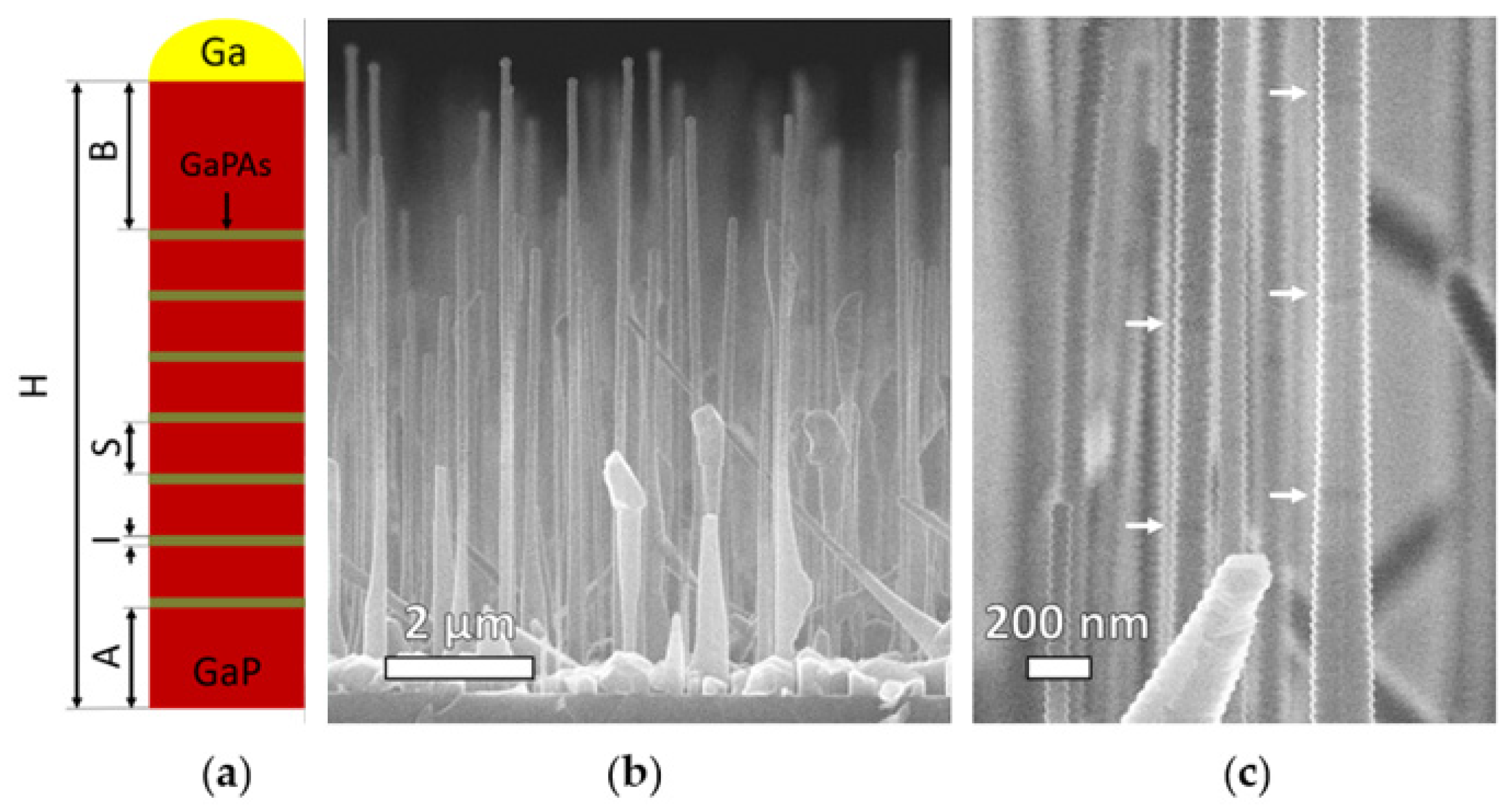
Abstract
:1. Introduction
2. Materials and Methods
2.1. Nanowire Synthesis
2.2. Microscopy and Spectroscopy
2.3. Modeling
3. Results
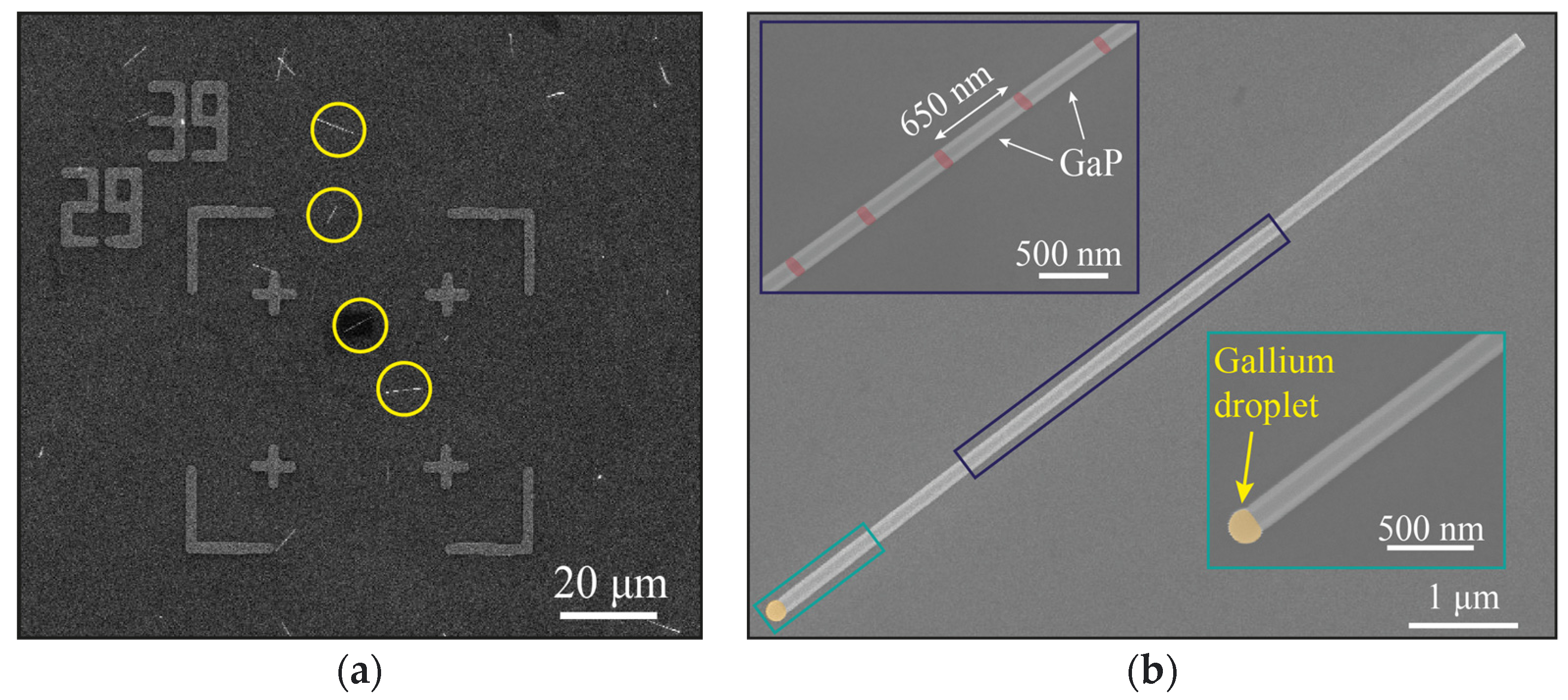
3.1. NW Morphology Study and Preparation for PL Characterization
3.2. Micro-PL Study
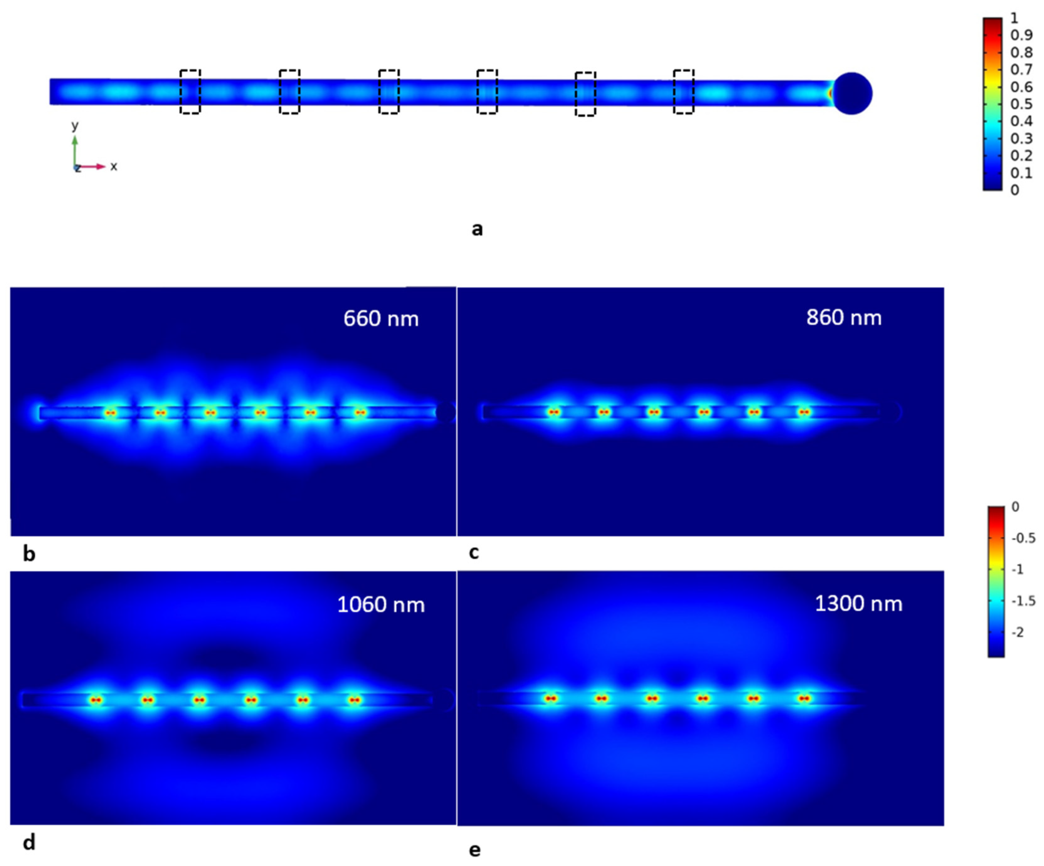
3.3. Modeling Results
4. Discussion
- -
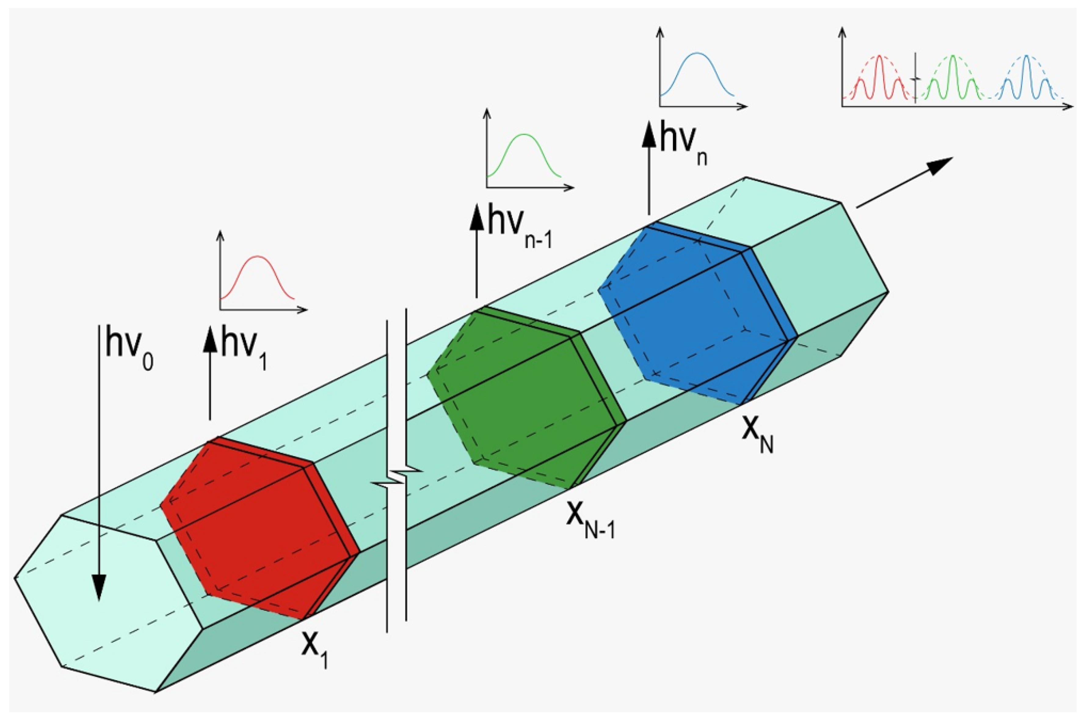
- The emission of an individual ND is anisotropic and is coupled inside the NW, while part of it is emitted outside the NW;
- -
- The emission outside the NW in the vicinity of an ND is due to the PL of the ND and not due to the scattering of the light propagating in the cavity, so this emission should be governed by the bandgap of the ND and can be controlled via the variation of its chemical composition;
- -
- The non-uniform distribution of the excitation light along the NW governed by the wavelength and NW geometry affects the PL intensity of each emitter;
- -
- Outcoupling is the most efficient at the NW edge without the catalyst droplet;
- -
- The emission outcoupled at the NW edge is modulated due to the NW geometry promoting its resonant optical properties.
5. Conclusions
Author Contributions
Funding
Institutional Review Board Statement
Informed Consent Statement
Data Availability Statement
Acknowledgments
Conflicts of Interest
References
- Shen, Y.; Harris, N.C.; Skirlo, S.; Prabhu, M.; Baehr-Jones, T.; Hochberg, M.; Sun, X.; Zhao, S.; Larochelle, H.; Englund, D.; et al. Deep learning with coherent nanophotonic circuits. Nat. Photonics 2017, 11, 441–446. [Google Scholar] [CrossRef]
- Wei, H.; Xu, H. Nanowire-based plasmonic waveguides and devices for integrated nanophotonic circuits. Nanophotonics 2012, 1, 155–169. [Google Scholar] [CrossRef]
- Ledentsov, N.N. Quantum dot laser. Semicond. Sci. Technol. 2011, 26, 014001. [Google Scholar] [CrossRef]
- Zhukov, A.E.; Kovsh, A.R.; Ustinov, V.M.; Shernyakov, Y.M.; Mikhrin, S.S.; Maleev, N.A.; Kondrat’eva, E.Y.; Livshits, D.A.; Maximov, M.V.; Volovik, B.V.; et al. Continuous-wave operation of long-wavelength quantum-dot diode laser on a GaAs substrate. IEEE Photonics Technol. Lett. 1999, 11, 1345–1347. [Google Scholar] [CrossRef]
- Bimberg, D.; Grundmann, M.; Heinrichsdorff, F.; Ledentsov, N.N.; Ustinov, V.M.; Zhukov, A.E.; Kovsh, A.R.; Maximov, M.V.; Shernyakov, Y.M.; Volovik, B.V.; et al. Quantum dot lasers: Breakthrough in optoelectronics. Thin Solid Films 2000, 367, 235–249. [Google Scholar] [CrossRef]
- Krogstrup, P.; Jørgensen, H.I.; Heiss, M.; Demichel, O.; Holm, J.V.; Aagesen, M.; Nygard, J.; Fontcuberta I Morral, A. Single-nanowire solar cells beyond the Shockley-Queisser limit. Nat. Photonics 2013, 7, 306–309. [Google Scholar] [CrossRef] [Green Version]
- Wu, Z.H.; Mei, X.Y.; Kim, D.; Blumin, M.; Ruda, H.E. Growth of Au-catalyzed ordered GaAs nanowire arrays by molecular-beam epitaxy. Appl. Phys. Lett. 2002, 81, 5177–5179. [Google Scholar] [CrossRef]
- Kuykendall, T.; Pauzauskie, P.; Lee, S.; Zhang, Y.; Goldberger, J.; Yang, P. Metalorganic chemical vapor deposition route to GaN nanowires with triangular cross sections. Nano Lett. 2003, 3, 1063–1066. [Google Scholar] [CrossRef]
- Wang, J.; Gao, L. Hydrothermal synthesis and photoluminescence properties of zno nanowires. Solid State Commun. 2004, 132, 269–271. [Google Scholar] [CrossRef]
- Plissard, S.; Dick, K.A.; Larrieu, G.; Godey, S.; Addad, A.; Wallart, X.; Caroff, P. Gold-free growth of GaAs nanowires on silicon: Arrays and polytypism. Nanotechnology 2010, 21, 385602. [Google Scholar] [CrossRef]
- Fontcuberta I Morral, A.; Spirkoska, D.; Arbiol, J.; Heigoldt, M.; Morante, J.R.; Abstreiter, G. Prismatic quantum heterostructures synthesized on molecular-beam epitaxy GaAs nanowires. Small 2008, 4, 899–903. [Google Scholar] [CrossRef] [PubMed] [Green Version]
- Trofimov, P.; Pushkarev, A.P.; Sinev, I.S.; Fedorov, V.V.; Bruyère, S.; Bolshakov, A.; Mukhin, I.S.; Makarov, S.V. Perovskite-Gallium Phosphide Platform for Reconfigurable Visible-Light Nanophotonic Chip. ACS Nano 2020, 14, 8126–8134. [Google Scholar] [CrossRef] [PubMed]
- Lu, W.; Xie, P.; Lieber, C.M. Nanowire transistor performance limits and applications. IEEE Trans. Electron Devices 2008, 55, 2859–2876. [Google Scholar] [CrossRef]
- Zhou, W.; Dai, X.; Fu, T.M.; Xie, C.; Liu, J.; Lieber, C.M. Long term stability of nanowire nanoelectronics in physiological environments. Nano Lett. 2014, 14, 1614–1619. [Google Scholar] [CrossRef] [PubMed] [Green Version]
- Bolshakov, A.D.; Fedorov, V.V.; Shugurov, K.Y.; Mozharov, A.M.; Sapunov, G.A.; Shtrom, I.V.; Mukhin, M.S.; Uvarov, A.V.; Cirlin, G.E.; Mukhin, I.S. Effects of the surface preparation and buffer layer on the morphology, electronic and optical properties of the GaN nanowires on Si. Nanotechnology 2019, 30, 395602. [Google Scholar] [CrossRef]
- Patolsky, F.; Timko, B.P.; Zheng, G.; Lieber, C.M. Nanowire-based nanoelectronic devices in the life sciences. MRS Bull. 2007, 32, 142–149. [Google Scholar] [CrossRef] [Green Version]
- Ramgir, N.S.; Yang, Y.; Zacharias, M. Nanowire-based sensors. Small 2010, 6, 1705–1722. [Google Scholar] [CrossRef]
- Kretinin, A.V.; Popovitz-Biro, R.; Mahalu, D.; Shtrikman, H. Multimode Fabry-Pérot conductance oscillations in suspended stacking-faults-free InAs nanowires. Nano Lett. 2010, 10, 3439–3455. [Google Scholar] [CrossRef]
- Duan, X.; Huang, Y.; Agarwal, R.; Lieber, C.M. Single-nanowire elecctrically driven lasers. Nature 2003, 421, 241–245. [Google Scholar] [CrossRef]
- Tchernycheva, M.; Messanvi, A.; De Luna Bugallo, A.; Jacopin, G.; Lavenus, P.; Rigutti, L.; Zhang, H.; Halioua, Y.; Julien, F.H.; Eymery, J.; et al. Integrated photonic platform based on InGaN/GaN nanowire emitters and detectors. Nano Lett. 2014, 14, 3515–3520. [Google Scholar] [CrossRef]
- Tateno, K.; Zhang, G.; Gotoh, H.; Sogawa, T. VLS growth of alternating InAsP/InP heterostructure nanowires for multiple-quantum-dot structures. Nano Lett. 2012, 12, 2888–2893. [Google Scholar] [CrossRef] [PubMed]
- Lauhon, L.J.; Gudlksen, M.S.; Wang, D.; Lieber, C.M. Epitaxial core-shell and core-multishell nanowire heterostructures. Nature 2002, 420, 57–61. [Google Scholar] [CrossRef]
- Minot, E.D.; Kelkensberg, F.; Van Kouwen, M.; Van Dam, J.A.; Kouwenhoven, L.P.; Zwiller, V.; Borgström, M.T.; Wunnicke, O.; Verheijen, M.A.; Bakkers, E.P.A.M. Single quantum dot nanowire LEDs. Nano Lett. 2007, 7, 367–371. [Google Scholar] [CrossRef] [PubMed] [Green Version]
- Qian, F.; Li, Y.; Gradečak, S.; Park, H.G.; Dong, Y.; Ding, Y.; Wang, Z.L.; Lieber, C.M. Multi-quantum-well nanowire heterostructures for wavelength-controlled lasers. Nat. Mater. 2008, 7, 701–706. [Google Scholar] [CrossRef]
- Leandro, L.; Gunnarsson, C.P.; Reznik, R.; Jöns, K.D.; Shtrom, I.; Khrebtov, A.; Kasama, T.; Zwiller, V.; Cirlin, G.; Akopian, N. Nanowire Quantum Dots Tuned to Atomic Resonances. Nano Lett. 2018, 18, 7217–7221. [Google Scholar] [CrossRef] [Green Version]
- Claudon, J.; Bleuse, J.; Malik, N.S.; Bazin, M.; Jaffrennou, P.; Gregersen, N.; Sauvan, C.; Lalanne, P.; Gérard, J.-M. A highly efficient single-photon source based on a quantum dot in a photonic nanowire. Nat. Photonics 2010, 4, 174–177. [Google Scholar] [CrossRef]
- Holmes, M.J.; Choi, K.; Kako, S.; Arita, M.; Arakawa, Y. Room-temperature triggered single photon emission from a III-nitride site-controlled nanowire quantum dot. Nano Lett. 2014, 14, 982–986. [Google Scholar] [CrossRef]
- Huber, T.; Predojević, A.; Khoshnegar, M.; Dalacu, D.; Poole, P.J.; Majedi, H.; Weihs, G. Polarization entangled photons from quantum dots embedded in nanowires. Nano Lett. 2014, 14, 7107–7114. [Google Scholar] [CrossRef] [Green Version]
- Versteegh, M.A.M.; Reimer, M.E.; Jöns, K.D.; Dalacu, D.; Poole, P.J.; Gulinatti, A.; Giudice, A.; Zwiller, V. Observation of strongly entangled photon pairs from a nanowire quantum dot. Nat. Commun. 2014, 5, 5298. [Google Scholar] [CrossRef]
- Tatebayashi, J.; Ota, Y.; Ishida, S.; Nishioka, M.; Iwamoto, S.; Arakawa, Y. Highly uniform, multi-stacked InGaAs/GaAs quantum dots embedded in a GaAs nanowire. Appl. Phys. Lett. 2014, 105, 103104. [Google Scholar] [CrossRef]
- Verardo, D.; Lindberg, F.W.; Anttu, N.; Niman, C.S.; Lard, M.; Dabkowska, A.P.; Nylander, T.; Månsson, A.; Prinz, C.N.; Linke, H. Nanowires for Biosensing: Lightguiding of Fluorescence as a Function of Diameter and Wavelength. Nano Lett. 2018, 18, 4796–4802. [Google Scholar] [CrossRef]
- Fedorov, V.V.; Bolshakov, A.; Sergaeva, O.; Neplokh, V.; Markina, D.; Bruyere, S.; Saerens, G.; Petrov, M.I.; Grange, R.; Timofeeva, M.; et al. Gallium Phosphide Nanowires in a Free-Standing, Flexible, and Semitransparent Membrane for Large-Scale Infrared-to-Visible Light Conversion. ACS Nano 2020, 14, 10624–10632. [Google Scholar] [CrossRef]
- Haffouz, S.; Zeuner, K.D.; Dalacu, D.; Poole, P.J.; Lapointe, J.; Poitras, D.; Mnaymneh, K.; Wu, X.; Couillard, M.; Korkusinski, M.; et al. Bright Single InAsP Quantum Dots at Telecom Wavelengths in Position-Controlled InP Nanowires: The Role of the Photonic Waveguide. Nano Lett. 2018, 18, 3047–3052. [Google Scholar] [CrossRef] [Green Version]
- Tatebayashi, J.; Kako, S.; Ho, J.; Ota, Y.; Iwamoto, S.; Arakawa, Y. Room-temperature lasing in a single nanowire with quantum dots. Nat. Photonics 2015, 9, 501–505. [Google Scholar] [CrossRef]
- Yang, L.; Motohisa, J.; Fukui, T.; Jia, L.X.; Zhang, L.; Geng, M.M.; Chen, P.; Liu, Y.L.; Wang, T. Fabry-Pérot microcavity modes observed in the micro-photoluminescence spectra of the single nanowire with InGaAs/GaAs heterostructure. Opt. Express 2009, 17, 9337–9346. [Google Scholar] [CrossRef]
- Frolov, A.Y.; Verellen, N.; Li, J.; Zheng, X.; Paddubrouskaya, H.; Denkova, D.; Shcherbakov, M.R.; Vandenbosch, G.A.E.; Panov, V.I.; Van Dorpe, P.; et al. Near-Field Mapping of Optical Fabry-Perot Modes in All-Dielectric Nanoantennas. Nano Lett. 2017, 17, 7629–7637. [Google Scholar] [CrossRef] [PubMed]
- Wiecha, P.R.; Cuche, A.; Arbouet, A.; Girard, C.; Colas Des Francs, G.; Lecestre, A.; Larrieu, G.; Fournel, F.; Larrey, V.; Baron, T.; et al. Strongly Directional Scattering from Dielectric Nanowires. ACS Photonics 2017, 4, 2036–2046. [Google Scholar] [CrossRef] [Green Version]
- Abujetas, D.R.; Paniagua-Domínguez, R.; Sánchez-Gil, J.A. Unraveling the Janus Role of Mie Resonances and Leaky/Guided Modes in Semiconductor Nanowire Absorption for Enhanced Light Harvesting. ACS Photonics 2015, 2, 921–929. [Google Scholar] [CrossRef] [Green Version]
- Mohtashami, Y.; DeCrescent, R.A.; Heki, L.K.; Iyer, P.P.; Butakov, N.A.; Wong, M.S.; Alhassan, A.; Mitchell, W.J.; Nakamura, S.; DenBaars, S.P.; et al. Light-emitting metalenses and meta-axicons for focusing and beaming of spontaneous emission. Nat. Commun. 2021, 12, 3591. [Google Scholar] [CrossRef] [PubMed]
- Anttu, N. Modifying the emission of light from a semiconductor nanowire array. J. Appl. Phys. 2016, 120, 043108. [Google Scholar] [CrossRef]
- Chesin, J.; Gradecak, S. Comparing directed efficiency of III-nitride nanowire light-emitting diodes. J. Nanophotonics 2014, 8, 083095. [Google Scholar] [CrossRef]
- Paniagua-Domínguez, R.; Grzela, G.; Rivas, J.G.; Sánchez-Gil, J.A. Enhanced and directional emission of semiconductor nanowires tailored through leaky/guided modes. Nanoscale 2013, 5, 10582–10590. [Google Scholar] [CrossRef] [PubMed] [Green Version]
- Roy, P.; Bolshakov, A.D. Ga-GaP nanowire hybrid optical system for enhanced coupling, focusing and steering of light. J. Phys. D Appl. Phys. 2020, 53, 295101. [Google Scholar] [CrossRef]
- Ishizaka, A.; Shiraki, Y. Low Temperature Surface Cleaning of Silicon and Its Application to Silicon MBE. J. Electrochem. Soc. 1986, 133, 666. [Google Scholar] [CrossRef]
- Okumura, H.; Akane, T.; Tsubo, Y.; Matsumoto, S. Comparison of Conventional Surface Cleaning Methods for Si Molecular Beam Epitaxy. J. Electrochem. Soc. 1997, 144, 3765. [Google Scholar] [CrossRef]
- Fedorov, V.V.; Berdnikov, Y.; Sibirev, N.V.; Bolshakov, A.D.; Fedina, S.V.; Sapunov, G.A.; Dvoretckaia, L.N.; Cirlin, G.; Kirilenko, D.A.; Tchernycheva, M.; et al. Tailoring morphology and vertical yield of self-catalyzed gap nanowires on template-free si substrates. Nanomaterials 2021, 11, 1949. [Google Scholar] [CrossRef]
- Bolshakov, A.D.; Fedorov, V.V.; Sibirev, N.V.; Fetisova, M.V.; Moiseev, E.I.; Kryzhanovskaya, N.V.; Koval, O.Y.; Ubyivovk, E.V.; Mozharov, A.M.; Cirlin, G.E.; et al. Growth and Characterization of GaP/GaPAs Nanowire Heterostructures with Controllable Composition. Phys. Status Solidi-Rapid Res. Lett. 2019, 13, 1900350. [Google Scholar] [CrossRef]
- Sharov, V.A.; Bolshakov, A.D.; Fedorov, V.V.; Bruyere, S.; Cirlin, G.E.; Alekseev, P.A.; Mukhin, I.S. Deep-Subwavelength Raman Imaging of the Strained GaP Nanowires. J. Phys. Chem. C 2020, 124, 14054–14060. [Google Scholar] [CrossRef]
- Rubenstein, M. The Preparation of Homogeneous and Reproducible Solid Solutions of GaP-GaAs. J. Electrochem. Soc. 1965, 112, 426. [Google Scholar] [CrossRef]
- Hua, B.; Motohisa, J.; Ding, Y.; Hara, S.; Fukui, T. Characterization of Fabry-Pérot microcavity modes in GaAs nanowires fabricated by selective-area metal organic vapor phase epitaxy. Appl. Phys. Lett. 2007, 91, 131112. [Google Scholar] [CrossRef] [Green Version]
- Dobrovolsky, A.; Stehr, J.E.; Sukrittanon, S.; Kuang, Y.; Tu, C.W.; Chen, W.M.; Buyanova, I.A. Fabry-Perot Microcavity Modes in Single GaP/GaNP Core/Shell Nanowires. Small 2015, 11, 6331–6337. [Google Scholar] [CrossRef]
- Khmelevskaia, D.; Markina, D.I.; Fedorov, V.V.; Ermolaev, G.A.; Arsenin, A.V.; Volkov, V.S.; Goltaev, A.S.; Zadiranov, Y.M.; Tzibizov, I.A.; Pushkarev, A.P.; et al. Directly grown crystalline gallium phosphide on sapphire for nonlinear all-dielectric nanophotonics. Appl. Phys. Lett. 2021, 118, 201101. [Google Scholar] [CrossRef]
- Poddubny, A.N.; Ginzburg, P.; Belov, P.A.; Zayats, A.V.; Kivshar, Y.S. Tailoring and enhancing spontaneous two-photon emission using resonant plasmonic nanostructures. Phys. Rev. A-At. Mol. Opt. Phys. 2012, 86, 033826. [Google Scholar] [CrossRef] [Green Version]
- Ginzburg, P.; Zayats, A.V. Localized surface plasmon resonances in spatially dispersive nano-objects: Phenomenological treatise. ACS Nano 2013, 7, 4334–4342. [Google Scholar] [CrossRef] [PubMed]


Publisher’s Note: MDPI stays neutral with regard to jurisdictional claims in published maps and institutional affiliations. |
© 2022 by the authors. Licensee MDPI, Basel, Switzerland. This article is an open access article distributed under the terms and conditions of the Creative Commons Attribution (CC BY) license (https://creativecommons.org/licenses/by/4.0/).
Share and Cite
Kuznetsov, A.; Roy, P.; Kondratev, V.M.; Fedorov, V.V.; Kotlyar, K.P.; Reznik, R.R.; Vorobyev, A.A.; Mukhin, I.S.; Cirlin, G.E.; Bolshakov, A.D. Anisotropic Radiation in Heterostructured “Emitter in a Cavity” Nanowire. Nanomaterials 2022, 12, 241. https://doi.org/10.3390/nano12020241
Kuznetsov A, Roy P, Kondratev VM, Fedorov VV, Kotlyar KP, Reznik RR, Vorobyev AA, Mukhin IS, Cirlin GE, Bolshakov AD. Anisotropic Radiation in Heterostructured “Emitter in a Cavity” Nanowire. Nanomaterials. 2022; 12(2):241. https://doi.org/10.3390/nano12020241
Chicago/Turabian StyleKuznetsov, Alexey, Prithu Roy, Valeriy M. Kondratev, Vladimir V. Fedorov, Konstantin P. Kotlyar, Rodion R. Reznik, Alexander A. Vorobyev, Ivan S. Mukhin, George E. Cirlin, and Alexey D. Bolshakov. 2022. "Anisotropic Radiation in Heterostructured “Emitter in a Cavity” Nanowire" Nanomaterials 12, no. 2: 241. https://doi.org/10.3390/nano12020241
APA StyleKuznetsov, A., Roy, P., Kondratev, V. M., Fedorov, V. V., Kotlyar, K. P., Reznik, R. R., Vorobyev, A. A., Mukhin, I. S., Cirlin, G. E., & Bolshakov, A. D. (2022). Anisotropic Radiation in Heterostructured “Emitter in a Cavity” Nanowire. Nanomaterials, 12(2), 241. https://doi.org/10.3390/nano12020241