
Ordered Bose Glass of Vortices in Superconducting YBa2Cu3O7−δ Thin Films with a Periodic Pin Lattice Created by Focused Helium Ion Irradiation
 , , and
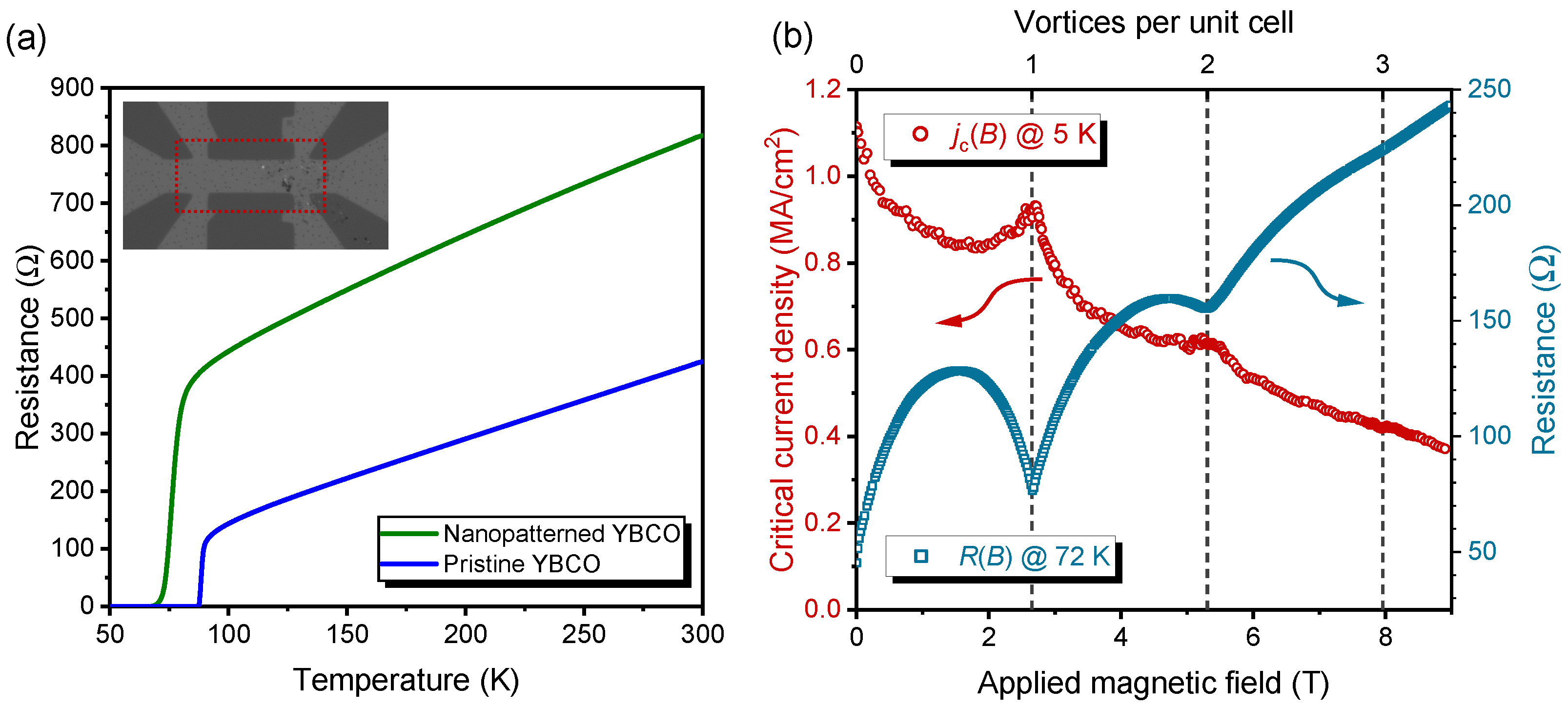
Abstract
1. Introduction
2. Theoretical Background
3. Materials and Methods
3.1. Sample Preparation
3.2. Focused Ion-Beam Irradiation
3.3. Electrical Measurements
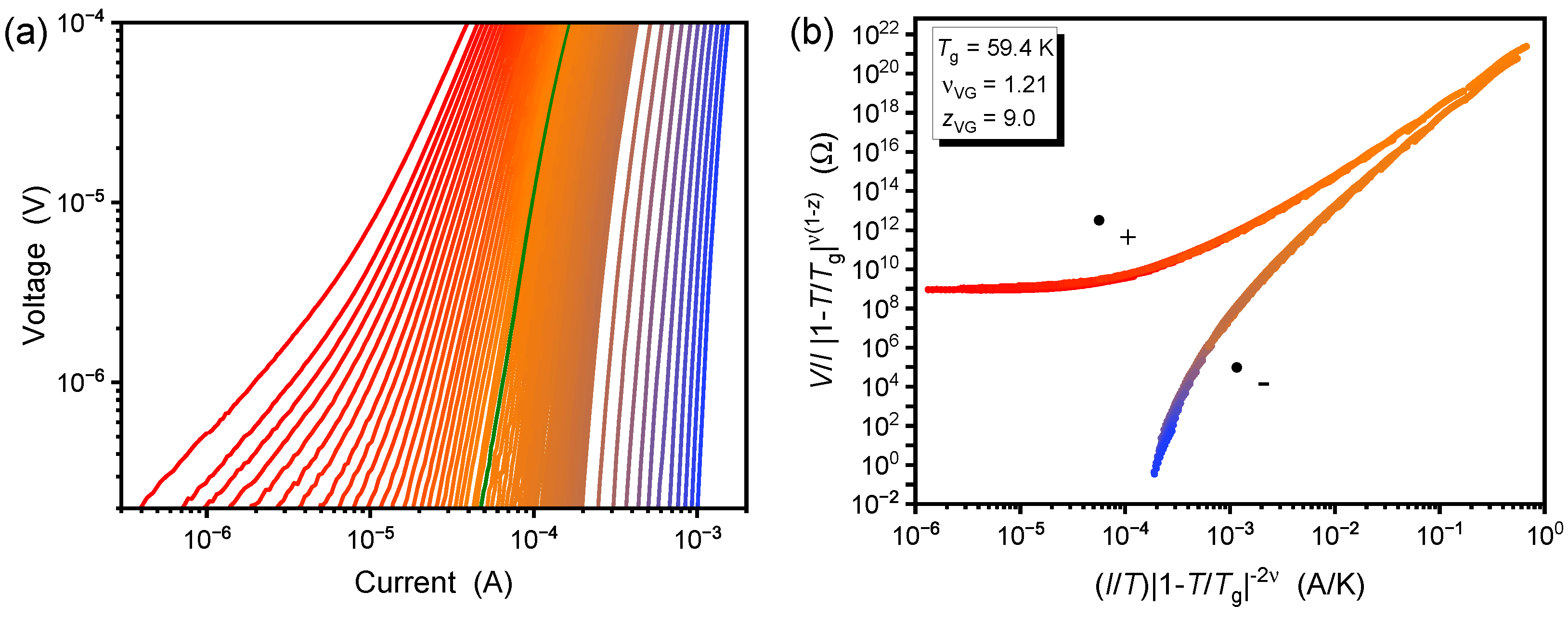
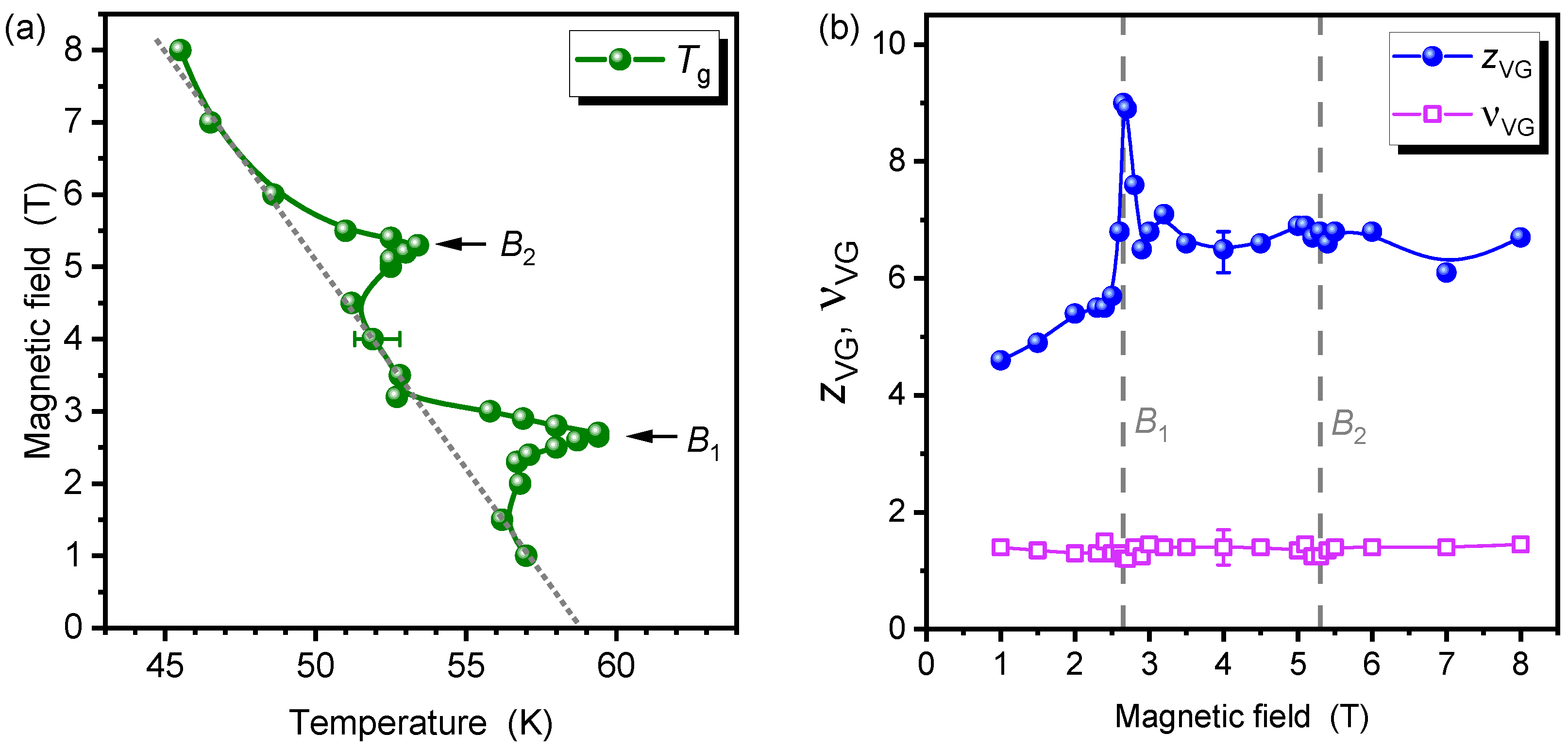
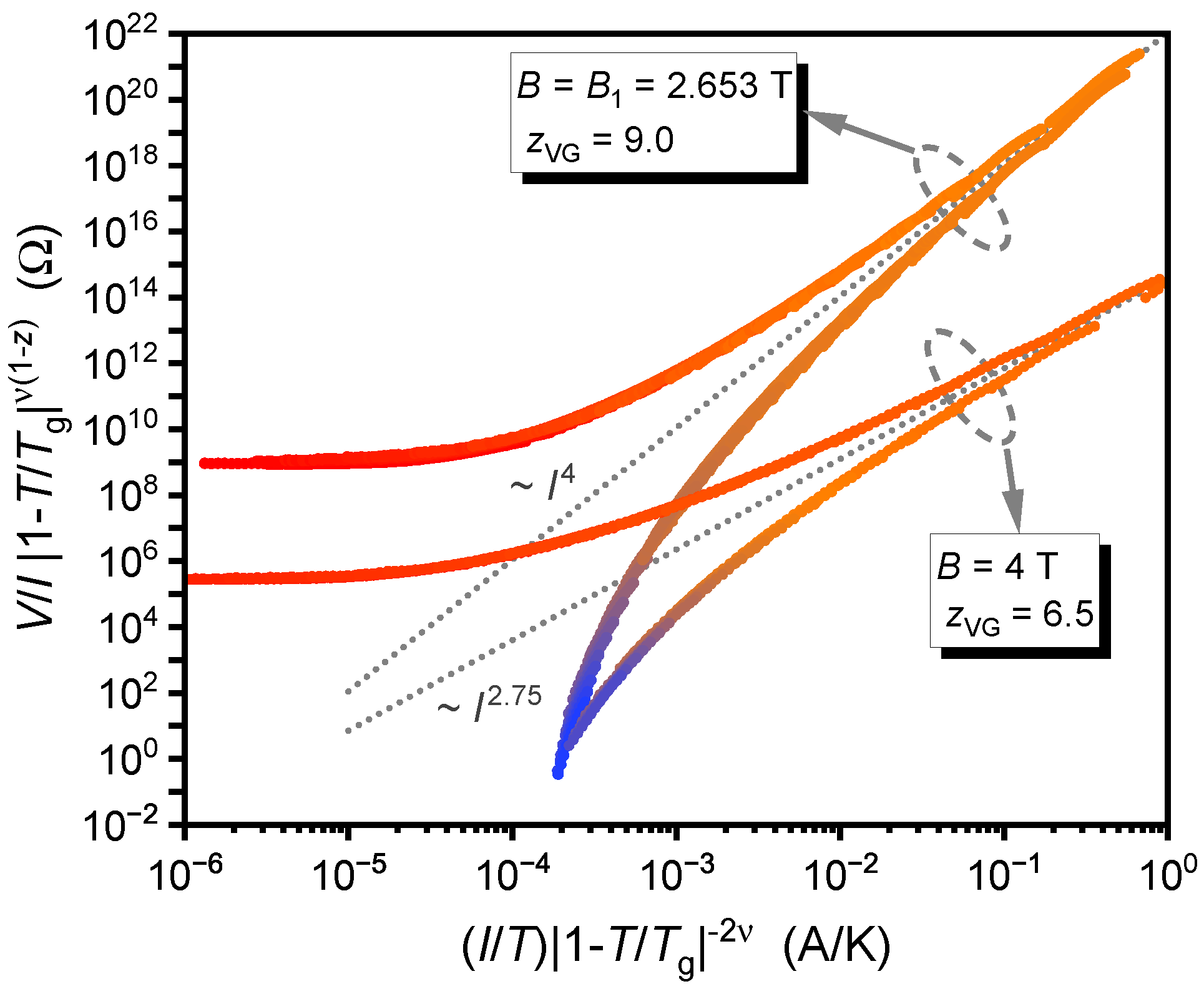
4. Results and Discussion
5. Conclusions
Author Contributions
Funding
Data Availability Statement
Conflicts of Interest
References
- Blatter, G.; Feigel’man, M.V.; Geshkenbein, V.B.; Larkin, A.I.; Vinokur, V.M. Vortices in high-temperature superconductors. Rev. Mod. Phys. 1994, 66, 1125–1388. [Google Scholar] [CrossRef]
- Wördenweber, R.; Moshchalkov, V.; Bending, S.; Tafuri, F. (Eds.) Superconductors at the Nanoscale: From Basic Research to Applications; de Gruyter: Berlin, Germany, 2017. [Google Scholar] [CrossRef]
- Vallès, F.; Palau, A.; Abraimov, D.; Jaroszynski, J.; Constantinescu, A.M.; Mundet, B.; Obradors, X.; Larbalestier, D.; Puig, T. Optimizing vortex pinning in YBa2Cu3O7−x superconducting films up to high magnetic fields. Commun. Mater. 2022, 3, 45. [Google Scholar] [CrossRef]
- Anderson, P.W. Theory of Flux Creep in Hard Superconductors. Phys. Rev. Lett. 1962, 9, 309–311. [Google Scholar] [CrossRef]
- Kim, Y.B.; Hempstead, C.F.; Strnad, A.R. Critical Persistent Currents in Hard Superconductors. Phys. Rev. Lett. 1962, 9, 306–309. [Google Scholar] [CrossRef]
- Kes, P.H.; Aarts, J.; van den Berg, J.; van der Beek, J.C.; Mydosh, J.A. Thermally Assisted Flux Flow at Small Driving Forces. Supercond. Sci. Technol. 1989, 1, 242–248. [Google Scholar] [CrossRef]
- Reichhardt, C.; Olson Reichhardt, C.J. Depinning and nonequilibrium dynamic phases of particle assemblies driven over random and ordered substrates: A review. Rep. Prog. Phys. 2017, 80, 026501. [Google Scholar] [CrossRef]
- Fisher, M. Vortex Glass Superconductivity: A Possible New Phase in Bulk High-Tc Oxides. Phys. Rev. Lett. 1989, 62, 1415. [Google Scholar] [CrossRef] [PubMed]
- Fisher, D.S.; Fisher, M.P.A.; Huse, D.A. Thermal Fluctuations, Quenched Disorder, Phase Transitions, and Transport in Type-II Superconductors. Phys. Rev. 1991, 43, 130–159. [Google Scholar] [CrossRef] [PubMed]
- Nelson, D.R.; Vinokur, V.M. Boson Localization and Pinning by Correlated Disorder in High-Temperature Superconductors. Phys. Rev. Lett. 1992, 68, 2398–2401. [Google Scholar] [CrossRef]
- Nelson, D.R.; Vinokur, V.M. Boson Localization and Correlated Pinning of Superconducting Vortex Arrays. Phys. Rev. B 1993, 48, 13060–13097. [Google Scholar] [CrossRef]
- Koch, R.; Foglietti, V.; Gallagher, W.; Koren, G.; Gupta, A.; Fisher, M. Experimental Evidence for Vortex-Glass Superconductivity in Y-Ba-Cu-O. Phys. Rev. Lett. 1989, 63, 1511. [Google Scholar] [CrossRef] [PubMed]
- Hou, L.F.; Deak, J.; Metcalf, P.; Mcelfresh, M. Effect of Oxygen Stoichiometry on the Vortex-Glass Phase Transition in YBa2Cu3O7−δ Thin Films. Phys. Rev. B 1994, 50, 7226–7229. [Google Scholar] [CrossRef] [PubMed]
- Dekker, C.; Wöltgens, P.J.M.; Koch, R.H.; Hussey, B.W.; Gupta, A. Absence of a finite-temperature vortex-glass phase transition in two-dimensional YBa2Cu3O7−δ films. Phys. Rev. Lett. 1992, 69, 2717–2720. [Google Scholar] [CrossRef] [PubMed]
- Gammel, P.L.; Schneemeyer, L.F.; Bishop, D.J. SQUID Picovoltometry of YBa2Cu3O7 Single Crystals: Evidence for a Finite-Temperature Phase Transition in the High-Field Vortex State. Phys. Rev. Lett. 1991, 66, 953–956. [Google Scholar] [CrossRef]
- Safar, H.; Gammel, P.L.; Bishop, D.J.; Mitzi, D.B.; Kapitulnik, A. SQUID Picovoltometry of Single Crystal Bi2Sr2CaCu2O8+δ: Observation of the Crossover from High-Temperature Arrhenius to Low-Temperature Vortex-Glass Behavior. Phys. Rev. Lett. 1992, 68, 2672–2675. [Google Scholar] [CrossRef]
- Yamasaki, H.; Endo, K.; Kosaka, S.; Umeda, M.; Yoshida, S.; Kajimura, K. Quasi-two-dimensional vortex-glass transition observed in epitaxial Bi2Sr2CaCu2Ox thin films. Phys. Rev. B 1994, 50, 12959–12965. [Google Scholar] [CrossRef]
- Sefrioui, Z.; Arias, D.; Varela, M.; Villegas, J.E.; de la Torre, M.A.L.; León, C.; Loos, G.D.; Santamaría, J. Crossover from a three-dimensional to purely two-dimensional vortex-glass transition in deoxygenated YBa2Cu3O7−δ thin films. Phys. Rev. B 1999, 60, 15423–15429. [Google Scholar] [CrossRef]
- Lang, W.; Fussenegger, C.; Proyer, S.; Stangl, E.; Bäuerle, D. Observation of the vortex-glass transition in YBa2Cu3O7 by phase-resolved current-voltage measurements. Z. Phys. B 1996, 100, 13–18. [Google Scholar] [CrossRef]
- Krusin-Elbaum, L.; Civale, L.; Blatter, G.; Marwick, A.D.; Holtzberg, F.; Feild, C. Bose-glass melting in YBaCuO crystals with correlated disorder. Phys. Rev. Lett. 1994, 72, 1914–1917. [Google Scholar] [CrossRef]
- Wöltgens, P.J.M.; Dekker, C.; Swüste, J.; de Wijn, H.W. Superconducting Phase of YBa2Cu3O7−δ Films in High Magnetic Fields: Vortex Glass or Bose Glass. Phys. Rev. B 1993, 48, 16826–16829. [Google Scholar] [CrossRef]
- Safar, H.; Foltyn, S.R.; Jia, Q.X.; Maley, M.P. Bose glass vortex phase transition in twinned YBa2Cu3O7−δ superconductors. Philos. Mag. B 1996, 74, 647–654. [Google Scholar] [CrossRef]
- Horide, T.; Matsumoto, K.; Mele, P.; Ichinose, A.; Kita, R.; Mukaida, M.; Yoshida, Y.; Horii, S. The crossover from the vortex glass to the Bose glass in nanostructured YBa2Cu3O7−x films. Appl. Phys. Lett. 2008, 92, 182511. [Google Scholar] [CrossRef]
- Lang, W.; Dineva, M.; Marksteiner, M.; Enzenhofer, T.; Siraj, K.; Peruzzi, M.; Pedarnig, J.D.; Bäuerle, D.; Korntner, R.; Cekan, E.; et al. Ion-beam direct-structuring of high-temperature superconductors. Microelectron. Eng. 2006, 83, 1495–1498. [Google Scholar] [CrossRef]
- Lang, W.; Richter, H.; Marksteiner, M.; Siraj, K.; Bodea, M.A.; Pedarnig, J.D.; Grigoropoulos, C.; Bäuerle, D.; Hasenfuss, C.; Palmetshofer, L.; et al. Masked ion beam irradiation of high-temperature superconductors: Patterning of nano-size regions with high point-defect density. Int. J. Nanotechnol. 2009, 6, 704–714. [Google Scholar] [CrossRef]
- Pedarnig, J.D.; Siraj, K.; Bodea, M.A.; Puica, I.; Lang, W.; Kolarova, R.; Bauer, P.; Haselgrübler, K.; Hasenfuss, C.; Beinik, I.; et al. Surface planarization and masked ion-beam structuring of YBa2Cu3O7 thin films. Thin Solid Film. 2010, 518, 7075–7080. [Google Scholar] [CrossRef]
- Aichner, B.; Müller, B.; Karrer, M.; Misko, V.R.; Limberger, F.; Mletschnig, K.L.; Dosmailov, M.; Pedarnig, J.D.; Nori, F.; Kleiner, R.; et al. Ultradense Tailored Vortex Pinning Arrays in Superconducting YBa2Cu3O7−δ Thin Films Created by Focused He Ion Beam Irradiation for Fluxonics Applications. ACS Appl. Nano Mater. 2019, 2, 5108–5115. [Google Scholar] [CrossRef]
- Swiecicki, I.; Ulysse, C.; Wolf, T.; Bernard, R.; Bergeal, N.; Briatico, J.; Faini, G.; Lesueur, J.; Villegas, J.E. Strong field-matching effects in superconducting YBa2Cu3O7−δ films with vortex energy landscapes engineered via masked ion irradiation. Phys. Rev. B 2012, 85, 224502. [Google Scholar] [CrossRef]
- Trastoy, J.; Rouco, V.; Ulysse, C.; Bernard, R.; Palau, A.; Puig, T.; Faini, G.; Lesueur, J.; Briatico, J.; Villegas, J.E. Unusual magneto-transport of YBa2Cu3O7−δ films due to the interplay of anisotropy, random disorder and nanoscale periodic pinning. New J. Phys. 2013, 15, 103022. [Google Scholar] [CrossRef]
- Haag, L.T.; Zechner, G.; Lang, W.; Dosmailov, M.; Bodea, M.A.; Pedarnig, J.D. Strong vortex matching effects in YBCO films with periodic modulations of the superconducting order parameter fabricated by masked ion irradiation. Physica C 2014, 503, 75–81. [Google Scholar] [CrossRef]
- Trastoy, J.; Malnou, M.; Ulysse, C.; Bernard, R.; Bergeal, N.; Faini, G.; Lesueur, J.; Briatico, J.; Villegas, J.E. Freezing and thawing of artificial ice by thermal switching of geometric frustration in magnetic flux lattices. Nat. Nanotechnol. 2014, 9, 710–715. [Google Scholar] [CrossRef]
- Zechner, G.; Lang, W.; Dosmailov, M.; Bodea, M.A.; Pedarnig, J.D. Transverse vortex commensurability effect and sign change of the Hall voltage in superconducting YBa2Cu3O7−δ thin films with a nanoscale periodic pinning landscape. Phys. Rev. B 2018, 98, 104508. [Google Scholar] [CrossRef]
- Aichner, B.; Mletschnig, K.L.; Müller, B.; Karrer, M.; Dosmailov, M.; Pedarnig, J.D.; Kleiner, R.; Koelle, D.; Lang, W. Angular magnetic-field dependence of vortex matching in pinning lattices fabricated by focused or masked helium ion beam irradiation of superconducting YBa2Cu3O7−δ thin films. Low Temp. Phys. 2020, 46, 331–337. [Google Scholar] [CrossRef]
- Giamarchi, T.; Le Doussal, P. Phase diagrams of flux lattices with disorder. Phys. Rev. B 1997, 55, 6577–6583. [Google Scholar] [CrossRef]
- Müller, B.; Karrer, M.; Limberger, F.; Becker, M.; Schröppel, B.; Burkhardt, C.J.; Kleiner, R.; Goldobin, E.; Koelle, D. Josephson Junctions and SQUIDs Created by Focused Helium-Ion-Beam Irradiation of YBa2Cu3O7. Phys. Rev. Appl. 2019, 11, 044082. [Google Scholar] [CrossRef]
- Heine, G.; Lang, W. Magnetoresistance of the new ceramic ‘Cernox’ thermometer from 4.2 K to 300 K in magnetic fields up to 13 T. Cryogenics 1998, 38, 377–379. [Google Scholar] [CrossRef]
- Sefrioui, Z.; Arias, D.; González, E.M.; Léon, C.; Santamaria, J.; Vicent, J.L. Vortex liquid entanglement in irradiated YBa2Cu3O7−δ thin films. Phys. Rev. B 2001, 63, 064503. [Google Scholar] [CrossRef]
- Lang, W.; Pedarnig, J.D. Ion Irradiation of High-Temperature Superconductors and Its Application for Nanopatterning. In Nanoscience and Engineering in Superconductivity; Moshchalkov, V.V., Wördenweber, R., Lang, W., Eds.; Springer: Berlin/Heidelberg, Germany, 2010; pp. 81–104. [Google Scholar] [CrossRef]
- Reichhardt, C.; Olson, C.J.; Nori, F. Dynamic phases of vortices in superconductors with periodic pinning. Phys. Rev. Lett. 1997, 78, 2648–2651. [Google Scholar] [CrossRef]
- Sørensen, M.P.; Pedersen, N.F.; Ögren, M. The dynamics of magnetic vortices in type II superconductors with pinning sites studied by the time dependent Ginzburg–Landau model. Physica C 2017, 533, 40–43. [Google Scholar] [CrossRef]


Publisher’s Note: MDPI stays neutral with regard to jurisdictional claims in published maps and institutional affiliations. |
© 2022 by the authors. Licensee MDPI, Basel, Switzerland. This article is an open access article distributed under the terms and conditions of the Creative Commons Attribution (CC BY) license (https://creativecommons.org/licenses/by/4.0/).
Share and Cite
Backmeister, L.; Aichner, B.; Karrer, M.; Wurster, K.; Kleiner, R.; Goldobin, E.; Koelle, D.; Lang, W. Ordered Bose Glass of Vortices in Superconducting YBa2Cu3O7−δ Thin Films with a Periodic Pin Lattice Created by Focused Helium Ion Irradiation. Nanomaterials 2022, 12, 3491. https://doi.org/10.3390/nano12193491
Backmeister L, Aichner B, Karrer M, Wurster K, Kleiner R, Goldobin E, Koelle D, Lang W. Ordered Bose Glass of Vortices in Superconducting YBa2Cu3O7−δ Thin Films with a Periodic Pin Lattice Created by Focused Helium Ion Irradiation. Nanomaterials. 2022; 12(19):3491. https://doi.org/10.3390/nano12193491
Chicago/Turabian StyleBackmeister, Lucas, Bernd Aichner, Max Karrer, Katja Wurster, Reinhold Kleiner, Edward Goldobin, Dieter Koelle, and Wolfgang Lang. 2022. "Ordered Bose Glass of Vortices in Superconducting YBa2Cu3O7−δ Thin Films with a Periodic Pin Lattice Created by Focused Helium Ion Irradiation" Nanomaterials 12, no. 19: 3491. https://doi.org/10.3390/nano12193491
APA StyleBackmeister, L., Aichner, B., Karrer, M., Wurster, K., Kleiner, R., Goldobin, E., Koelle, D., & Lang, W. (2022). Ordered Bose Glass of Vortices in Superconducting YBa2Cu3O7−δ Thin Films with a Periodic Pin Lattice Created by Focused Helium Ion Irradiation. Nanomaterials, 12(19), 3491. https://doi.org/10.3390/nano12193491