Abstract
Atomically thin molybdenum disulfide (MoS2) is a promising channel material for next-generation thin-body field-effect transistors (FETs), which makes the development of methods allowing for its controllable synthesis over a large area an essential task. Currently, one of the cost-effective ways of its synthesis is the sulfurization of preliminary grown oxide- or metallic film. However, despite apparent progress in this field, the electronic quality of the obtained MoS2 is inferior to that of exfoliated samples, making the detailed investigation of the sulfurized films’ properties of great interest. In this work, we synthesized continuous MoS2 films with a thickness of ≈2.2 nm via the sulfurization of an atomic-layer-deposited MoO3 layer. X-ray photoelectron spectroscopy, transmission electron microscopy, and Raman spectroscopy indicated the appropriate chemical composition and microcrystalline structure of the obtained MoS2 films. The semiconductor quality of the synthesized films was confirmed by the fabrication of a field-effect transistor (FET) with an Ion/Ioff ratio of ≈40, which was limited primarily by the high contact resistance. The Schottky barrier height at the Au/MoS2 interface was found to be ≈1.2 eV indicating the necessity of careful contact engineering. Due to its simplicity and cost-effectiveness, such a technique of MoS2 synthesis still appears to be highly attractive for its applications in next-generation microelectronics. Therefore, further research of the electronic properties of films obtained via this technique is required.
1. Introduction
The two-dimensional (2D) Van der Waals materials, especially transition-metal dichalcogenides (TMDC), currently attract a great deal of interest for electronic applications due to their unique properties manifested at a nanoscale thickness [1,2]. In particular, they can serve as a thin channel material in next-generation FETs due to the possibility of thickness downscaling to a single monolayer (≈0.7 nm) [3]. They have also demonstrated outstanding optoelectronic, catalytic, and gas-sensing properties [4,5,6]. Recently, in addition to the novel physics of 2D TMDC materials, the issues of their synthesis also began to be widely discussed. Besides the thickness and crystalline structure control having a strong influence on the film performance [7,8], the ability of their growth over the relevant area becomes a very important task. Synthesized TMDCs’ performance is strongly affected by defects such as vacancies, impurities, and grain boundaries introduced during the fabrication process [1]. To date, several growth techniques, including direct atomic layer deposition (ALD) [9,10,11] or metal-organic chemical vapor deposition (MOCVD) [12,13,14,15,16,17] epitaxy have been suggested. In contrast to significant progress regarding the WS2 growth reported by Groven et al. [18], ALD-grown MoS2 films are typically weakly crystalline [11] due to the low process temperature (≈350–450 °C) and contain out-of-plane oriented grains with a size of ≈10–20 nm, which results in poor carrier mobility, making such films more appropriate for catalysis applications [19]. In contrast, the typical grain size for MOCVD-grown MoS2 was found to be significantly higher (≈0.1–1 µm) [20,21,22], and such films have shown superior electrical performance [16,22,23]. However, a strong cross-correlation between the growth process parameters is frequently reported for MOCVD, making the reproducibility quite challenging [17]. In addition, the growth process can take a long time (up to dozens of hours [15]), which slightly deteriorates the practical significance of this approach. Therefore, an alternate method, namely the sulfurization of the preliminary grown oxide or metallic seed film, has also been suggested [24,25,26,27,28]. Due to its simplicity and cost-effectiveness, it looks highly promising for further use in mass production. Furthermore, in contrast to MOCVD epitaxy, this method is much less sensitive to the substrate material, which makes it possible to synthesize MoS2 on arbitrary substrates. From the practical point of view, the seed molybdenum oxide film should predominantly be grown by ALD due to the perfect repeatability and thickness control at the angstrom-scale not achievable by other deposition techniques [29,30,31,32]. ALD also makes it easy to produce high-quality ternary oxides [33,34]. Typically, TMD films obtained via a sulfurization technique are microcrystalline, which makes them potentially suitable for electronic device fabrication [24,35,36,37,38,39]. Overall, despite the relatively weak gate modulation in FET structures based on such films [40,41], the consequent systematic studies aiming to improve the MoS2 quality itself and also decrease the contact resistance at source and drain contacts are in progress [42,43,44]. This leads to the conclusion that research on the electronic properties of microcrystalline MoS2 films obtained via sulfurization is of significant practical interest. Moreover, taking into account the fact that the seed film’s chemical state, microstructure, and possible impurity presence may impact the resulting 2D layer properties [45], it becomes evident that detailed experimental research is necessary in each individual case.
Despite the significant progress in this field reported by Mahlouji et al. [37,46], in their particular case, the seed MoO3 films were grown by plasma-assisted ALD at 50 °C. However, such a low temperature resulted in undesirable hydrogen film contamination [47]. Moreover, plasma-assisted ALD opportunities regarding the film conformality on high-aspect-ratio structures are inferior to that of conventional thermal ALD [31]. Thus, the aim of the current work was to fabricate MoS2 films using a cost-effective sulfurization method from seed MoO3 obtained via thermal ALD from the similar (NtBu)2(NMe2)2Mo precursor and ozone at a higher temperature, as well as estimate their performance in FET structures and investigate their intrinsic properties. Taking into account the requirement of seed film continuity as well as reported optimal thickness [37], its thickness was chosen to be 2.5 nm. Considering the necessity of seed oxide characterization, the XPS analysis was carried out before and after sulfurization. Next, the obtained MoS2 films were used to fabricate FET structures, whose performance was subsequently evaluated and compared to that of an exfoliated MoS2 flake with a similar thickness. Therefore, we believe that our work can fulfill the existing gap and supplement the existing experimental data on the electronic properties of microcrystalline MoS2 films.
2. Materials and Methods
2.1. MoS2 Film Preparation and Characterization
Thin (2.5 nm) MoO3 films were grown in a commercially available hot-wall Picosun R100 ALD reactor at T = 250 °C. Bis(t-butylimido)bis(dimethylamino)molybdenum(VI) ((tBuN)2(NMe2)2Mo) and ozone (O3) were used as the precursor and reactant (oxygen source), respectively. The liquid (tBuN)2(Nme2)2Mo source was kept at 60 °C during the ALD process to acquire adequate vapor pressure. The IN-USA AC-2025 generator, operated at a total oxygen input flow of 700 sccm (backside pressure 20 psig), was used as an O3 supply. The estimated O3 concentration was approximately 60 g/Nm3 at actual operating conditions. The precursor and O3 feeding times were fixed at 1.6 s and 16 s, respectively. The ALD process started with the O3 exposure for 20 s to remove residual surface organic contamination. Preliminarily cleaned (piranha solution and deionized water) and annealed (1 h at 1000 °C) (0001)-oriented sapphire (Al2O3) pieces with a size of 1 × 2 cm were used as substrates for ALD growth. MoO3 deposition was performed in a single ALD process for all samples.
The sulfurization of grown MoO3 films was carried out separately for every sample in a three-zone tube furnace HZS-1200 (Carbolite Gero) equipped with a 32 mm outer diameter quartz tube. A crucible containing 500 mg of sulfur flakes was located upstream from the sample in a tube. Sulfur flakes were loaded in a boat placed at the end of the heated section of the split-tube three-zone furnace (all zones were maintained at the same temperature). After loading the samples, the tube was purged for 1 h by the 5% H2-Ar mixture (99.9999%) to obtain a controllable gas atmosphere (total gas flow was fixed at 150 sccm). After the purge, the tube was heated to 900 °C with a heating rate of 15 °C/min under the continuous H2-Ar flow (10 sccm). The sample remained for 30 min at the target temperature; afterward, the heating system was switched off, allowing the furnace to cool down.
The chemical state and composition of the obtained MoS2 film were analyzed by XPS using a Theta Probe spectrometer under high-vacuum conditions (base pressure < 2 × 10⁻⁹ mbar) with a monochromatic Al-Kα X-ray source (1486.6 eV). Photoelectron spectra were acquired using fixed analyzer transmission (FAT) mode with 50 eV pass energy. Angle-resolved spectra were collected within an angular range (θ) of 25–75° in order to estimate the film thickness. Atomic force microscopy of the MoS2 film (AFM, NT-MDT Solver-Pro tool) was performed in semi-contact mode using a silicon tip with a radius < 10 nm (HA-NC, SCANSENS). The film crystalline structure was studied by transmission electron microscopy (TEM, FEI Tecnai G2) at an accelerating voltage of 200 kV. Raman spectroscopy was also used to confirm the MoS2 film structure and thickness. A LabRAM Evolution (Horiba Scientific) instrument with a 632.8 nm laser source and a 1 cm−1 spectral resolution was used to perform the spectral measurements. A diffraction grating of 1800 lines/mm and a ×100 objective lens (numerical aperture = 0.90) was utilized in these experiments. The laser spot diameter was 0.45 µm. All peaks were fitted with Lorentzian functions.
2.2. FET Preparation and Characterization
In order to investigate the electrical properties of the synthesized MoS2 films, three bottom-gate FET structures were fabricated from films obtained in separate sulfurization processes. First, the MoS2 films were transferred from sapphire onto the target Si (n-type)/TiN (50 nm)/Hf0.5Zr0.5O2 (10 nm)/Al2O3 (5 nm) substrates, which were preliminarily annealed at 400 °C for Hf0.5Zr0.5O2 layer crystallization. The PMMA film coating was used during the transfer process. After PMMA removal in acetone and MoS2 channel patterning by dry etching, the source and drain contact pad areas were covered by isolating the SiO2 layer using the lift-off technique. Before each lithography process, the samples were soft annealed at 200 °C for 2 h in a medium vacuum under nitrogen flow. Finally, the source, drain, and gate contacts were formed by electron-beam lithography and subsequent metal deposition (50 nm Au). The process flow schematic is shown in Figure 1.
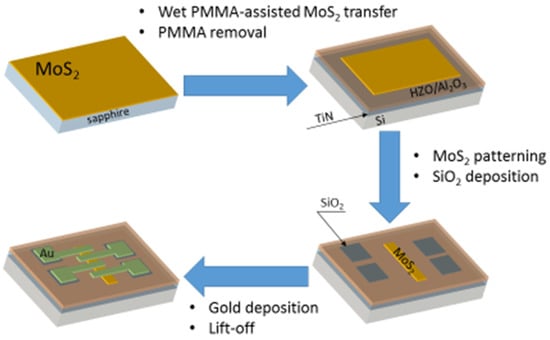
Figure 1.
The process flow schematic of FET structure fabrication.
A similar FET structure based on an exfoliated MoS2 flake was also prepared as a reference device. For transfer length method (TLM) measurements, four evenly spaced contacts to the MoS2 channel were patterned. Electrical characterization was carried out using the Keysight B1500A measuring unit, connected to a Cascade Microtech Summit probe station.
3. Results and Discussion
First, the chemical state and the thickness of the grown MoO3 film were investigated by XPS. In order to avoid surface contamination, the sample was in situ transferred to an XPS analysis chamber immediately after ALD growth. The collected Mo3d and O1s XPS spectra are presented in Figure 2. The Mo3d spectrum is well described by two doublets, corresponding to the Mo6+ and Mo5+ oxidation states (Figure 2a) with binding energies of Mo3d5/2 line 233.2 eV and 232.0 eV, respectively. This observation clearly indicates the slight oxygen deficiency in the grown film, since the non-lattice component can be found in the O1s spectrum (Figure 2b), and the VB spectrum demonstrates a visible peak in the bandgap (not shown), corresponding to the oxygen vacancy presence [47,48].The calculated O/Mo ratio was found to be ≈2.9. Since the carbon and nitrogen content in the grown film was found to be below the XPS detection limit, the observed oxygen deficiency can be eliminated by longer O3 exposure during growth. However, since the subsequent sulfurization step takes place in a hydrogen-containing atmosphere, this can be neglected.
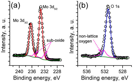
Figure 2.
Mo3d (a) and O1s (b) XPS spectra of the initial MoO3 film.
The XPS analysis carried out immediately after sulfurization (Figure 3a,b) revealed that the Mo3d spectrum is described by a single doublet with the binding energy of the Mo3d5/2 line of approximately 229.6 eV, which corresponds to the Mo4+ state in MoS2 [27]. In addition, no peaks corresponding to the state of Mo being bonded with oxygen ions are observed, suggesting the complete conversion of the MoO3 to Mo-sulfide. The corresponding S2p spectrum consists of a single doublet with the binding energy of the S2p3/2 line at 162.4 eV, which coincides with the stoichiometric MoS2. The quantitative XPS analysis based on Mo3d and S2p sensitivity factors showed that the film stoichiometry was S/Mo ≈ 2.1 for the given sulfurization conditions. In order to estimate the obtained MoS2 thickness and continuity, the XPS spectra corresponding to the film and substrate were collected in the angle-resolved mode (Figure 3c). According to our previous work, such a procedure possesses sufficient accuracy [31]. It was found that the best fitting experimental data correspond to a continuous film (f ≈ 0.93) with a thickness of ≈2.2 nm (3–4 MoS2 monolayers).
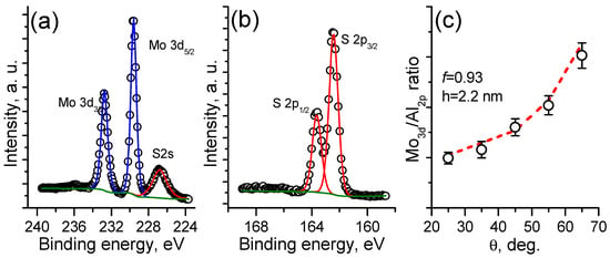
Figure 3.
XPS spectra of Mo3d (a) and S2p (b) lines measured from the sulfurized MoO3 film; Mo3d/Al2p signal ratio as a function of the electron emission angle Θ (c).
Next, the sulfurized film was investigated by atomic force microscopy (AFM) and transmission electron microscopy (TEM). It was found that the obtained MoS2 film was quite smooth, with the measured root-mean-square value of only 0.33 nm (Figure 4a), which is significantly lower than the value obtained in our previous work [28]. Furthermore, the film was found to be continuous and uniform since crystalline grains were not resolved. For the TEM analysis, the MoS2 film was transferred from the sapphire to a copper grid. The obtained plan-view TEM image is presented in Figure 4b.
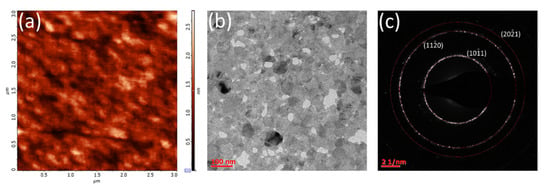
Figure 4.
AFM (a) and plan-view TEM (b) images and selected-area electron diffraction (SAED) pattern (c) of MoS2 film, obtained via MoO3 sulfurization.
The TEM analysis confirmed the polycrystalline nature of the obtained MoS2 film, which consists of grains with sizes in the range of 20–100 nm. However, the weakness of the bonds between them caused the loss of some grains during the film transfer, which is, apparently, the main reason for the observed local discontinuity. The basal planes of the grains seem to be aligned to the substrate surface, while no signs of the edge-terminated structure are observed. Obviously, the related SAED image (Figure 4c) contains only dot-like (10–11) and (11–20) diffraction rings. The absence of the diffraction ring corresponding to the (0001) plane of MoS2 confirms that all observed grains have their [0001] direction aligned with the out-of-plane direction, while their in-plane orientations are almost random.
The spectroscopic Raman analysis of the obtained MoS2 film and exfoliated reference flake (Figure 5) was carried out on the resonant excitation wavelength (632.8 nm) corresponding to the direct bandgap (1.96 eV). Under these conditions, the obtained spectra contain first-order peaks denoted as E2g1 (Г) and A1g (Г) corresponding to oscillatory modes inside the S-Mo-S layer in the parallel and perpendicular directions, but also overtones and combination peaks. For the sulfurized film, the difference between A1g and E2g1 peaks was found to be approximately 23.7 cm−1, corresponding to the multilayer [49] MoS2, which is consistent with XPS thickness estimation. On the reference flake spectrum, the difference between these modes is 23.2 cm−1, which corresponds to three MoS2 monolayers.
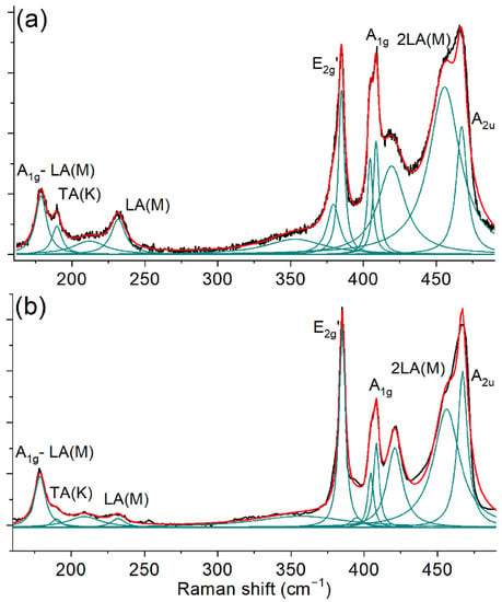
Figure 5.
Raman spectra of MoS2: (a) Sulfurized MoO3 film; (b) exfoliated reference flake.
The most significant differences between the discussed spectra are observed in the range from approximately 180 cm−1 to approximately 250 cm−1 containing several peaks (TA(K) ≈ 182 cm−1, LA(M) ≈ 227 cm−1), which are sensitive to lattice defects [50]. These modes cannot be observed in the spectra of the perfect MoS2 crystal structure, according to the momentum conservation rule. However, it can be satisfied by the phonon scattering from a defect, enabling the observation of zone-edge modes by Raman measurement [51]. The relative LA(M)/E2g1 (Г) intensity ratio was found to be approximately 5 times higher for the sulfurized film compared to the flake, which indicates a higher concentration of defects. For microcrystalline MoS2 films, the main type of defects is usually the crystalline domain boundaries. Therefore, the relative intensity of the LA(M) peak correlates with the size of the domains in accordance with earlier reports [28]. In general, the spectrum of the sulfurized film is typical for the structure containing sub-µm grains [52].
After the basic MoS2 film characterization, four field-effect transistor devices with MoS2 channels were fabricated and investigated. Three structures were based on the films obtained via sulfurization, while the reference one was based on the exfoliated flake. DC-IV source-drain characteristics measured at different gate voltages are presented in Figure 6a,c for sulfurized and flake-based devices, respectively.
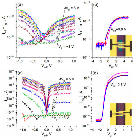
Figure 6.
DC-IV source-drain characteristics of FETs based on sulfurized (a) and flake (c) MoS2 with a channel length of 1 µm measured at different gate voltages; transfer characteristics (b,d) of mentioned FETs (different colors correspond to nominally identical structures) measured at Vsd = 0.8 V (inset: Optical image of the FET).
All observed FET characteristics (Figure 6a,c) indicate the n-type MoS2 behavior since applying positive gate voltage resulted in a visible increase in channel conductivity. However, in the case of sulfurized MoS2 films, the applied gate voltage was strongly limited by leakages due to the high FET structure resistivity. As a result, the maximum achieved current modulation was found to be ≈40 (Figure 6b), which is comparable to the existing literature data [36,40,44]. For instance, Schram et al. reported a small ambipolar response with a weak (Ion/Ioff ≈ 3) gate modulation for CVD-grown WS2 nanolayers [40]. In contrast, plasma-enhanced ALD for WS2 growth with a technique of seed density inhibition for the larger crystalline size achievement resulted in a significant (up to 103 times) modulation improvement. The authors ascribed such a difference to the specifics of CVD growth, namely, the surface-mediated reaction of the WF6 precursor with a sacrificial Si layer, which limited the crystal grain size and orientation. Similar microcrystalline MoS2 layers obtained by sputtering with additional sulfur powder annealing showed an Ion/Ioff ratio ≈ 30, which was limited by the remaining parasitic resistance [44]. The experiments of Matsuura et al. also revealed the necessity of sulfur vacancy healing to obtain any field effect. Despite this observation, here we reasonably guess that the sulfurization technique can hardly yield a significant sulfur deficiency (Figure 3). To date, the most prominent study of such films was carried out by Mahlouji et al., where thickness scaling and contact engineering were both considered [36,46]. It was found that the modulation magnitude has a strong maximum (Ion/IOff ≈ 2 × 10⁴) at a film thickness of ≈1.2 nm. Despite the fact that the observed discontinuity of such a thin film resulted in the presence of side contacts to MoS2, which has practical merit, its repeatability may be quite challenging. Furthermore, the contact engineering results were found to be not invariant in relation to a film thickness making further studies necessary.
In comparison, the electrical characteristics of the flake-based FET were found to be significantly superior, namely, it demonstrated four orders of magnitude greater Ion current (Figure 6d), which made leakage current contribution negligible (Ion/Ioff ~ 5 × 10⁴). According to the extracted subthreshold slope (SS) (320 mV/dec), field effect mobility was found to be ~0.4 cm2/Vs. The key extracted performance parameters for FET structures are summarized in Table 1.

Table 1.
FET structures performance parameters for sulfurized MoS2-based FETs and flake-based FETs.
In order to reveal the basic reason for the observed difference between the discussed films, additional TLM measurements, allowing us to separate the intrinsic MoS2 resistance and the contact resistance, were carried out.
It was found that sulfurized MoS2-based FET resistivity linearly depends on the channel length. The corresponding sheet resistance of the MoS2 film was found to be ≈160 GΩ/sq (Figure 7a). As it has already been demonstrated, grain boundaries affect the electrical properties of polycrystalline MoS2 films significantly [12,53,54]. This typically manifests in a strong correlation between the carrier mobility and the IOn/IOff ratio and line defect density. Therefore, we can conclude that the intrinsic conductivity of the investigated MoS2 films is inferior to those reported in the literature [36,46] partially due to the relatively small grain size (Figure 4b) and their misorientation. In particular, the MoS2-based FET performance can be described by the normalized mean Ion current. For instance, the Ion current for a multiple-layer exfoliated MoS2 transistor was reported to be ~103 µA/µm [55,56]. Simultaneously, microcrystalline MoS2 films showed significantly lower values—down to ≈10 µA/µm [36], which may be strongly governed by the source/drain-MoS2 contact quality [46]. Despite the fact that, in these works, the contribution of MoS2 resistance itself was not evaluated, it should be noted that the achieved Ion current was ~105 times higher than in our case.
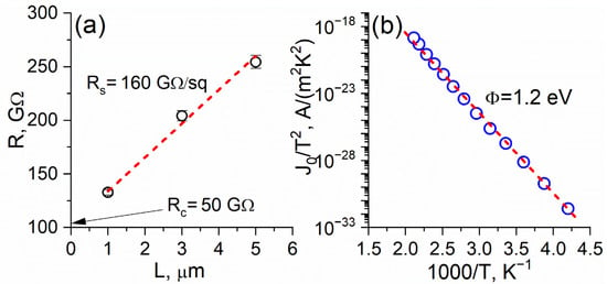
Figure 7.
(a) Sulfurized MoS2-based FET resistivity as a function of channel length; (b) Arrhenius plot of J0/T2 as a function of 1/T used for calculating the effective Schottky barrier height using the thermionic emission model.
However, the main factor limiting the sulfurized MoS2-based FETs performance was the contact resistivity (ρc). According to Figure 6a, the ρc value was found to be approximately 4 × 10³ Ω·cm2 indicating the presence of a high Schottky barrier at the MoS2/Au interface [57,58]. The barrier height was calculated from the Arrhenius plot slope (Figure 7b) [59] and the result was ≈1.2 eV. The key role of contact resistance was further supported by the analysis of the reference device characteristics. The corresponding ρc value measured on the flake-based FET was found to be several orders of magnitude lower, which resulted in a barrier height comparable to the literature-reported value of ≈0.13 eV [60]. Therefore, in contrast to the natural MoS2 crystal, much more careful contact metal selection is necessary to demonstrate the full potential of the MoS2 film obtained via the sulfurization technique. Moreover, the MoS2 grain size increase is highly desired since it should naturally improve the mean current density. Previously, it was shown that the preliminary hydrogen treatment of the seed oxide film may significantly change the grain size distribution and reduce the WS2 resistivity [45]. Furthermore, the sulfurization temperature increase allowed the MoS2 grain size and orientation to vary between the edge-terminated (700 °C) and terrace-terminated structures (900 °C) [28]. Since, in both cases, two competing processes exist (oxide sublimation and sulfurization), changing the hydrogen treatment time and the sulfur supply parameters (start time, effective flow, and duration) may improve the resulting film performance. This may be a possible task for future research. Overall, such considerations confirm the necessity of detailed investigations into both contact and intrinsic properties of such microcrystalline material, since it might be of practical interest due to the fabrication simplicity and cost-effectiveness.
4. Conclusions
In this work, MoS2 films were obtained using a cost-effective method of sulfurization of thermal-ALD deposited MoO3. To estimate their performance, FET structures were fabricated and investigated, which demonstrated an Ion/Ioff ratio of ≈40. According to the experimental data, limiting factors were the polycrystalline structure and high contact resistance at the drain and source. These conclusions are supported by TEM grain size evaluation and Raman spectra featuring strong defect-attributed peaks as well as temperature-dependent conductivity behavior, which indicated a significant Schottky barrier influence on structure conductivity. The findings indicate the necessity of further careful development of fabrication processes including tuning sulfurization procedure parameters to increase grain size and careful contact metal selection based on the band structure investigations for films obtained via this technique. However, overall, due to its simplicity, cost-effectiveness, and low sensitivity to the substrate material, we still consider such a technique of MoS2 synthesis highly attractive for applications in next-generation electronics. The two-stage synthesis process described here may also be useful for the fabrication of other transition metal dichalcogenides ultrathin films (e.g., WS2).
Author Contributions
Conceptualization, A.M.M., methodology, A.M.M., I.V.Z., and M.G.K., device fabrication, I.V.Z.; reference device fabrication, I.V.Z., A.G.C., P.M., and A.V.A.; electrical characterization, I.V.Z.; XPS, M.G.K., and A.A.K.; Raman investigation, R.I.R., N.V.D., and V.S.V.; AFM, M.G.K., and A.G.C.; TEM data analysis, R.I.R.; data analysis and visualization, I.V.Z., M.G.K., and R.I.R.; writing—original draft preparation, M.G.K., and I.V.Z.; writing—review and editing, A.M.M., I.V.Z., M.G.K., and R.I.R.; supervision and project administration, A.M.M. All authors have read and agreed to the published version of the manuscript.
Funding
The main part of the work (MoS2 synthesis and its general inspection, FET fabrication, and its electrical characterization) was supported by the Russian Science Foundation (Project. No 19-19-00504-P). Raman spectroscopy measurements and the MoS2 crystal exfoliation experiment were supported by the Russian Science Foundation (Project. No 22-19-00738).
Data Availability Statement
Data are available at reasonable request from the authors.
Acknowledgments
The authors also acknowledge the Systems for microscopy and analysis for TEM analysis and MIPT Center of shared facilities for access to the equipment.
Conflicts of Interest
The authors declare no conflict of interest.
References
- Robinson, J.A. Perspective: 2D for beyond CMOS. APL Mater. 2018, 6, 058202. [Google Scholar] [CrossRef]
- Briggs, N.; Subramanian, S.; Lin, Z.; Li, X.; Zhang, X.; Zhang, K.; Xiao, K.; Geohegan, D.; Wallace, R.; Chen, L.-Q.; et al. A roadmap for electronic grade 2D materials. 2D Mater. 2019, 6, 022001. [Google Scholar] [CrossRef]
- Radisavljevic, B.; Radenovic, A.; Brivio, J.; Giacometti, V.; Kis, A. Single-layer MoS2 transistors. Nat. Nanotechnol. 2011, 6, 147–150. [Google Scholar] [CrossRef] [PubMed]
- Wang, Q.H.; Kalantar-Zadeh, K.; Kis, A.; Coleman, J.N.; Strano, M.S. Electronics and optoelectronics of two-dimensional transition metal dichalcogenides. Nat. Nanotechnol. 2012, 7, 699–712. [Google Scholar] [CrossRef]
- Voiry, D.; Yang, J.; Chhowala, M. Recent strategies for improving the catalytic activity of 2D TMD nanosheets toward the hydrogen evolution reaction. Adv. Mater. 2016, 28, 6197–6206. [Google Scholar] [CrossRef]
- Chen, X.; Liu, C.; Mao, S. Environmental analysis with 2D transition-metal-dichalcogenide-based field-effect transistors. Nano-Micro Lett. 2020, 12, 95. [Google Scholar] [CrossRef]
- Ovchinnikov, D.; Allain, A.; Huang, Y.-S.; Dumcenco, D.; Kis, A. Electrical transport properties of single-layer WS2. ACS Nano 2014, 8, 8174–8181. [Google Scholar] [CrossRef]
- Addou, R.; McDonell, S.; Barrerra, D.; Guo, Z.; Azcatl, A.; Wang, J.; Zhu, H.; Hunkle, C.L.; Quevedo-Lopez, M.; Alshareef, H.N.; et al. Impurities and Electronic Property Variations of Natural MoS2 Crystal Surfaces. ACS Nano 2015, 9, 9124–9133. [Google Scholar] [CrossRef]
- Pyeon, J.J.; Kim, S.H.; Jeong, D.S.; Baek, S.-H.; Kang, C.-Y.; Kim, J.-S.; Kim, S.K. Wafer-scale growth of MoS2 thin films by atomic layer deposition. Nanoscale 2016, 8, 10792–10798. [Google Scholar] [CrossRef]
- Jeon, W.; Cho, Y.; Jo, S.; Ahn, J.-H.; Jeong, S.-J. Wafer-Scale synthesis of reliable high-mobility molybdenum disulfide thin films via inhibitor-utilizing atomic layer deposition. Adv. Mater. 2017, 29, 1703031. [Google Scholar] [CrossRef]
- Sharma, A.; Verheijen, M.A.; Wu, L.; Karwal, S.; Vandalon, V.; Knoops, H.C.M.; Sundaram, R.S.; Hofmann, J.P.; Kessels, W.M.M.; Bol, A.A. Low-Temperature Plasma-Enhanced Atomic Layer Deposition of 2-D MoS2: Large Area, Thickness Control and Tuneable Morphology. Nanoscale 2018, 10, 8615–8627. [Google Scholar] [CrossRef] [PubMed]
- Dumcenco, D.; Ovchinnikov, D.; Marinov, K.; Lazic, P.; Gibertini, M.; Marzari, N.; Sanchez, O.L.; Kung, Y.-C.; Krasnozhon, D.; Chen, M.-W.; et al. Large-Area Epitaxial Monolayer MoS2. ACS Nano 2015, 9, 4611–4620. [Google Scholar] [CrossRef] [PubMed]
- Laskar, M.R.; Ma, L.; Kannappan, S.; Park, P.S.; Krishnamoorthy, S.; Nath, D.N.; Lu, W.; Wu, Y.; Rajan, S. Large area single crystal (0001) oriented MoS2. Appl. Phys. Lett. 2013, 102, 252108. [Google Scholar] [CrossRef]
- Chen, J.; Tang, W.; Tian, B.; Liu, B.; Zhao, X.; Liu, Y.; Ren, T.; Liu, W.; Geng, D.; Jeong, H.Y.; et al. Chemical Vapor Deposition of High-Quality Large-Sized MoS2 Crystals on Silicon Dioxide Substrates. Adv. Sci. 2016, 3, 1500033. [Google Scholar] [CrossRef]
- Kang, K.; Xie, S.; Huang, L.; Han, Y.; Huang, P.Y.; Mak, K.F.; Kim, C.-J.; Muller, D.; Park, J. High-mobility three-atom-thick semiconducting films with wafer-scale homogeneity. Nature 2015, 520, 656–660. [Google Scholar] [CrossRef]
- Lin, Y.-C.; Jariwala, B.; Bersch, B.M.; Xu, K.; Nie, Y.; Wang, B.; Eichfeld, S.M.; Zhang, X.; Choudhury, T.H.; Pan, Y.; et al. Realizing large-scale, electronic-grade two-dimensional semiconductors. ACS Nano 2018, 12, 965–975. [Google Scholar] [CrossRef]
- Lee, D.H.; Sim, Y.; Wang, J.; Kwon, S.-Y. Metal-organic chemical vapor deposition of 2D van der Waals materials-The challenges and the extensive future opportunities. APL Mater. 2020, 8, 030901. [Google Scholar] [CrossRef]
- Groven, B.; Mehta, A.N.; Bender, H.; Meersschaut, J.; Nuytten, T.; Verdonck, P.; Conard, T.; Smets, Q.; Schram, T.; Schoenaers, B.; et al. Two-Dimensional Crystal Grain Size Tuning in WS2 Atomic Layer Deposition: An Insight in the Nucleation Mechanism. Chem. Mater. 2018, 30, 7648–7663. [Google Scholar] [CrossRef]
- Balasubramanyam, S.; Shirazi, M.; Bloodgood, M.A.; Wu, L.; Verheijen, M.A.; Vandalon, V.; Kessels, W.M.M.; Hofmann, J.P.; Bol, A.A. Edge-site nanoengineering of WS2 by low-temperature plasma-enhanced atomic layer deposition for electrocatalytic hydrogen evolution. Chem. Mater. 2019, 31, 5104–5115. [Google Scholar] [CrossRef]
- Kim, T.; Mun, J.; Park, H.; Joung, D.; Diware, M.; Won, C.; Park, J.; Jeong, S.-H.; Kang, S.-W. Wafer-scale Production of Highly-Uniform Two-Dimensional MoS2 by Metal-Organic Chemical Vapor Deposition. Nanotechnology 2017, 28, 18LT01. [Google Scholar] [CrossRef]
- Kwak, T.; Lee, J.; So, B.; Choi, U.; Nam, O. Growth Behavior of Wafer-Scale Two-Dimensional MoS2 Layer Growth Using Metal-Organic Chemical Vapor Deposition. J. Cryst. Growth 2019, 510, 50–55. [Google Scholar] [CrossRef]
- Zhang, K.; Bersch, B.M.; Zhang, F.; Briggs, N.C.; Subramanian, S.; Xu, K.; Chubarov, M.; Wang, K.; Lerach, J.O.; Redwing, J.M.; et al. Considerations for Utilizing Sodium Chloride in Epitaxial Molybdenum Disulfide. ACS Appl. Mater. Interfaces 2018, 10, 40831–40837. [Google Scholar] [CrossRef] [PubMed]
- Kim, H.; Ovchinnikov, D.; Deiana, D.; Unuchek, D.; Kis, A. Suppressing Nucleation on Metal-Organic Chemical Vapor Deposition of MoS2 Monolayers by Alkali Metal Halides. Nano Lett. 2017, 17, 5056–5063. [Google Scholar] [CrossRef] [PubMed]
- Lin, Y.-C.; Zhang, W.; Huang, J.-K.; Liu, K.-K.; Lee, Y.-H.; Liang, C.-T.; Chu, C.-W.; Li, L.-J. Wafer-scale MoS2 thin layers prepared by MoO3 sulfurization. Nanoscale 2012, 4, 6637–6641. [Google Scholar] [CrossRef]
- Martella, C.; Melloni, P.; Cinquanta, E.; Cianci, E.; Alia, M.; Longo, M.; Lamperti, A.; Vangelista, S.; Fancuilli, M.; Molle, A. Engineering the Growth of MoS2 via Atomic Layer Deposition of Molybdenum Oxide Film Precursor. Adv. Electron. Mater. 2016, 2, 1600330. [Google Scholar] [CrossRef]
- Heyne, M.H.; Chiappe, D.; Meersschaut, J.; Nuytten, T.; Conard, T.; Bender, H.; Huyghbaert, C.; Radu, I.P.; Caymax, M.; de Marneffe, J.-F.; et al. Multilayer MoS2 growth by metal and metal oxide sulfurization. J. Mater. Chem. C 2016, 4, 1295–1304. [Google Scholar] [CrossRef]
- Vangelista, S.; Cinquanta, E.; Martella, C.; Alia, M.; Longo, M.; Lamperti, A.; Mantovan, R.; Basset, F.B.; Pezzoli, F.; Molle, A. Towards a uniform and large-scale deposition of MoS2 nanosheets via sulfurization of ultra-thin Mo-based solid films. Nanotechnology 2016, 27, 175703. [Google Scholar] [CrossRef]
- Romanov, R.I.; Kozodaev, M.G.; Myakota, D.I.; Chernikova, A.G.; Novikov, S.M.; Volkov, V.S.; Slavich, A.S.; Zarubin, S.S.; Chizhov, P.S.; Khakimov, R.R.; et al. Synthesis of Large Area Two-Dimensional MoS2 Films by Sulfurization of Atomic Layer Deposited MoO3 Thin Film for Nanoelectronic Applications. ACS Appl. Nano Mater. 2019, 2, 7521–7531. [Google Scholar] [CrossRef]
- Mackus, A.J.M.; Schneider, J.R.; MacIsaac, C.; Baker, J.G.; Bent, S.F. Synthesis of Doped, Ternary, and Quaternary Materials by Atomic Layer Deposition: A Review. Chem. Mater. 2019, 31, 1142–1183. [Google Scholar] [CrossRef]
- Knoops, H.C.M.; Faraz, T.; Arts, K.; Kessels, W.M.M. Status and Prospects of Plasma-Assisted Atomic Layer Deposition. J. Vac. Sci. Technol. A 2019, 37, 030902. [Google Scholar] [CrossRef]
- Kozodaev, M.G.; Romanov, R.I.; Chernikova, A.G.; Markeev, A.M. Atomic Layer Deposition of Ultrathin Tungsten Oxide Films from WH2(Cp)2 and Ozone. J. Phys. Chem. C 2021, 125, 21663–21669. [Google Scholar] [CrossRef]
- Lee, B.H.; Byunghoon, Y.; Abdulagatov, A.I.; Hall, R.A.; George, S.M. Growth and Properties of Hybrid Organic-Inorganic Metalcone Films using Molecular Layer Deposition Techniques. Adv. Funct. Mater. 2013, 23, 532–546. [Google Scholar] [CrossRef]
- Alekhin, A.P.; Chouprik, A.A.; Gudkova, S.A.; Markeev, A.M.; Lebedinskii, Y.Y.; Matveyev, Y.A.; Zenkevich, A.V. Structural and electrical properties of TixAl1-xOy thin films grown by atomic layer deposition. J. Vac. Sci. Technol. B 2011, 29, 01A302. [Google Scholar] [CrossRef]
- Kozodaev, M.G.; Chernikova, A.G.; Korostylev, E.V.; Park, M.H.; Khakimov, R.R.; Hwang, C.S.; Markeev, A.M. Mitigating wakeup effect and improving endurance of ferroelectric HfO2-ZrO2 thin films by careful La-doping. J. Appl. Phys. 2019, 125, 034101. [Google Scholar] [CrossRef]
- Zhang, H.; Arutchelvan, G.; Meerschaut, J.; Gaur, A.; Conard, T.; Bender, H.; Lin, D.; Asselberghs, I.; Heyns, M.; Radu, I.; et al. MoS2 Functionalization with a Sub-nm Thin SiO2 Layer for Atomic Layer Deposition of High-k Dielectrics. Chem. Mater. 2017, 29, 6772–6780. [Google Scholar] [CrossRef]
- Mahlouji, R.; Verheijen, M.A.; Zhang, Y.; Hofmann, J.P.; Kessels, W.M.M.; Bol, A.A. Thickness and Morphology Dependent Electrical Properties of ALD-Synthesized MoS2 FETs. Adv. Electron. Mater. 2022, 8, 2100781. [Google Scholar] [CrossRef]
- Lu, Y.; Chen, T.; Ryu, G.-H.; Huang, H.; Sheng, Y.; Chang, R.-J.; Warner, J.H. Self-Limiting Growth of High-Quality 2D Monolayer MoS2 by Direct Sulfurization Using Precursor-Soluble Substrates for Advanced Field-Effect Transistors and Photodetectors. ACS Appl. Nano Mater. 2019, 2, 369–378. [Google Scholar] [CrossRef]
- Liu, Y.; Gu, F. A Wafer-Scale Synthesis of Monolayer MoS2 and their field-effect transistors toward practical applications. Nanoscale Adv. 2021, 3, 2117–2138. [Google Scholar] [CrossRef]
- Romanov, R.I.; Kozodaev, M.G.; Chernikova, A.G.; Zabrosaev, I.V.; Chouprik, A.A.; Zarubin, S.S.; Novikov, S.M.; Volkov, V.S.; Markeev, A.M. Thickness-Dependent Structural and Electrical Properties of WS2 Nanosheets Obtained via the ALD-Grown WO3 Sulfurization Technique as a Channel Material for Field-Effect Transistors. ACS Omega 2021, 6, 34429–34437. [Google Scholar] [CrossRef]
- Schram, T.; Smets, Q.; Groven, B.; Heyne, M.H.; Kunnen, E.; Thiam, A.; Devriendt, K.; Delabie, A.; Lin, D.; Lux, M.; et al. WS2 transistors on 300 mm wafers with BEOL compatibility. In Proceedings of the IEEE 47th European Solid-State Device Research Conference, Leuven, Belgium, 11–14 September 2017. [Google Scholar]
- Shimizu, J.; Ohashi, T.; Matsuura, K.; Muneta, I.; Kakushima, K.; Tsutsui, K.; Ikarashi, N.; Wakabayashi, H. Low-carrier Density sputtered-MoS2 Film by H2S annealing for Normally-Off Accumulation-mode FET. In Proceedings of the IEEE Electron Devices Technology and Manufacturing Conference (EDTM), Toyama, Japan, 28 February–2 March 2017. [Google Scholar]
- Toyama, M.; Ohashi, T.; Matsuura, K.; Shimizu, J.; Muneta, I.; Kakushima, K.; Tsutsui, K.; Wakabayashi, H. Ohmic Contact between Titanium and Sputtered MoS2 Films Achieved by Forming-Gas Annealing. Jpn. J. Appl. Phys. 2018, 57, 07MA04. [Google Scholar] [CrossRef]
- Matsuura, K.; Hamada, M.; Hamada, T.; Tanigawa, H.; Sakamoto, T.; Cao, W.; Parto, C.; Hori, A.; Muneta, I.; Kawanago, T.; et al. Normally-Off Sputtered-MoS2 nMISFETs with MoSi2 Contact by Sulfur Powder Annealing and ALD Al2O3 Gate Dielectric for Chip Level Integration. In Proceedings of the IEEE International Workshop on Junction Technology, Kyoto, Japan, 6–7 June 2019. [Google Scholar]
- Matsuura, K.; Hamada, M.; Hamada, T.; Tanigawa, H.; Sakamoto, T.; Hori, A.; Muneta, I.; Kawanago, T.; Kakushima, K.; Tsutsui, K.; et al. Normally-Off Sputtered-MoS2 nMISFETs with TiN top-gate electrode all defined by optical lithography for chip-level integration. Jpn. J. Appl. Phys. 2020, 59, 080906. [Google Scholar] [CrossRef]
- Kozodaev, M.G.; Slavich, A.S.; Romanov, R.I.; Zarubin, S.S.; Markeev, A.M. Influence of Reducing Agent on Properties of Thin WS2 Nanosheets Prepared by Sulfurization of Atomic Layer Deposited WO3. J. Phys. Chem. C 2020, 124, 28169–28177. [Google Scholar] [CrossRef]
- Mahlouji, R.; Zhang, Y.; Verheijen, M.A.; Hofmann, J.P.; Kessels, W.M.M.; Sagade, A.A.; Bol, A.A. On the Contact Optimization of ALD-Based MoS2 FETs: Correlation of Processing Conditions and Interface Chemistry with Device Electrical Performance. ACS Appl. Electron. Mater. 2021, 3, 3185–3199. [Google Scholar] [CrossRef] [PubMed]
- Vos, M.F.J.; Macco, B.; Thiessen, N.F.W.; Bol, A.A.; Kessels, W.M.M. Atomic layer deposition of molybdenum oxide from (NtBu)2(NMe2)2Mo and O2 plasma. J. Vac. Sci. Technol. A 2016, 34, 01A103. [Google Scholar] [CrossRef]
- Romanov, R.I.; Kozodaev, M.G.; Lebedinskii, Y.Y.; Perevalov, T.V.; Slavich, A.S.; Hwang, C.S.; Markeev, A.M. Radical-Enhanced Atomic Layer Deposition of a Tungsten Oxide Film with the Tunable Oxygen Vacancy Concentration. J. Phys. Chem. C 2020, 124, 18156–18164. [Google Scholar] [CrossRef]
- Chakraborty, B.; Matte, H.S.S.R.; Sood, A.K.; Rao, C.N.R. Layer-Dependent Resonant Raman Scattering of a Few Layer MoS2. J. Raman Spectrosc. 2013, 44, 92–96. [Google Scholar] [CrossRef]
- Mignuzzi, S.; Pollard, A.J.; Bonini, N.; Brennan, B.; Gilmore, I.S.; Pimenta, M.A.; Richards, D.; Roy, D. Effect of disorder on Raman scattering of single-layer MoS2. Phys. Rev. B 2015, 91, 195411. [Google Scholar] [CrossRef]
- Li, J.; Su, W.; Chen, F.; Fu, L.; Ding, S.; Song, K.; Huang, X.; Zhang, L. Atypical Defect-Mediated Photoluminescence and Resonance Raman Spectroscopy of Monolayer WS2. J. Phys. Chem. C 2019, 123, 3900–3907. [Google Scholar] [CrossRef]
- Blanco, E.; Afanasiev, P.; Berhault, G.; Uzio, D.; Loridant, S. Resonance Raman spectroscopy as a probe of the crystallite size of MoS2 nanoparticles. Comptes Rendus Chim. 2016, 19, 1310–1314. [Google Scholar] [CrossRef]
- Van der Zande, A.M.; Huang, P.Y.; Chenet, D.A.; Berkelbach, T.C.; You, Y.; Lee, G.-H.; Heinz, T.F.; Reichman, D.R.; Muller, D.A.; Hone, J.C. Grains and Grain Boundaries in Highly Crystalline Monolayer Molybdenum Disulphide. Nat. Mater. 2013, 12, 554–561. [Google Scholar] [CrossRef] [PubMed]
- Najmaei, S.; Amani, M.; Chin, M.L.; Liu, Z.; Birdwell, A.G.; O’Regan, T.P.; Ajayan, P.M.; Dubey, M.; Lou, J. Electrical Transport Properties of Polycrystalline Monolayer Molybdenum Disulfide. ACS Nano 2014, 8, 7930–7937. [Google Scholar] [CrossRef]
- Yoon, Y.; Ganapathi, K.; Salahuddin, S. How Good Can Monolayer MoS2 transistors Be? Nano Lett. 2011, 11, 3768–3773. [Google Scholar] [CrossRef]
- Si, M.; Su, C.-J.; Jiang, C.; Conrad, N.J.; Zhou, H.; Maize, K.D.; Qiu, G.; Wu, C.-T.; Shakouri, A.; Alam, M.A.; et al. Steep-Slope Hysteresis-Free Negative Capacitance MoS2 Transistors. Nat. Nanotechnol. 2018, 13, 24–28. [Google Scholar] [CrossRef]
- Giubileo, F.; Di Bartolomeo, A. The Role of Contact resistance in Graphene Field-Effect Devices. Prog. Surf. Sci. 2017, 92, 143–175. [Google Scholar] [CrossRef]
- Ni, J.; Fu, Q.; Ostrikov, K.; Gu, X.; Nan, H.; Xiao, S. Status and Prospects of Ohmic Contacts on Two-Dimensional Semiconductors. Nanotechnology 2022, 33, 062005. [Google Scholar] [CrossRef]
- Jahangir, I.; Uddin, M.A.; Singh, A.K.; Koley, G.; Chandrashekhar, M.V.S. Richardson Constant and Electrostatics in Transfer-Free CVD-grown Few-Layer MoS2/Graphene Barristor with Schottky barrier Modulation >0.6eV. Appl. Phys. Lett. 2017, 111, 142101. [Google Scholar] [CrossRef]
- Kaushik, N.; Nipane, A.; Basheer, F.; Dubey, S.; Grover, S.; Deshmukh, M.M.; Lodha, S. Schottky Barrier Heights for Au and Pd contacts to MoS2. Appl. Phys. Lett. 2014, 105, 113505. [Google Scholar] [CrossRef]
Publisher’s Note: MDPI stays neutral with regard to jurisdictional claims in published maps and institutional affiliations. |
© 2022 by the authors. Licensee MDPI, Basel, Switzerland. This article is an open access article distributed under the terms and conditions of the Creative Commons Attribution (CC BY) license (https://creativecommons.org/licenses/by/4.0/).