
Role of Vacancy Defects in Reducing the Responsivity of AlGaN Schottky Barrier Ultraviolet Detectors

Abstract
:1. Introduction
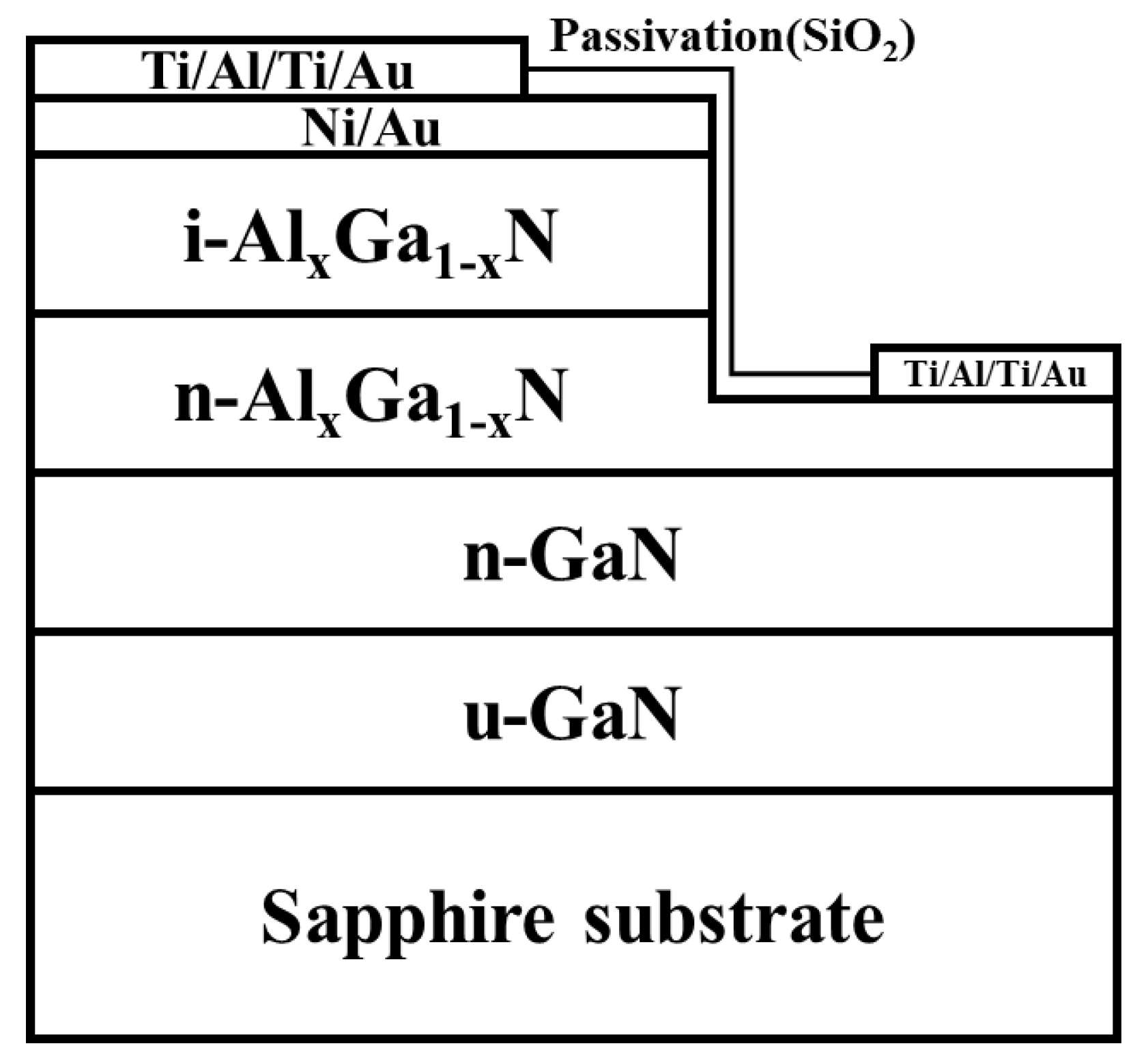
2. Experimental
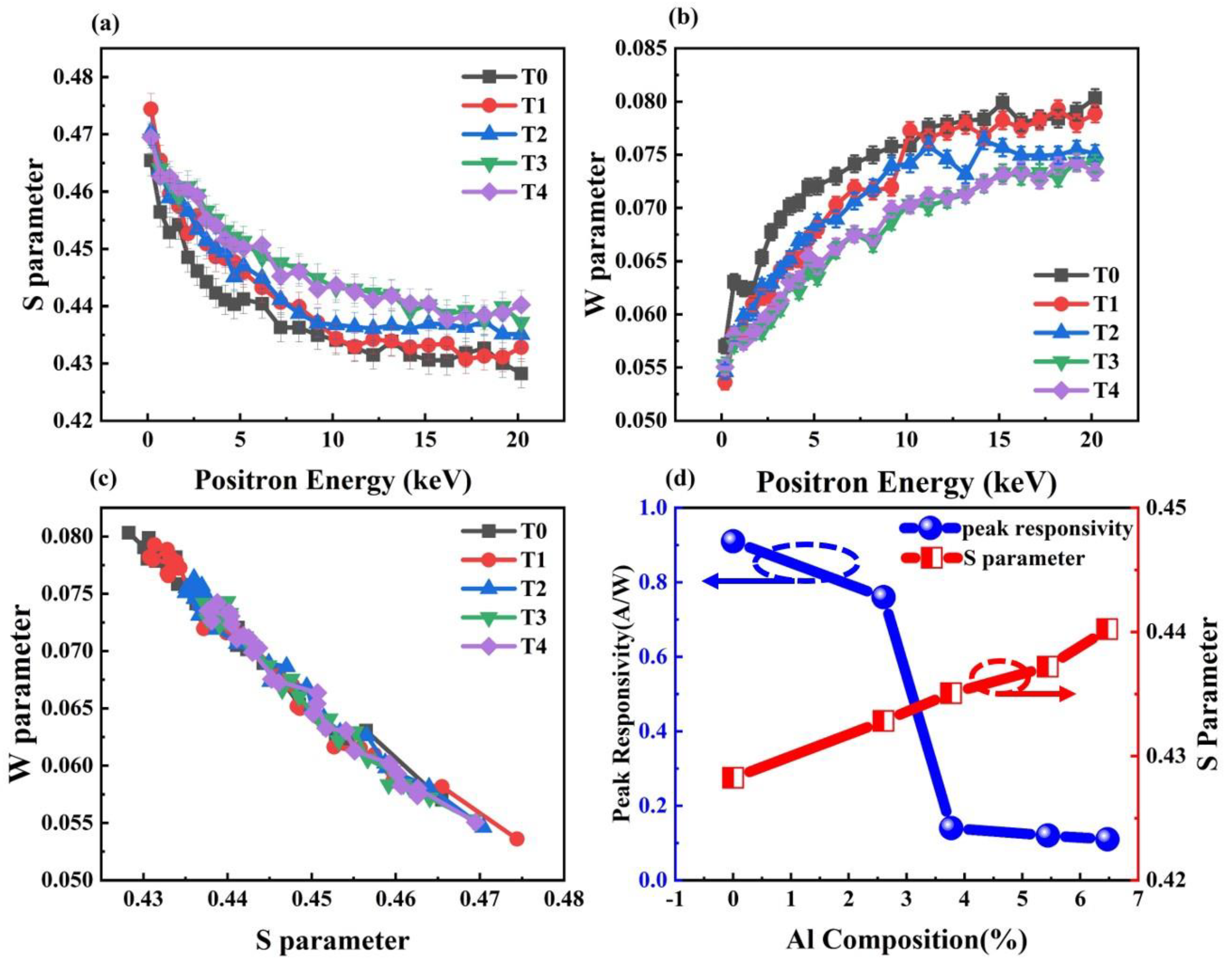
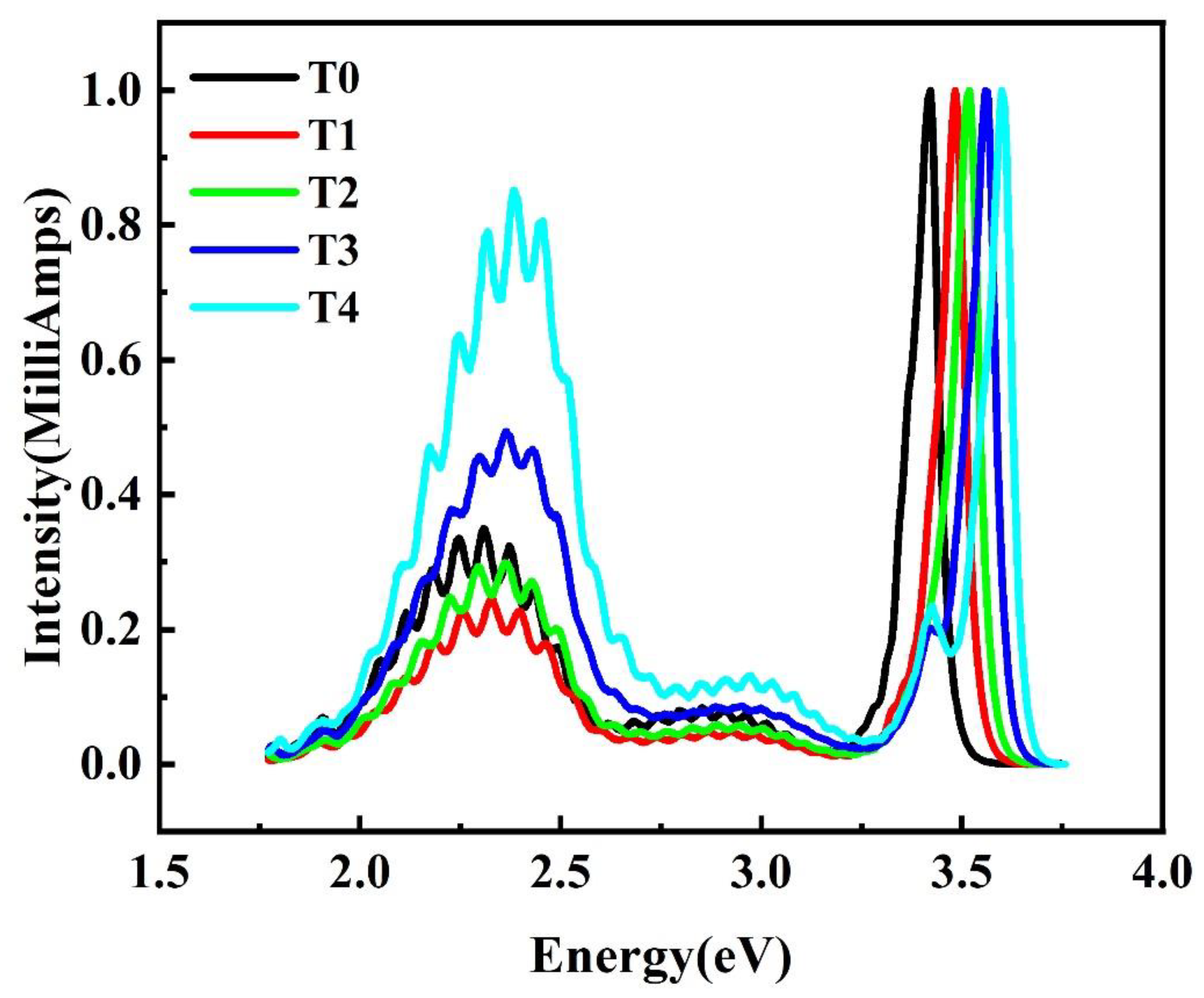
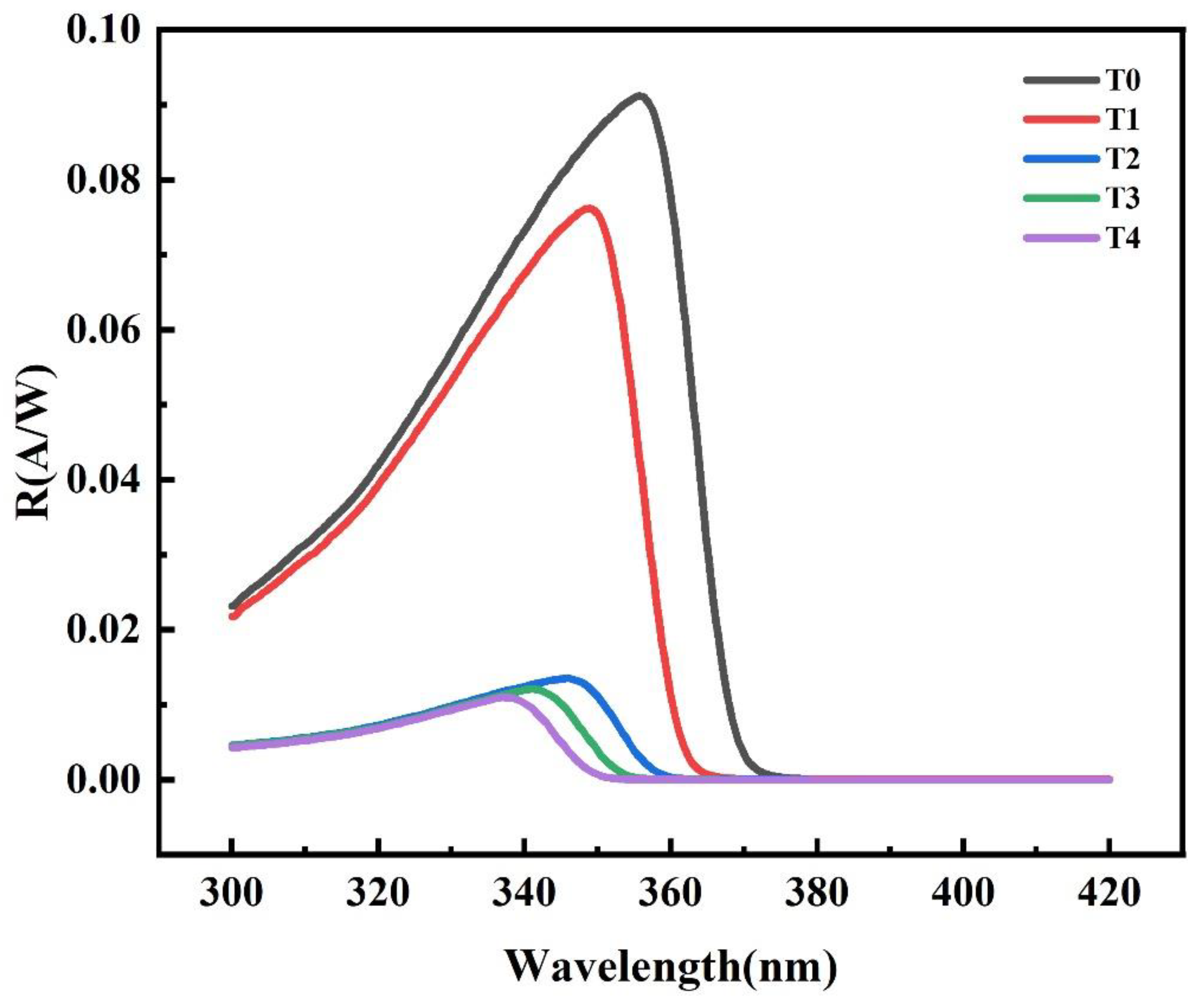
3. Results and Discussion
4. Conclusions
Author Contributions
Funding
Institutional Review Board Statement
Informed Consent Statement
Data Availability Statement
Conflicts of Interest
Ethical Compliance
References
- Gu, W.; Liu, Z.; Guo, Y.; Wang, X.; Jia, X.; Liu, X.; Zeng, Y.; Wang, J.; Li, J.; Yan, J. Comprehensive study of crystalline AlN/sapphire templates after high-temperature annealing with various sputtering conditions. J. Semicond. 2020, 41, 122802. [Google Scholar] [CrossRef]
- Guo, L.; Guo, Y.; Wang, J.; Wei, T. Ultraviolet communication technique and its application. J. Semicond. 2021, 42, 081801. [Google Scholar] [CrossRef]
- Yang, J.; Zhao, D.; Liu, Z.; Liang, F.; Chen, P.; Duan, L.; Wang, H.; Shi, Y. A 357.9 nm GaN/AlGaN multiple quantum well ultraviolet laser diode. J. Semicond. 2022, 43, 010501. [Google Scholar] [CrossRef]
- Alaie, Z.; Nejad, S.M.; Yousefi, M.H. Recent advances in ultraviolet photodetectors. Mater. Sci. Semicond. Processing 2015, 29, 16–55. [Google Scholar] [CrossRef]
- Chen, Q.; Yang, J.; Khan, M.A.; Sun, C. Visible-blind ultraviolet photodetectors based on GaN p-n junctions. Electron. Lett. 1995, 31, 1781–1782. [Google Scholar] [CrossRef]
- McClintock, R.; Yasan, A.; Mayes, K.; Shiell, D.; Darvish, S.R.; Kung, P.; Razeghi, M. High quantum efficiency AlGaN solar-blind p-i-n photodiodes. Appl. Phys. Lett. 2004, 84, 1248–1250. [Google Scholar] [CrossRef]
- Jiang, H.; Egawa, T. Low-Dark-Current High-Performance AlGaN Solar-Blind p–i–n Photodiodes. Jpn. J. Appl. Phys. 2008, 47, 1541–1543. [Google Scholar] [CrossRef]
- Zhao, D.G.; Zhang, S.; Jiang, D.S.; Zhu, J.J.; Liu, Z.S.; Wang, H.; Zhang, B.S.; Yang, H. A study on the spectral response of back-illuminated p-i-n AlGaN heterojunction ultraviolet photodetector. J. Appl. Phys. 2011, 110, 053701. [Google Scholar] [CrossRef]
- Wang, C.-K.; Chiou, Y.-Z.; Chang, S.-J.; Lai, W.-C.; Chang, S.-P.; Yen, C.-H.; Hung, C.-C. GaN MSM UV Photodetector with Sputtered AlN Nucleation Layer. IEEE Sens. J. 2015, 15, 4743–4748. [Google Scholar] [CrossRef]
- Biyikli, N.; Kimukin, I.; Kartaloglu, T.; Aytur, O.; Ozbay, E. High-speed solar-blind photodetectors with indium-tin-oxide Schottky contacts. Appl. Phys. Lett. 2003, 82, 2344–2346. [Google Scholar] [CrossRef]
- Li, J.; Zhao, M.; Wang, X. High performance Schottky UV photodetectors based on epitaxial AlGaN thin film. Phys. B Condens. Matter 2009, 405, 996–998. [Google Scholar] [CrossRef]
- Bouzid, F.; Dehimi, L.; Pezzimenti, F. Performance analysis of a Pt/n-GaN Schottky barrier UV detector. J. Electron. Mater. 2017, 46, 6563–6570. [Google Scholar] [CrossRef]
- Li, X.; Zhao, D.; Jiang, D.; Chen, P.; Zhu, J.; Liu, Z.; Le, L.; Yang, J.; He, X.; Zhang, L.; et al. Influence of residual carbon impurities in i-GaN layer on the performance of GaN-based p-i-n photodetectors. J. Vac. Sci. Technol. B Nanotechnol. Microelectron. Mater. Processing Meas. Phenom. 2016, 34, 011204. [Google Scholar] [CrossRef]
- Linkai, Y.; Haoran, Q.; Jialin, H.; Mei, Z.; Degang, Z.; Desheng, J.; Jing, Y.; Wei, L.; Feng, L. Influence of dislocation density and carbon impurities in i-GaN layer on the performance of Schottky barrier ultraviolet photodetectors. Mater. Res. Express 2018, 5, 046207. [Google Scholar] [CrossRef]
- Wang, W.; Yang, Z.; Lu, Z.; Li, G. High responsivity and low dark current nonpolar GaN-based ultraviolet photo-detectors. J. Mater. Chem. C 2018, 6, 6641–6646. [Google Scholar] [CrossRef]
- Henry, T.A.; Armstrong, A.; Allerman, A.A.; Crawford, M.H. The influence of Al composition on point defect incorporation in AlGaN. Appl. Phys. Lett. 2012, 100, 043509. [Google Scholar] [CrossRef]
- Heinke, H.; Kirchner, V.; Einfeldt, S.; Hommel, D. X-ray diffraction analysis of the defect structure in epitaxial GaN. Appl. Phys. Lett. 2000, 77, 2145–2147. [Google Scholar] [CrossRef]
- Dupasquier, A.; Mills, A.P., Jr. Positron Spectroscopy of Solids; IOS Press: Amsterdam, The Netherlands, 1995. [Google Scholar]
- Zhao, D.G.; Jiang, D.S.; Yang, H.; Zhu, J.J.; Liu, Z.S.; Zhang, S.M.; Liang, J.W.; Hao, X.P.; Wei, L.; Li, X.Y.; et al. Effect of lightly Si doping on the minority carrier diffusion length in n-type GaN films. Appl. Phys. Lett. 2006, 88, 252101. [Google Scholar] [CrossRef]
- Saarinen, K.; Laine, T.; Kuisma, S.; Nissilä, J.; Hautojärvi, P.; Dobrzynski, L.; Baranowski, J.M.; Pakula, K.; Stepniewski, R.; Wojdak, M.; et al. Observation Of Native Ga Vacancies In Gan By Positron Annihilation. MRS Proc. 1997, 482, 757. [Google Scholar] [CrossRef]
- Saarinen, K.; Seppälä, P.; Oila, J.; Hautojärvi, P.; Corbel, C.; Briot, O.; Aulombard, R.L. Gallium vacancies and the growth stoichiometry of GaN studied by positron annihilation spectroscopy. Appl. Phys. Lett. 1998, 73, 3253–3255. [Google Scholar] [CrossRef]
- Warnick, K.H.; Puzyrev, Y.; Roy, T.; Fleetwood, D.M.; Schrimpf, R.D.; Pantelides, S.T. Room-temperature diffusive phenomena in semiconductors: The case of AlGaN. Phys. Rev. B 2011, 84, 214109. [Google Scholar] [CrossRef]
- Puzyrev, Y.S.; Roy, T.; Beck, M.; Tuttle, B.R.; Schrimpf, R.; Fleetwood, D.M.; Pantelides, S.T. Dehydrogenation of defects and hot-electron degradation in GaN high-electron-mobility transistors. J. Appl. Phys. 2011, 109, 034501. [Google Scholar] [CrossRef]
- Zhao, D.G.; Jiang, D.S.; Zhu, J.J.; Liu, Z.S.; Zhang, S.M.; Liang, J.W.; Yang, H.; Li, X.; Li, X.Y.; Gong, H.M. Influence of defects in n−-GaN layer on the responsivity of Schottky barrier ultraviolet photodetectors. Appl. Phys. Lett. 2007, 90, 062106. [Google Scholar] [CrossRef]
- Liang, F.; Zhao, D.; Jiang, D.; Liu, Z.; Zhu, J.; Chen, P.; Yang, J.; Liu, S.; Xing, Y.; Zhang, L.; et al. Carbon-Related Defects as a Source for the Enhancement of Yellow Luminescence of Unintentionally Doped GaN. Nanomaterials 2018, 8, 744. [Google Scholar] [CrossRef]
- Yonenaga, I.; Ohno, Y.; Yao, T.; Edagawa, K. Optical and electrical properties of dislocations in plastically deformed GaN. J. Cryst. Growth 2014, 403, 72–76. [Google Scholar] [CrossRef]
- Armitage, R.; Hong, W.; Yang, Q.; Feick, H.; Gebauer, J.; Weber, E.R.; Hautakangas, S.; Saarinen, K. Contributions from gallium vacancies and carbon-related defects to the “yellow luminescence” in GaN. Appl. Phys. Lett. 2003, 82, 3457–3459. [Google Scholar] [CrossRef]


| Sample | TMGa Flux (umol/min) | TMAl Flux (umol/min) | Al Content (%) | FWHM of HRXRD (arc sec) | Carbon Impurity (atom/cm3) | Oxygen Impurity (atom/cm3) | Vacancy Concentration (/cm3) | Peak Responsivity (A/W) | |
|---|---|---|---|---|---|---|---|---|---|
| (002) | (102) | ||||||||
| T0 | 203 | 0 | 0 | 291 | 310 | 0.091 | |||
| T1 | 81 | 2.00 | 2.60 | 298 | 306 | 0.076 | |||
| T2 | 81 | 3.00 | 3.77 | 283 | 301 | 0.014 | |||
| T3 | 81 | 4.50 | 5.44 | 284 | 304 | 0.012 | |||
| T4 | 81 | 6.00 | 6.47 | 275 | 310 | 0.011 | |||
Publisher’s Note: MDPI stays neutral with regard to jurisdictional claims in published maps and institutional affiliations. |
© 2022 by the authors. Licensee MDPI, Basel, Switzerland. This article is an open access article distributed under the terms and conditions of the Creative Commons Attribution (CC BY) license (https://creativecommons.org/licenses/by/4.0/).
Share and Cite
Huang, Y.; Yang, J.; Zhao, D.; Zhang, Y.; Liu, Z.; Liang, F.; Chen, P. Role of Vacancy Defects in Reducing the Responsivity of AlGaN Schottky Barrier Ultraviolet Detectors. Nanomaterials 2022, 12, 3148. https://doi.org/10.3390/nano12183148
Huang Y, Yang J, Zhao D, Zhang Y, Liu Z, Liang F, Chen P. Role of Vacancy Defects in Reducing the Responsivity of AlGaN Schottky Barrier Ultraviolet Detectors. Nanomaterials. 2022; 12(18):3148. https://doi.org/10.3390/nano12183148
Chicago/Turabian StyleHuang, Yujie, Jing Yang, Degang Zhao, Yuheng Zhang, Zongshun Liu, Feng Liang, and Ping Chen. 2022. "Role of Vacancy Defects in Reducing the Responsivity of AlGaN Schottky Barrier Ultraviolet Detectors" Nanomaterials 12, no. 18: 3148. https://doi.org/10.3390/nano12183148
APA StyleHuang, Y., Yang, J., Zhao, D., Zhang, Y., Liu, Z., Liang, F., & Chen, P. (2022). Role of Vacancy Defects in Reducing the Responsivity of AlGaN Schottky Barrier Ultraviolet Detectors. Nanomaterials, 12(18), 3148. https://doi.org/10.3390/nano12183148