Article

Enhancing the Efficiency of Perovskite Solar Cells through Interface Engineering with MoS2 Quantum Dots

1
Key Laboratory of Automobile Materials MOE, School of Materials Science & Engineering, Jilin Provincial International Cooperation Key Laboratory of High-Efficiency Clean Energy Materials, Electron Microscopy Center, Jilin University, Changchun 130012, China
2
College of Electronic Science and Engineering, Jilin University, Changchun 130012, China
*
Authors to whom correspondence should be addressed.
These authors contributed equally to this work.
Nanomaterials 2022, 12(17), 3079; https://doi.org/10.3390/nano12173079
Submission received: 26 July 2022 / Revised: 24 August 2022 / Accepted: 1 September 2022 / Published: 5 September 2022
(This article belongs to the Special Issue Luminescent Colloidal Nanocrystals)

Abstract

:
The interface of perovskite solar cells (PSCs) determines their power conversion efficiency (PCE). Here, the buried bottom surface of a perovskite film is efficiently passivated by using MoS2 quantum dots. The perovskite films prepared on top of MoS2-assisted substrates show enhanced crystallinity, as evidenced by improved photoluminescence and a prolonged emission lifetime. MoS2 quantum dots with a large bandgap of 2.68 eV not only facilitate hole collection but also prevent the photogenerated electrons from flowing to the hole transport layer. Overall promotion leads to decreased trap density and an enhanced built-in electric field, thus increasing the device PCE from 17.87% to 19.95%.

Graphical Abstract

1. Introduction

Perovskite solar cells (PSCs) have been widely explored in recent years due to their low cost and high efficiency [1]. Notably, inverted-structure devices have shown negligible hysteresis and high stability due to the employment of undoped hole transport materials [2]. However, their power conversion efficiency (PCE) still lags that of normal structure devices, mainly due to the energy and carrier losses at the interface between the hole transport layer (HTL) and the perovskite active layer [3]. Although replacing the typical poly(3,4-ethylenedioxythiophene)s (PEDOT:PSS) with poly[bis (4-phenyl) (2,4,6- trimethylphenyl)amine] (PTAA) can significantly suppress interface losses [4], there is still a large number of voids and defects at the buried bottom surface of the perovskite layer. This is caused by the hydrophobicity of PTAA film, which serves as a substrate affecting the growth of perovskites. Degradation is more likely to happen at trap centers than inside the crystal under illumination, an electric field, and humidity conditions. Thus, buried interfacial voids and defects will serve as decomposition centers that accelerate device efficiency decline [5].
The interface between the HTL and the perovskite layer determines the hole transfer rate and hole collection efficiency [6], which can be significantly improved by enhancing the coupling between layers [7]. Moreover, interface engineering with various materials, including polymers [8,9,10], large organic cations [11,12], fullerene derivatives [13,14], carbon dots [15,16], and quantum dots (QDs) [17], can also block the undesired charge carrier flow, passivate surface traps, and improve the interface contact.
Molybdenum disulfide (MoS2), with high charge carrier mobilities and a tunable energy band structure, is a promising low dimensional material used in optoelectronic applications. The lattice of MoS2 and MAPbI3 (MA, methylamine) perovskites match well with each other, so they can form high-quality heterojunctions via epitaxy growth [18], being beneficial for reducing non-radiative recombination. MoS2 has been used mainly as a hole-transporting layer or dopant in these layers [19,20]. However, it is difficult to adjust the chemical properties of most MoS2 used in photoelectric devices [21]. Meanwhile, stacking 2D MoS2 reduces interface contact and easily causes a void at the interface.
Rich chemistry and size effects make QDs unique 0D materials with huge possibilities to tune their electronic properties and enhance device interface contact. Leyla et al. utilized MoS2 QDs with reduce graphene oxide (RGO) hybrids as hole transport layers (HTLs) and active buffer layers. The final PCE of the normal structure PSCs with MoS2 quantum dot/graphene hybrids reached 20.12% [22]. Here, we engineer the interface between perovskite and PTAA using MoS2 QDs, which passivates the buried defects, facilitates interface contact, promotes the perovskite crystal quality, prevents reverse carrier flow, and enhances hole collection. The MoS2 QDs are capped with trioctyl-phosphine oxide (TOPO). With optimized MoS2 QD layers, the PCE of perovskite solar cells increases from 17.87% to 19.95%, demonstrating that MoS2 QDs are indeed promising materials for passivating the buried defects of solution-processed perovskite optoelectronic devices.

2. Materials and Methods

Lead iodide (PbI2), lead bromide (PbBr2), formamidinium iodide (FAI), methylamium bromide (MABr), cesium iodide (CsI), and poly[bis(4-phenyl)(2,4,6-triMethylphenyl)aMine] (PTAA) were purchased from Xi’an Polymer Light Technology Corp (China). Bathocuproine (BCP) and (6,6)-phenyl C61-butyric acid methyl ester (PCBM) were purchased from Luminescence Technology Corp (Taiwan, China). N, N-dimethylformamide (DMF), dimethyl sulfoxide (DMSO), tri-n-octylphosphine (TOP), N-methylpyrrolidone (NMP) and sulfur were purchased from Sigma-Aldrich (Sigma-Aldrich, St. Louis, MO, USA). Ammonium molybdate tetrahydrate and cysteine were purchased from Sinopharm Chemical Reagent limited corporation (Beijing, China). Chlorobenzene (CB) was purchased from J&K Scientific Corp (Beijing, China). Silver was purchased from commercial sources with high purity.
The MoS2 QDs were synthesized using the hydrothermal method. Ammonium molybdate tetrahydrate (80.4 mg) and cysteine (20 mg) were dissolved in 10 mL NMP, heated, and stirred at 70 °C for 20 min. Sulfur (19.0 mg) was added into 2.5 mL TOP in a glove box before being stirred and heated at 70 °C until it was fully dissolved. Then, a 333 μL sulfur solution was added to the ammonium molybdate tetrahydrate NMP solution. Stirring and heating continued through the addition of 30 μL HCl (0.1 M) until the solution was transparent. The mixture was transferred to a Teflon reactor and heated continuously at 240 °C for 24 h. After cooling down to room temperature in the reactor, the obtained solution was poured into centrifuge tubes for centrifugation. The first-time centrifugation precipitate containing sulfur and bulk MoS2 was abandoned. The solution was then mixed with ethanol and centrifuged at 12,000 rpm for 20 min. The target product was obtained and dispersed in DMF for device fabrication.
Perovskite precursor was prepared by dissolving 506.9 mg PbI2, 80.7 mg PbBr2, 172.2 mg FAI, and 22.4 mg MABr in 1 mL of 4:1, v/v proportion dimethylformamide (DMF) and dimethyl sulfoxide (DMSO) mixture. The solution was heated at 70 °C until it became pellucid. Next, 42.4 μL as-prepared CsI (1.5M) DMSO solution with a concentration of 1.5 M was added to the as-mixed solution, which was left on a hotplate at 70 °C for 30 min. At this point, the precursor solution was ready for perovskite film preparation.
ITO substrates were cleaned using isopropyl alcohol, acetone, chloroform, acetone, and isopropyl alcohol in sequence, and all were treated with ultrasound for 10 min. Then, the ITO substrates were blow-dried with a dry nitrogen flow and treated with a vacuum plasma cleaner for 15 min. The PTAA (1.5 mg mL−1, in toluene) solution was spin-coated onto the pre-cleaned ITO substrates at 4000 rpm for 30s and heated at 100 °C for 10 min. After cooling down, 30 μL MoS2 QDs in different concentrations were spin-coated on PTAA layers at 4000 rpm for 8 s. Immediately, 70 μL perovskite precursor solution was dropped on the prewetted substrates. A two-stage spin-coating procedure was used for perovskite coating, 1000 rpm for 10 s and 6000 rpm for 20 s. During the second spin-coating step at 6000 rpm, 120 μL chlorobenzene was quickly dropped to the center of the wet film. After annealing at 100 °C for 10 min and cooling down to room temperature, PCBM (20 mg/mL) solution was dropped on the perovskite and spin-coated at 1500 rpm for 30 s and annealed at 100 °C for 10 min. Then, a 40 μL BCP (0.5 mg/mL in isopropanol) solution was dynamically dropped on the surface of the PCBM layer at a speed of 4000 rpm for 40 s. Finally, a Ag electrode was fabricated on the BCP layer using thermal evaporation depositing. The active area could be confirmed by the ITO and Ag electrode overlapping region of 0.047 cm−2.
X-ray diffraction (XRD) patterns were measured with a D8 Advance-Bruker AXS X system (Bruker AXS, Karlsruhe, Germany). Transmission electron microscopy (TEM) images were taken with a JEM 2100F TEM (Japan Electronics Co., Ltd, Japan). X-ray photoelectron spectroscopy (XPS) spectra were characterized with ESCALAB 250 (Thermo Fisher Scientific, Waltham, MA, USA). A previously reported method was referred to for the characterization of the interface [6]. Scanning electron microscope (SEM) images were taken using a Hitachi SU8000 SEM (Hitachi Limited, Tokyo, Japan) at 5 kV accelerating voltage. Steady-state photoluminescence spectra (PL) were acquired using an Ocean Insight USB4000 (Ocean Optics, Dunedin, FL, USA) with a 365 nm laser as the excitation light source. Absorption spectra were measured with a Shimadzu UV-1700 spectrometer (Shimadzu corporation, Kyoto, Japan). Fourier-transform infrared spectroscopy (FTIR) was conducted using a Nicolet IS50 FT-IR (Thermo Fisher Scientific, Waltham, MA, USA). Current density–voltage (J-V) and space-charge-limited current (SCLC) curves were measured using a Keithley 2400 Source Meter (Tektronix, Beaverton, OR, USA). All the current density-voltage measurements were conducted using a solar simulator (Class AAA solar simulator, Newport Technologies, Inc., Irvine, CA, USA) External quantum efficiency (EQE) curves were measured using a Crowntech QTest Station 1000 AD (Crowntech, INC., Indianapolis, IN, USA). Capacitance–voltage (C-V) curves were tested at a constant frequency of 100 kHz. Electrochemical impedance spectroscopy (EIS) was measured using an Admiral electrochemical workstation (Admiral Instruments, Tempe, AZ, USA) from 10 Hz to 1000 kHz frequency with 0.89 V bias voltage in dark conditions.

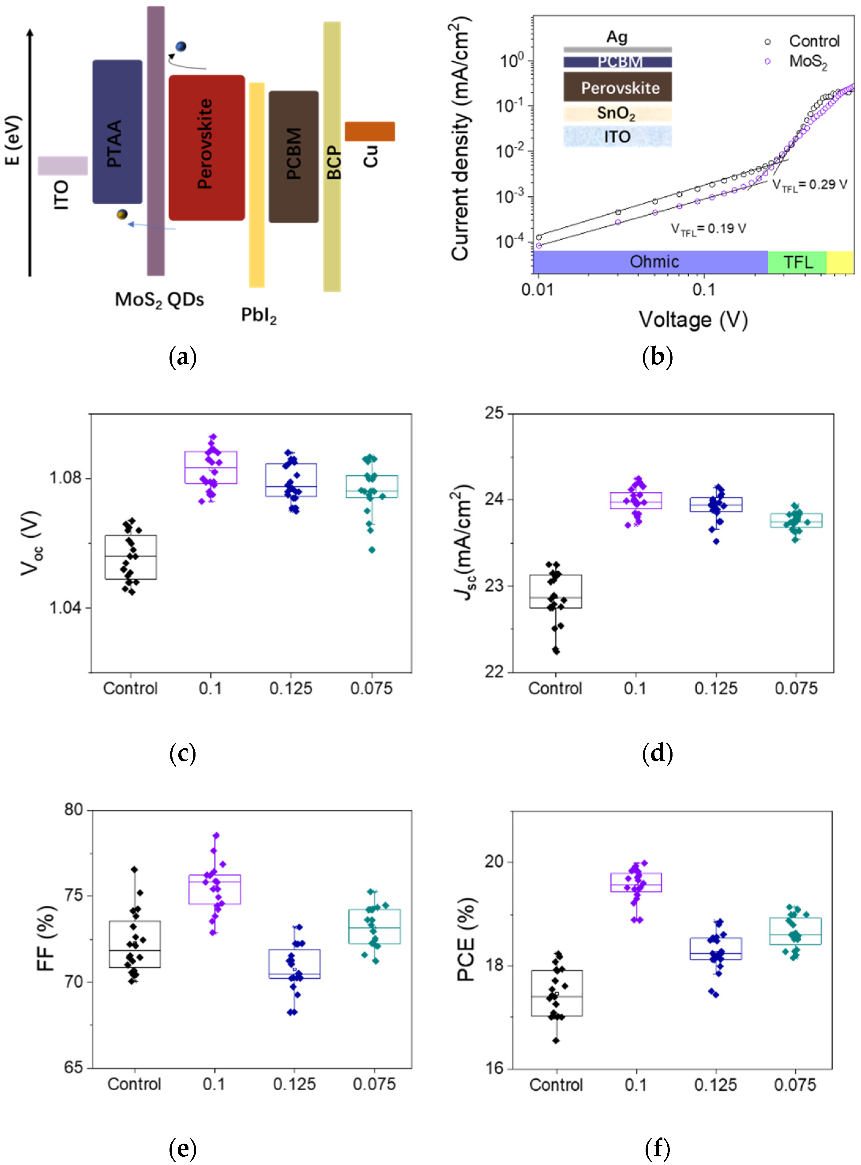
3. Results and Discussion

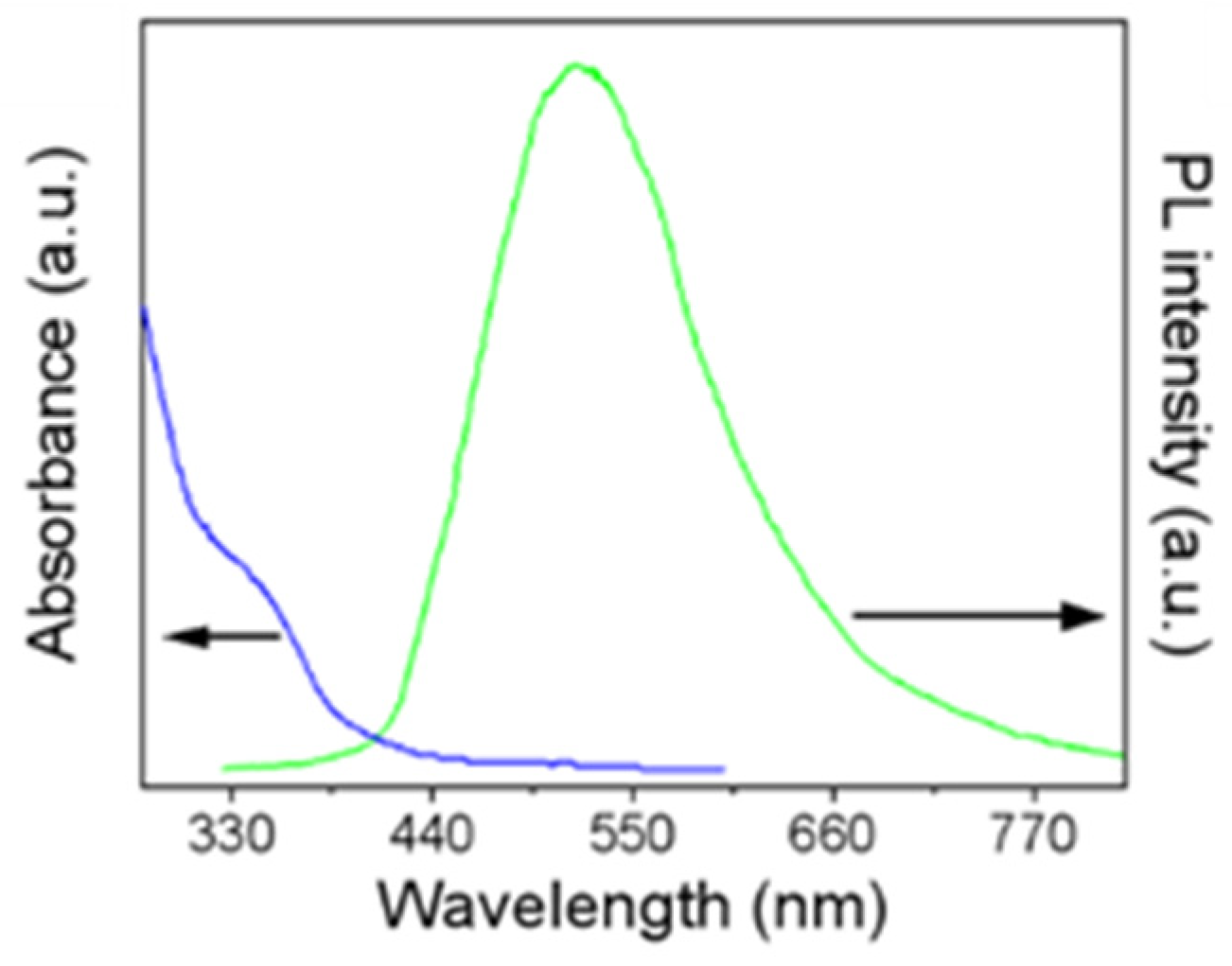
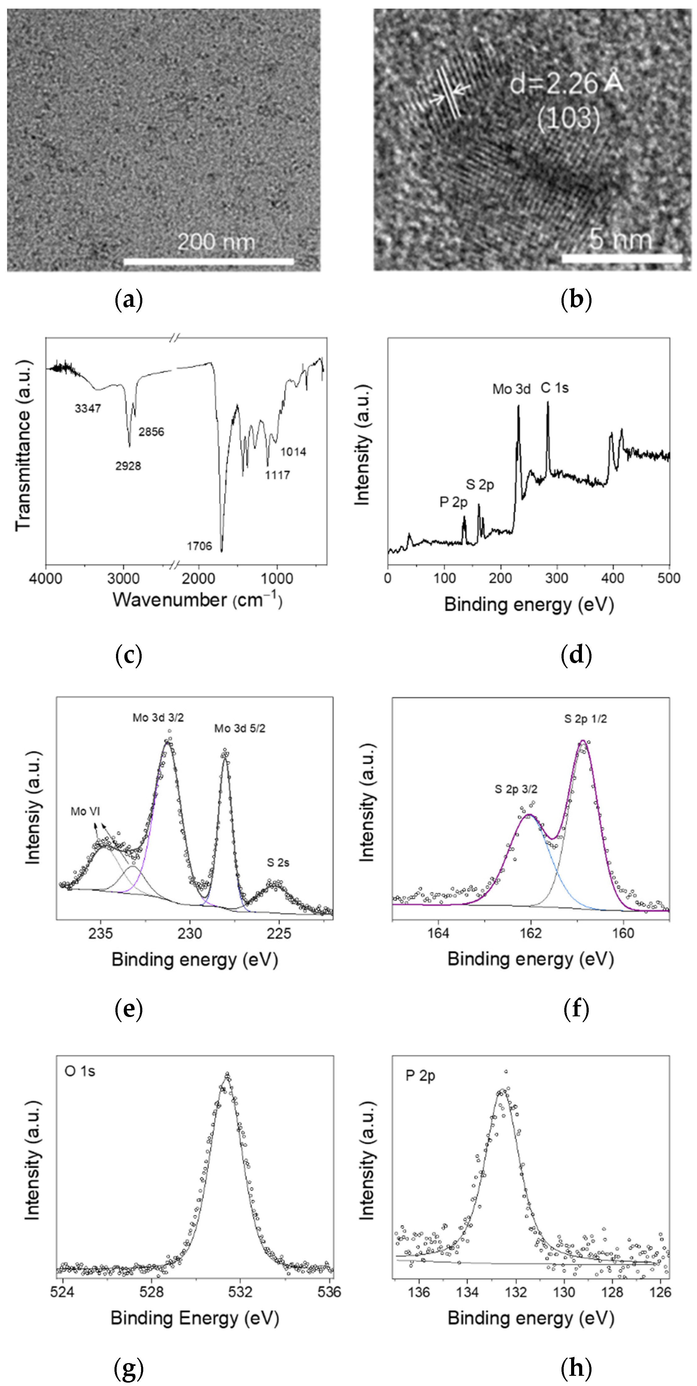
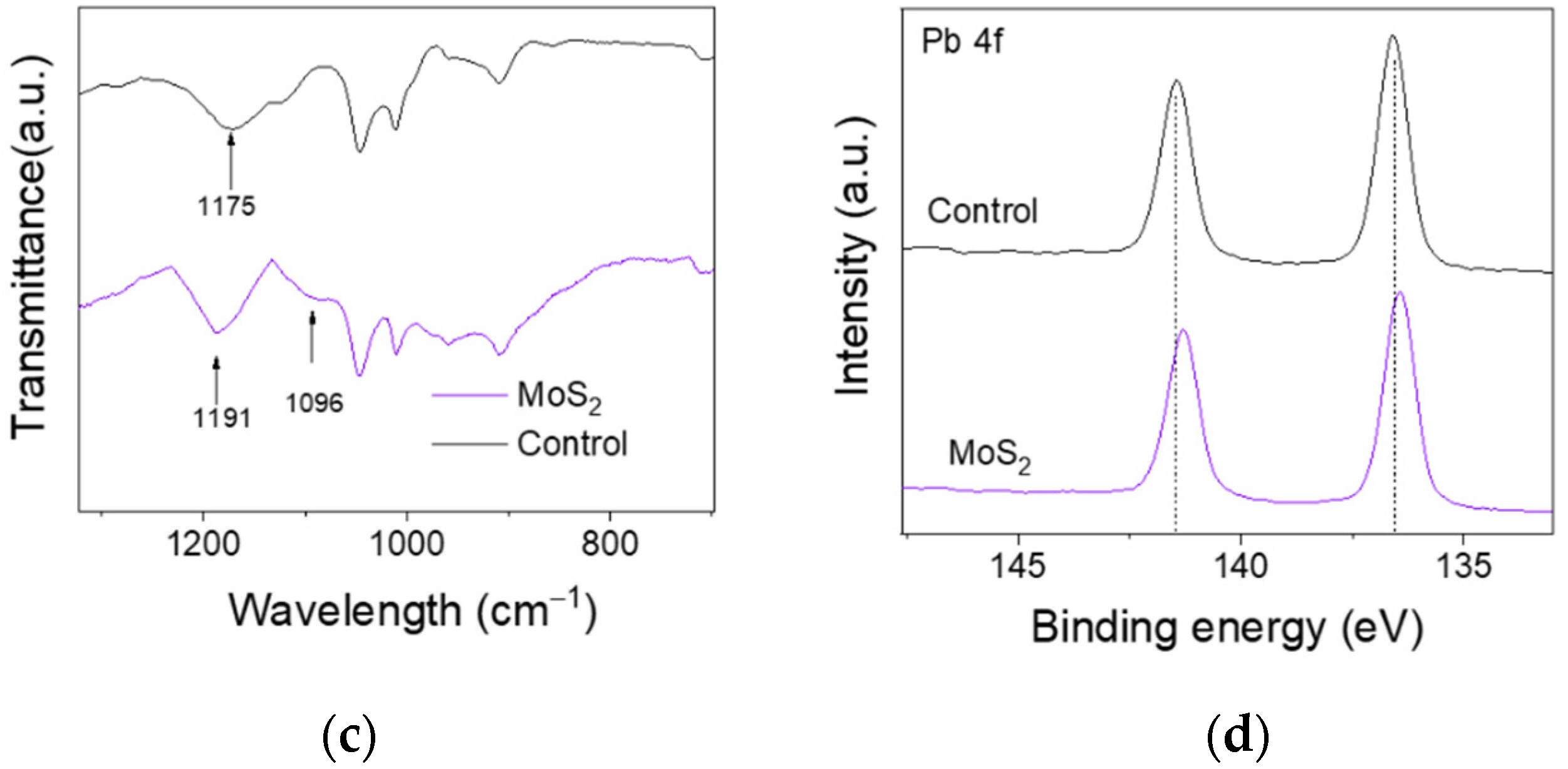
3.1. Characterization of MoS2 QDs

The MoS2 QDs were prepared hydrothermally, wherein the deionized water was replaced by NMP. Due to the strong stripping ability of NMP, the formation of bulk MoS2 can be suppressed during the synthesis [23]. Tri-n-octylphosphine (TOP) was oxidized to Tri-n-octylphosphine oxide, capping the MoS2 QDs and further restricting the size of the quantum dots.
A transmission electron microscopy (TEM) image is given as Figure 1a, showing the morphology of MoS2 QDs. The uniformly dispersed MoS2 QDs indicates their excellent polydispersity in DMF. The high-resolution TEM image (Figure 1b) shows the interplanar spacing of 2.26 Å of a near-spherical particle, which is assigned to the (103) plane of MoS2. The X-ray photoelectron spectroscopy (XPS) spectra were characterized to determine the chemical states and the element composition of the as-prepared MoS2 QDs. The peaks of Mo, S, P, and C are clearly observable in the survey spectrum (Figure 1c). Figure 1d shows characteristic peaks at 162.05 eV and 160.9 eV, which are relevant to S 2p 1/2 and S 2p 3/2 orbitals, respectively. Two strong peaks located at 228.05 eV and 231.35 eV in Figure 1e are assigned to Mo 3d 5/2 and Mo 3d 3/2 orbitals, respectively, proving the existence of Mo4+. There are two peaks at 234.8 and 235.95 eV assigned to Mo6+ 3d5/2 and Mo6+ 3d3/2. The higher valance resulted from the partial oxidation of MoS2 QD with the remaining oxygen in the Teflon-lined stainless-steel autoclave during the reaction [24,25]. Moreover, the atomic ratio of S to Mo is calculated as ~1.89. In addition, the P element from TOP can also be detected from the XPS, as shown in Figure 1g,h. The P 2p and the O 1s signal prove the formation of the oxidation product of TOP. As shown in the Fourier transform infrared (FTIR) spectrum of MoS2 QDs (Figure 1f), the four dominating peaks at 3347, 2928, 2856, and 1706 cm−1 can be observed, corresponding to NH2, CH2, CH3, and C=O groups, respectively. The peaks at 1117 and 1014 cm−1 are assigned to P=O [26,27], indicating that the oxidation product of TOP serves as the surface ligand of MoS2 QDs, which is in line with the XPS results.
Figure 2 shows the UV-visible absorption and photoluminescence (PL) spectra of MoS2 QDs. The PL peak and absorption peak are located at 518 nm and 343 nm, respectively. The band gap of MoS2 QDs can be calculated from the absorption spectrum according to Lambert–Beer’s law, which is described as:
(αhν)2 = BK2 (Eg)
where B and K are proportionality constants, α is the absorption coefficient, Eg is the band gap energy, and is the energy of incident photons. Based on the quantum confinement effect [28], the Eg of the as-prepared MoS2 QDs is about 2.68 eV.

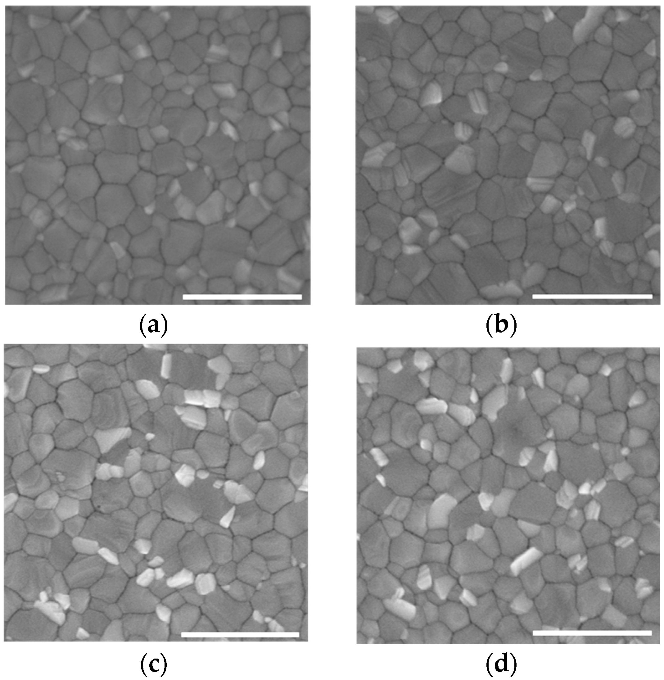
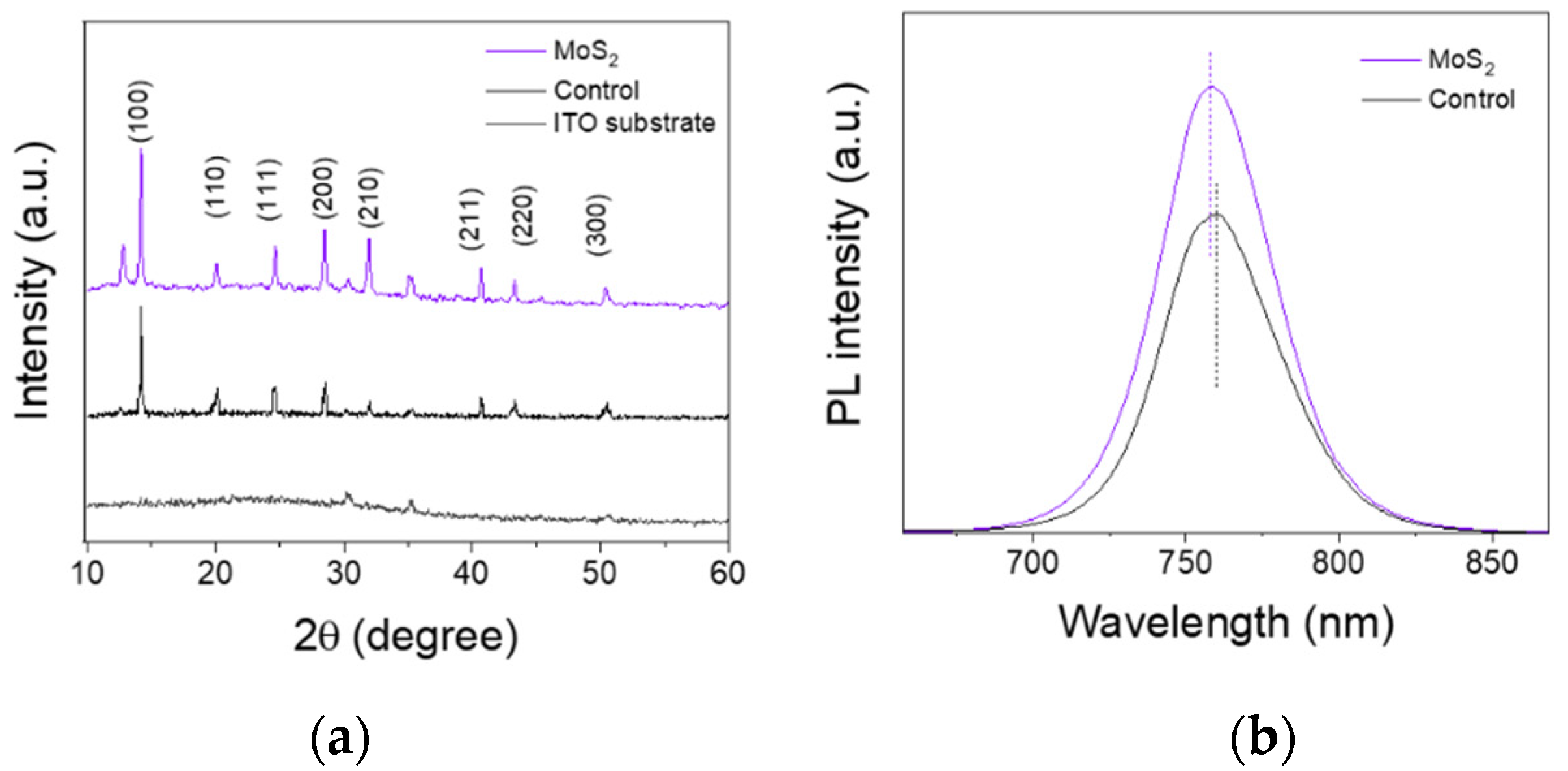
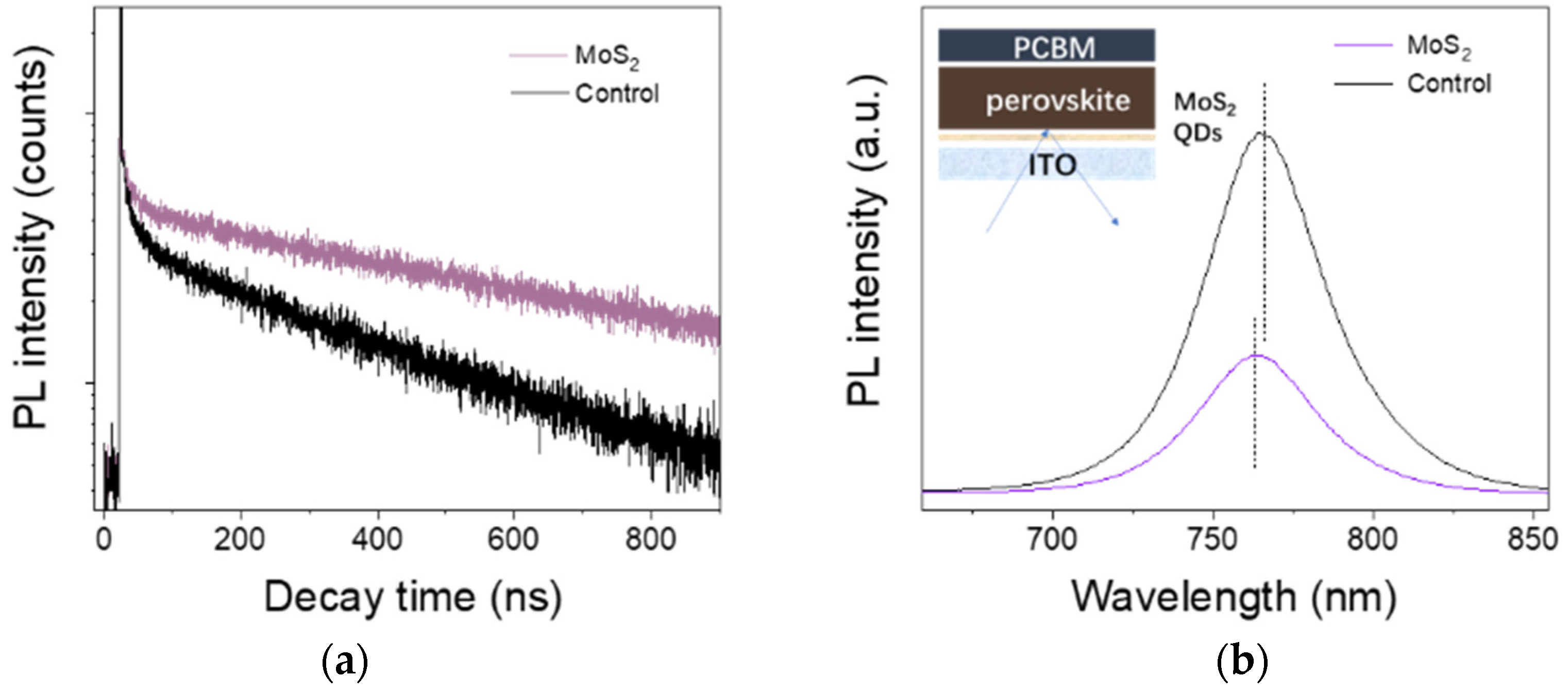
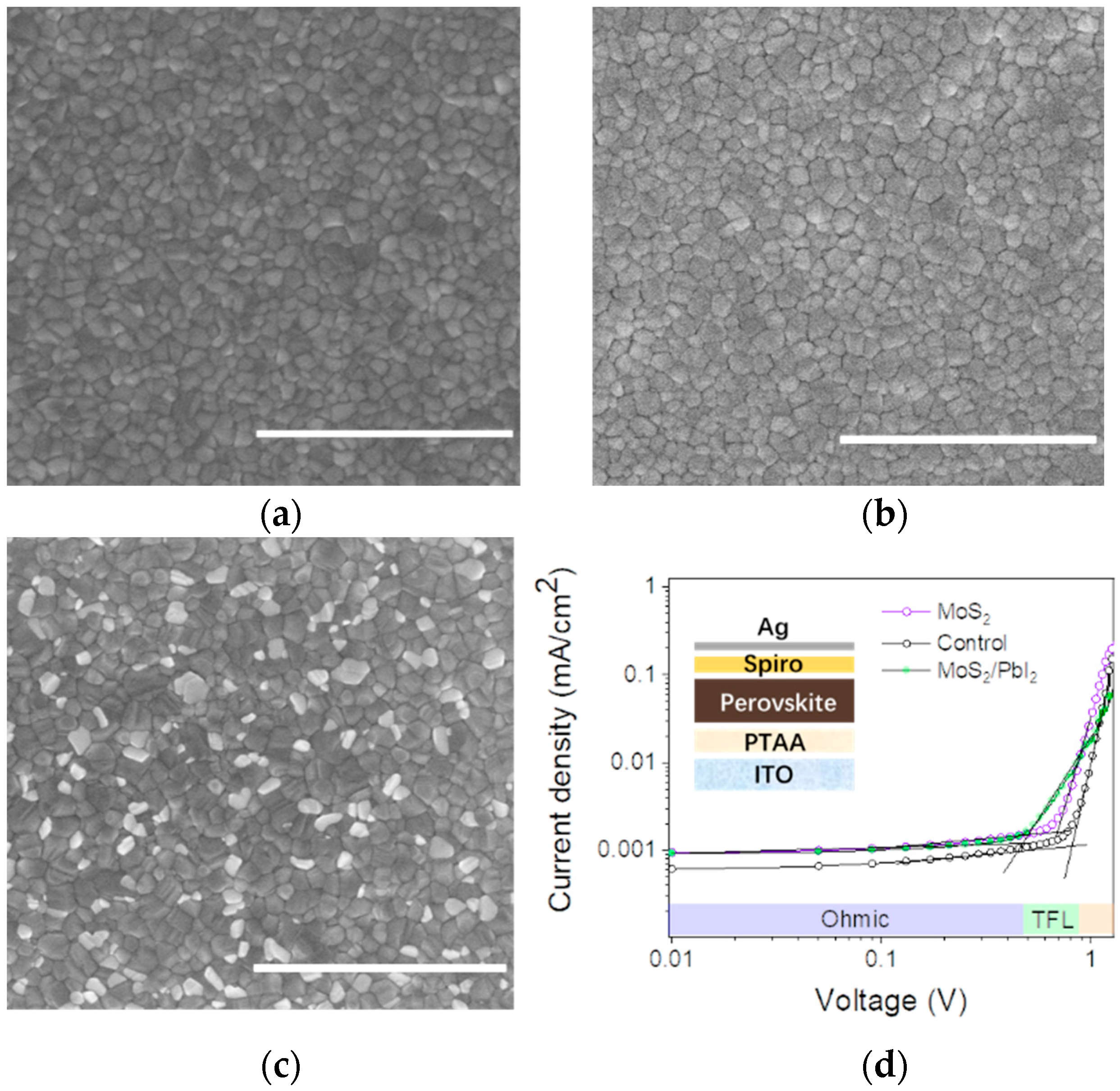
3.2. Characterization of Perovskite Films

To determine the influence of MoS2 QDs on perovskite films, the top-view SEM images shown in Figure 3 were compared. It was noted that the film with MoS2 QD modification exhibits more homogeneous grains, and some light-colored particles are distributed on top of the films, which can be observed as PbI2 by X-ray diffraction (XRD) patterns in Figure 4a [6].
The XRD patterns of the perovskite films deposited on the PTAA and PTAA/MoS2 QD substrate are shown in Figure 4a. The perovskite films both present characteristic diffraction peaks [29]. There are no perovskite peak position shifts, indicating that the Mo or S atom did not diffuse into the perovskite crystal and enable doping. Compared with the control film, the perovskite film deposited on the PTAA/MoS2 QD substrate suggests a peak at 12.5° belonging to (001) crystal planes of PbI2, which is consistent with the SEM analysis [30,31,32]. Moreover, the increased intensity of the peaks corresponding to perovskites evidently indicates a higher quality of perovskite films and crystal-oriented growth. The promoted peak intensity can be attributed to the interaction between MoS2 QDs and perovskites. MoS2 QDs served as a growth template and induced crystal growth [33]. The FTIR spectra of the perovskite film with MoS2 QDs and without are shown in Figure 4c. The peak shifts from 1175 to 1191 cm−1, which overlaps P=O peaks. Moreover, there is a new peak at 1096 cm−1 belonging to P=O. Compared to the QD FTIR spectrum, the peak shifts from 1014 cm−1 to 1096 cm−1.
To determine the chemical effects of MoS2 QD modification, the buried interfaces were characterized using XPS [6]. The XPS results of the MoS2-QD-modified perovskite and control film are shown in Figure 4d. According to the XPS spectra of the Pb 4f region, the binding energy decreased from 136.58 eV and 141.45 eV to 136.40 eV and 141.28 eV, respectively. The lower binding energy of Pb could be ascribed to the strong interaction between the QD modification and Pb through the Lewis acid–base interaction. The XPS results confirm the interaction between the MoS2 QD layer and perovskite films, indicating increased electron density [34]. The XPS results confirm the interaction between the MoS2 QD layer and perovskite films.
To further characterize the effects of MoS2 QDs on the photophysical properties of perovskites, we observed the steady-state PL spectra of the perovskite films with and without MoS2 QDs, as shown in Figure 4b. It is noted that the PL peak blue-shifts from 761 nm to 759 nm with the assistance of MoS2 QDs, indicating a lower density of trap states [35,36]. Meanwhile, the perovskite film with MoS2 QDs presents a much higher PL intensity, which means less nonradiative recombination losses [37]. Combined with the XPS results, the Pb 4f peaks shift toward the lower binding energy, demonstrating that the suppressed nonradiative recombination in the perovskite films is related to the interaction between the QDs and perovskites, which is responsible for the reduced traps and improved PL.
To evaluate the effects of MoS2 QDs on the carrier dynamics, time-resolved photoluminescence (TRPL) measurement was employed. As shown in Figure 5a, TRPL curves were fitted using a bi-exponential function described as:
I(t) = I0 + A1 exp(−t/τ1) + A2 exp(−t/τ2)
where τ1 and τ2 represent the fast decay time constant and the slow time constant, respectively, and A1 and A2 are the amplitudes of the fast and slow decay processes [38,39]. The average carrier lifetime (τave) was acquired through equation τave = τ1·f1+ τ1·f2.
The fitting relevant parameters are summarized in Table 1. The proportion of the fast decay component τ1 representing the surface trap-assisted nonradiative recombination decreased from 52% to 40.5%. Moreover, the prolonged average carrier lifetime (398.8 ns) compared with that of the control film (175.3 ns) further demonstrates the promoted photophysical properties of suppressing the nonradiative recombination processes.
We also noted the formation of PbI2 on the surface and at the grain boundaries. The PL peaks were compared to further understand the influence of PbI2 in Figure 5b. When the PCBM film as electron transport layer (ETL) was deposited on top of the perovskite films, the sample with QDs showed significantly weaker PL, demonstrating that carriers were extracted more efficiently the pure perovskite film. It is reported that the PbI2 located at the surface of the perovskite film could heal the halide vacancy forming type-I band alignment and reduce the trap state density [36,40,41,42,43].

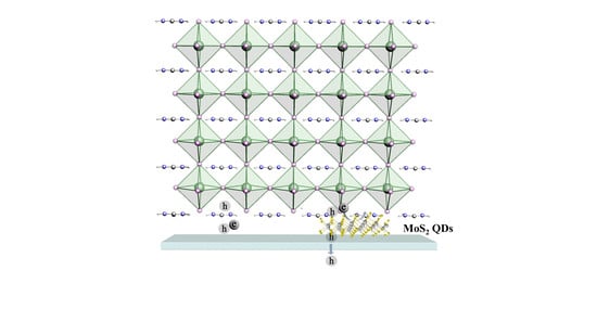
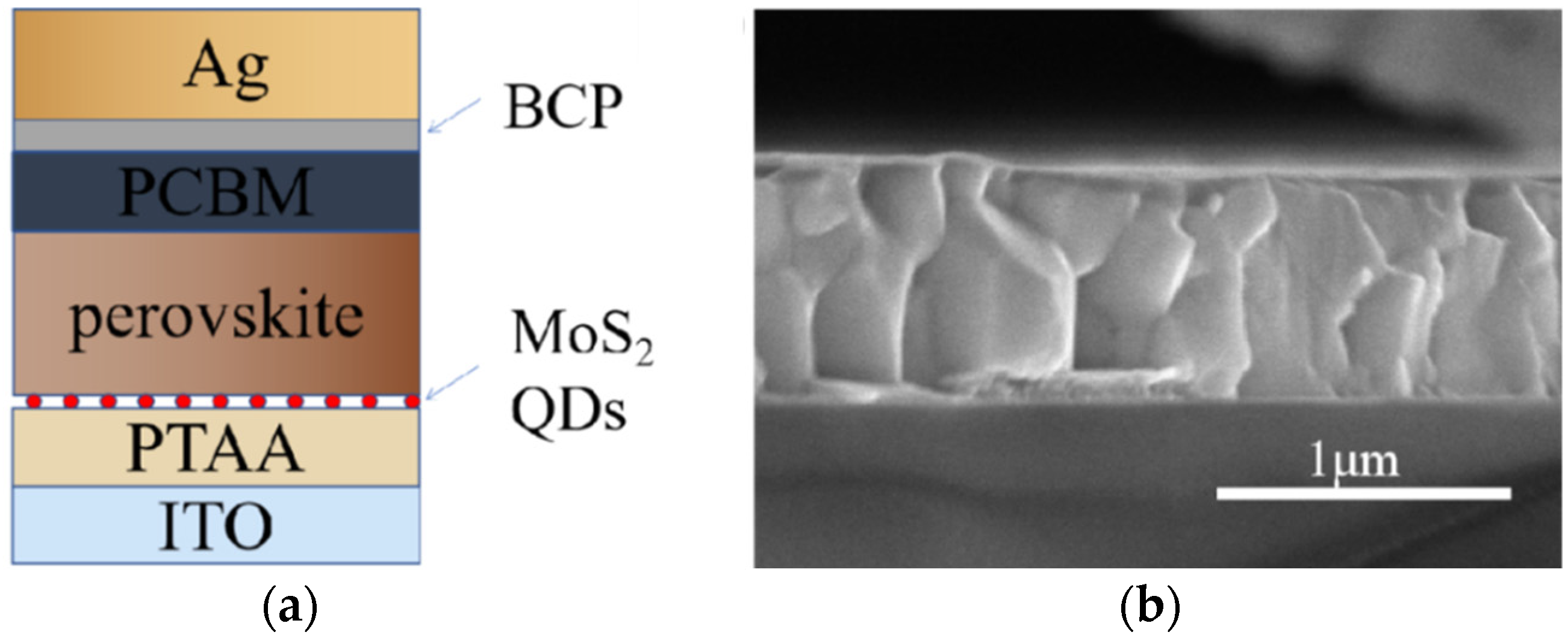
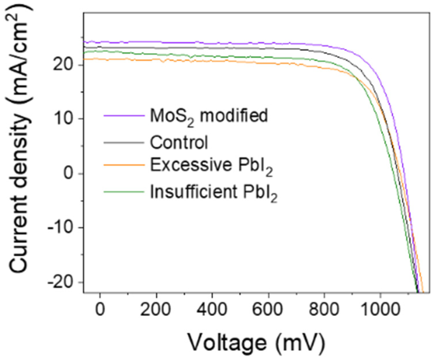
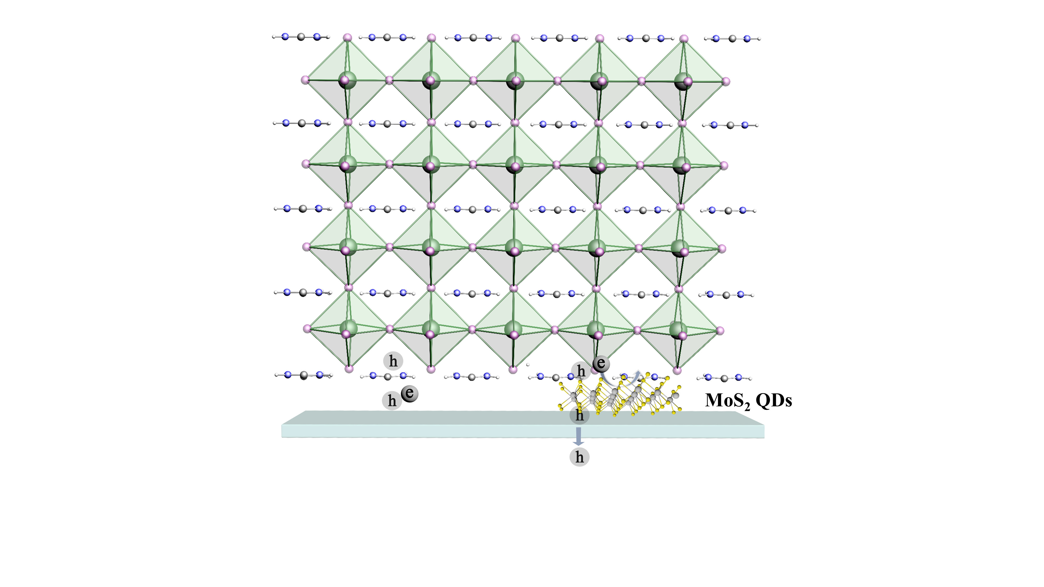
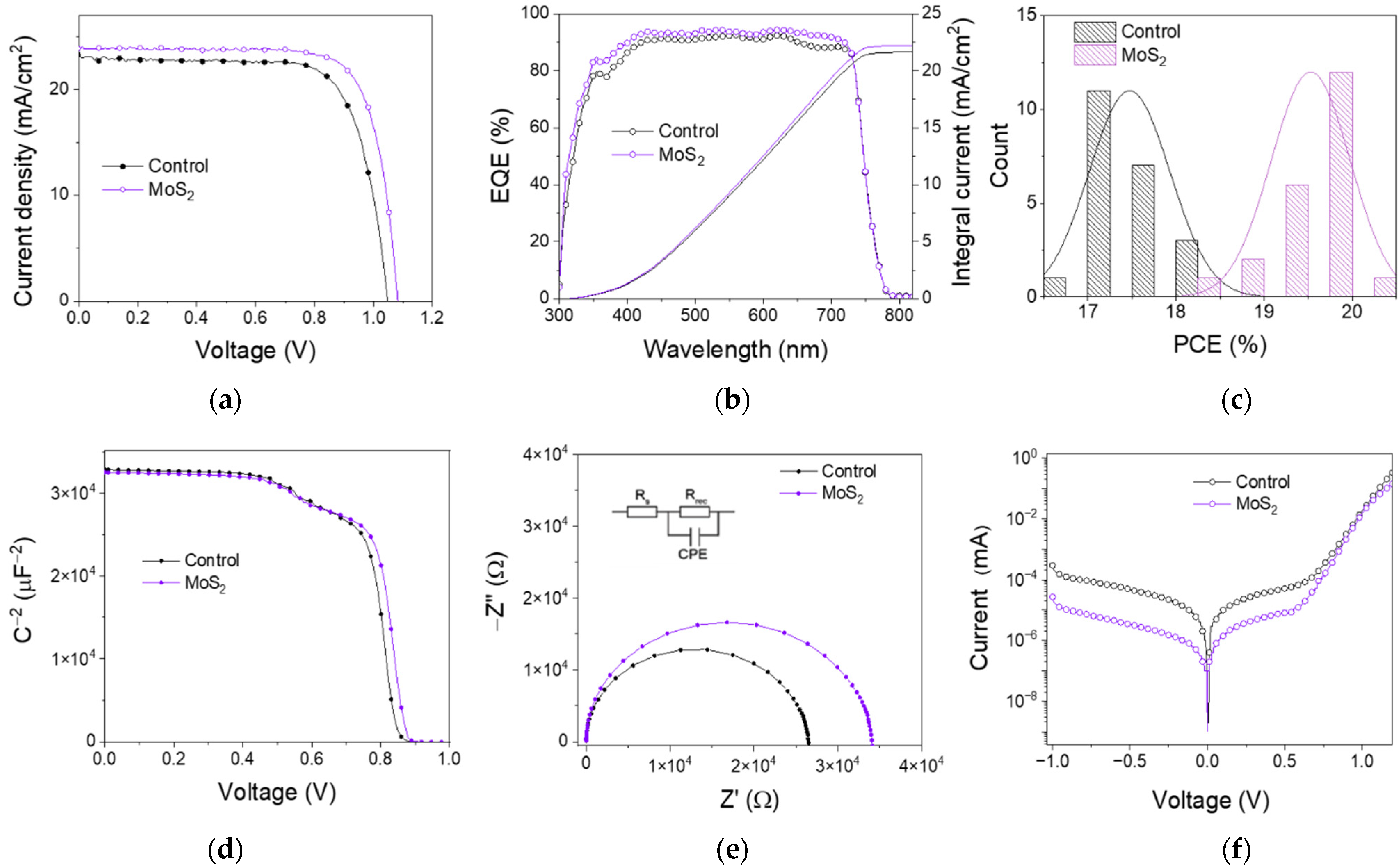
3.3. Perovskite Solar Cell Performances

Typical perovskite solar cells (PSCs) were fabricated with the structure of ITO/PTAA/perovskite/PCBM/BCP/Ag, as shown in Figure 6a. A cross-section SEM of the device is shown in Figure 6b.
The current density–voltage (J–V) curves of the devices are provided in Figure 7a, while the device parameters are summarized in Table 2. As expected, due to the QDs’ passivation effect, the Voc (open circuit voltage) and Jsc (short circuit current) were enhanced from 1.05 to 1.08 V and 23.25 mA/cm2 to 23.79 mA/cm2, respectively. Consequently, a relatively superior performance with a power convention efficiency (PCE) from 17.87% to 19.95% was achieved. Figure 7c shows the statistic efficiency distribution. The current densities integrated from the incident photon to converted electron spectra (IPCE) increased from 21.67 to 22.15 mA/cm2 with the MoS2 modification, which is consistent with the increased Jsc. The enhancement of IPCE (Figure 7b) in the short wavelength part could be attributed to the MoS2 QDs at the HTL interface acting as an interface passivator. Furthermore, the increase in long wavelength conversion may be related to the passivation effect of lead iodide at the electron collection side.
To further investigate the influence of MoS2 QD modification on the carrier extraction/transport in devices, dark capacitance–voltage curves were measured, as shown in Figure 7d. The Mott–Schottky relationship can be described as follows:
1/C2 = 2(VVbikT/e)/(εε0eND)
where Vbi is the voltage of the built-in electric field, V is the applied voltage, C is the capacitance, k is the Boltzmann’s constant, T represents the temperature, and ND is the donor density. The fitting results show that the Vbi of the device with MoS2 QDs increased from 0.84 V to 0.86 V. The enhanced driving force to separate photogenerated carriers accounts for the higher Voc [44,45].
Electrochemical impedance spectroscopy (EIS) under 0.85 V bias voltage and dark conditions was performed to further explore the charge transfer and recombination progress [1,46]. Nyquist plots of devices with and without MoS2 are presented in Figure 7e. An equivalent circuit model is depicted as an inset where series resistance (Rs) and recombination resistance (Rrec) represent the resistance corresponding to the behavior of carrier transport and recombination, respectively. The plot for devices with MoS2 QDs clearly shows a larger diameter of the semicircle than that of the control device, indicating a larger recombination resistance and chemical capacitance, which corroborates the suppression of carrier recombination and an improvement in transfer and extraction efficiency. This phenomenon can be ascribed to the passivation of the defects and band alignment at the interface. Dark JV curves were measured to confirm the buffer function of MoS2 QD modification. As shown in Figure 7f, current leakage of the device was reduced by nearly more than one order of magnitude with the introduction of MoS2 QDs. The remarkable decrease in the current leakage demonstrates that MoS2 QDs as a buffer layer prevent the photogenerated electrons from flowing to the hole transport layer [47,48,49].
To further individually clarify the effect of PbI2 and MoS2, we adopted the mechanical exfoliation method to remove the PbI2 on the top surface of the perovskite films [50]. The films without PbI2 SEM images are shown in Figure 8a–c. Based on the treated films, we fabricated hole-only devices with and without MoS2.
Subsequently, space-charge-limited current (SCLC) measurements were carried out to estimate the trap densities by employing hole-only device configurations (ITO/PTAA/Perovskite/Spiro-OMeTAD/Ag). According to the SCLC mode, the defect state density is determined by the following equation [51,52]:
nt = (2εε0VTFL)/(eL2)
where nt is trap density; VTFL represents trap-filled limited voltage; e is elementary charge; and ε and ε0 are the permittivity of perovskite films and the vacuum permittivity, respectively.
Figure 8d suggests that the VTFL for the optimized device is 0.70 V compared to the control device’s 0.81 V. Without PbI2, the defect density is reduced from 9.6 × 10¹⁵ to 8.3 × 10¹⁵, which could individually prove the MoS2 effects. The reduced trap density demonstrates that the introduction of MoS2 QDs can effectively suppress carrier recombination, which is consistent with the prolonged carrier lifetime and improved device performance. Furthermore, the films with MoS2 and PbI2 show the least defective state density, which is 6.9 × 10¹⁵. These results prove the synergistic passivation of MoS2 and PbI2.
Electron-only devices were fabricated, and the trap state density for electron transfer was calculated in Figure 9b. The defect state density decreased from 1.25 × 1016 cm−3 to 0.82 × 1016 cm−3. As shown in the schematic diagram of band energy (Figure 9a), the PbI2 on the electron transfer layer side could facilitate the extraction of electrons and reduce the defect state density. Thus, we assume that the MoS2 on the buried interface and the PbI2 on the top interface promote hole and electron transfer, respectively.
We introduced 5% excess PbI2 and reduce the 5% proportion PbI2 in the precursor on the base of the component proportion in the manuscript and then respectively fabricated devices, namely excessive PbI2 and insufficient PbI2. The devices with 5% excessive PbI2, insufficient PbI2 and control device performances are compared in the Figure 10.
The device parameters are shown in Table 3. The device introduced to 5% excess PbI2 in the precursor showed significant current density decline, while the device with excessive PbI2 showed enhanced open voltage compared to the other devices. The con-trol device suggests higher current density compared to the insufficient device and ex-cess device, which indicates that a proportion of the control devices are best without modification.
Based on the above experiment and analysis, a conclusion could be drawn: the MoS2 QDs could passivate the defect through the interaction without PbI2, while the PbI2 induced by MoS2 reduced the trap density further. Simply adding excessive PbI2 could not achieve higher efficiency and lower trap density. The box plot statistics of Voc, Jsc, FF, and PCEs of 20 devices for each fabrication condition are shown in Figure 9c–f. The MoS2-modified device without PbI2 showed lower defect density. In a word, the PbI2 induced by MoS2 QDs and MoS2 both play a role in passivation. Under synergistic effects, the current density and open voltage were both improved.

4. Conclusions

In summary, we employed MoS2 QDs as interface passivating agents to improve the performance of perovskite solar cells. It was found that MoS2 QDs can improve perovskite crystallinity and passivate interfacial defects, which prolongs carrier lifetimes and suppresses carrier recombination. Moreover, due to the wide bandgap of 2.6 eV, the MoS2 QDs served as a buffer layer, reducing the shunting paths. Benefitting from the suppressed nonradiative recombination and reduced leakage current, the device performance of PSCs improved from 17.87% to 19.95% after MoS2 QD modification. This work provides an exploration of QDs for PSC applications, specifically for perovskite film modification and buried interface passivation.

Author Contributions

Conceptualization, W.Z. (Wei Zhang) and X.Z.; Data curation, Z.L., T.G., C.W. and W.D.; Formal analysis, Z.L., T.G. and J.Z.; Funding acquisition, X.Z. and W.Z. (Weitao Zheng); Investigation, Z.L., T.G., J.L., W.Z. (Wei Zhang) and X.Z.; Methodology, Z.L., C.W. and W.D.; Project administration, X.Z. and W.Z. (Weitao Zheng); Resources, X.Z. and W.Z. (Weitao Zheng); Software, J.W. and W.D.; Supervision, W.Z. (Wei Zhang) and X.Z.; Validation, T.G., C.W. and W.Z. (Weitao Zheng); Visualization, J.W.; Writing—original draft, Z.L. and T.G. All authors have read and agreed to the published version of the manuscript.

Funding

This research was funded by National Natural Science Foundation of China (51972136 and 52072141), Interdisciplinary Integration and Innovation Project of JLU (JLUXKJC2021QZ12), and Fundamental Research Funds for the Central Universities (JLU, 1018320194002, 2019JCXK-31, S202110183229).

Data Availability Statement

The data that support the findings of this study are available from the corresponding author upon reasonable request.

Conflicts of Interest

The authors declare no conflict of interest.

References

  1. Yang, Z.; Yu, Z.; Wei, H.; Xiao, X.; Ni, Z.; Chen, B.; Deng, Y.; Habisreutinger, S.N.; Chen, X.; Wang, K.; et al. Enhancing Electron Diffusion Length in Narrow-Bandgap Perovskites for Efficient Monolithic Perovskite Tandem Solar Cells. Nat. Commun. 2019, 10, 4498. [Google Scholar] [CrossRef] [PubMed]
  2. Kumar, N.; Lee, H.B.; Hwang, S.; Kang, J.W. Large-Area, Green Solvent Spray Deposited Nickel Oxide Films for Scalable Fabrication of Triple-Cation Perovskite Solar Cells. J. Mater. Chem. A 2020, 8, 3357–3368. [Google Scholar] [CrossRef]
  3. Sandhu, S.; Saharan, C.; Buruga, S.K.; Kumar, S.A.; Rana, P.S.; Nagajyothi, P.C.; Mane, S.D. Micro Structurally Engineered Hysteresis-Free High Efficiency Perovskite Solar Cell Using Zr-Doped Tio2 Electron Transport Layer. Ceram. Int. 2021, 47, 14665–14672. [Google Scholar] [CrossRef]
  4. Shao, Y.; Yuan, Y.; Huang, J. Correlation of Energy Disorder and Open-Circuit Voltage in Hybrid Perovskite Solar Cells. Nat. Energy 2016, 1, 15001. [Google Scholar] [CrossRef]
  5. Chen, S.; Dai, X.; Xu, S.; Jiao, H.; Zhao, L.; Huang, J. Stabilizing Perovskite-Substrate Interfaces for High-Performance Perovskite Modules. Science 2021, 373, 902–907. [Google Scholar] [CrossRef] [PubMed]
  6. Yang, X.; Luo, D.; Xiang, Y.; Zhao, L.; Anaya, M.; Shen, Y.; Wu, J.; Yang, W.; Chiang, Y.H.; Tu, Y.; et al. Buried Interfaces in Halide Perovskite Photovoltaics. Adv. Mater. 2021, 33, e2006435. [Google Scholar] [CrossRef]
  7. Dong, W.; Zhang, X.; Yang, F.; Zeng, Q.; Yin, W.; Zhang, W.; Wang, H.; Yang, X.; Kershaw, S.V.; Yang, B.; et al. Amine-Terminated Carbon Dots Linking Hole Transport Layer and Vertically Oriented Quasi-2d Perovskites through Hydrogen Bonds Enable Efficient Leds. ACS Nano 2022, 16, 9679–9690. [Google Scholar] [CrossRef]
  8. Kim, K.M.; Ahn, S.; Jang, W.; Park, S.; Park, O.O.; Wang, D.H. Work Function Optimization of Vacuum Free Top-Electrode by Pedot:Pss/Pei Interaction for Efficient Semi-Transparent Perovskite Solar Cells. Sol. Energy Mater. Sol. Cells 2018, 176, 435–440. [Google Scholar] [CrossRef]
  9. Jia, X.; Wu, N.; Wei, J.; Zhang, L.; Luo, Q.; Bao, Z.; Li, Y.-Q.; Yang, Y.; Liu, X.; Ma, C.-Q. A Low-Cost and Low-Temperature Processable Zinc Oxide-Polyethylenimine (Zno:Pei) Nano-Composite as Cathode Buffer Layer for Organic and Perovskite Solar Cells. Org. Electron. 2016, 38, 150–157. [Google Scholar] [CrossRef]
  10. Zhang, X.; Lin, H.; Huang, H.; Reckmeier, C.; Zhang, Y.; Choy, W.C.; Rogach, A.L. Enhancing the Brightness of Cesium Lead Halide Perovskite Nanocrystal Based Green Light-Emitting Devices through the Interface Engineering with Perfluorinated Ionomer. Nano Lett. 2016, 16, 1415–1420. [Google Scholar] [CrossRef]
  11. Degani, M.; An, Q.; Albaladejo-Siguan, M.; Hofstetter, Y.J.; Cho, C.; Paulus, F.; Grancini, G.; Vaynzof, Y. 23.7% Efficient Inverted Perovskite Solar Cells by Dual Interfacial Modification. Sci. Adv. 2021, 7, eabj7930. [Google Scholar] [CrossRef] [PubMed]
  12. Zhang, X.; Sun, C.; Zhang, Y.; Wu, H.; Ji, C.; Chuai, Y.; Wang, P.; Wen, S.; Zhang, C.; Yu, W.W. Bright Perovskite Nanocrystal Films for Efficient Light-Emitting Devices. J. Phys. Chem. Lett. 2016, 7, 4602–4610. [Google Scholar] [CrossRef] [PubMed]
  13. Shao, S.; Abdu-Aguye, M.; Qiu, L.; Lai, L.-H.; Liu, J.; Adjokatse, S.; Jahani, F.; Kamminga, M.E.; Brink, G.H.T.; Palstra, T.T.M.; et al. Elimination of the Light Soaking Effect and Performance Enhancement in Perovskite Solar Cells Using a Fullerene Derivative. Energy Environ. Sci. 2016, 9, 2444–2452. [Google Scholar] [CrossRef]
  14. Wang, Y.; Wu, T.; Barbaud, J.; Kong, W.; Cui, D.; Chen, H.; Yang, X.; Han, L. Stabilizing Heterostructures of Soft Perovskite Semiconductors. Science 2019, 365, 687–691. [Google Scholar] [CrossRef]
  15. Litvin, A.P.; Zhang, X.; Ushakova, E.V.; Rogach, A.L. Carbon Nanoparticles as Versatile Auxiliary Components of Perovskite-Based Optoelectronic Devices. Adv. Funct. Mater. 2021, 31, 2010768. [Google Scholar] [CrossRef]
  16. Zhang, X.; Zeng, Q.; Xiong, Y.; Ji, T.; Wang, C.; Shen, X.; Lu, M.; Wang, H.; Wen, S.; Zhang, Y.; et al. Energy Level Modification with Carbon Dot Interlayers Enables Efficient Perovskite Solar Cells and Quantum Dot Based Light-Emitting Diodes. Adv. Funct. Mater. 2020, 30, 1910530. [Google Scholar] [CrossRef]
  17. Zheng, X.; Troughton, J.; Gasparini, N.; Lin, Y.; Wei, M.; Hou, Y.; Liu, J.; Song, K.; Chen, Z.; Yang, C.; et al. Quantum Dots Supply Bulk- and Surface-Passivation Agents for Efficient and Stable Perovskite Solar Cells. Joule 2019, 3, 1963–1976. [Google Scholar] [CrossRef]
  18. Tang, G.; You, P.; Tai, Q.; Yang, A.; Cao, J.; Zheng, F.; Zhou, Z.; Zhao, J.; Chan, P.K.L.; Yan, F. Solution-Phase Epitaxial Growth of Perovskite Films on 2d Material Flakes for High-Performance Solar Cells. Adv. Mater. 2019, 31, e1807689. [Google Scholar] [CrossRef]
  19. Hu, W.; Jin, X.; Li, A.; Liu, C.L.; Wang, X.F. Efficiency Improvement of Inverted Perovskite Solar Cells Enabled by Ptaa/Mos2 Double Hole Transporters. Nanotechnology 2022, 33, 335202. [Google Scholar] [CrossRef]
  20. Capasso, A.; Matteocci, F.; Najafi, L.; Prato, M.; Buha, J.; Cinà, L.; Pellegrini, V.; di Carlo, A.; Bonaccorso, F. Few-Layer Mos2flakes as Active Buffer Layer for Stable Perovskite Solar Cells. Adv. Energy Mater. 2016, 6, 1600920. [Google Scholar] [CrossRef]
  21. Kakavelakis, G.; Paradisanos, I.; Paci, B.; Generosi, A.; Papachatzakis, M.; Maksudov, T.; Najafi, L.; Del Rio Castillo, A.E.; Kioseoglou, G.; Stratakis, E.; et al. Extending the Continuous Operating Lifetime of Perovskite Solar Cells with a Molybdenum Disulfide Hole Extraction Interlayer. Adv. Energy Mater. 2018, 8, 1702287. [Google Scholar] [CrossRef]
  22. Najafi, L.; Taheri, B.; Martin-Garcia, B.; Bellani, S.; di Girolamo, D.; Agresti, A.; Oropesa-Nunez, R.; Pescetelli, S.; Vesce, L.; Calabro, E.; et al. Mos2 Quantum Dot/Graphene Hybrids for Advanced Interface Engineering of a Ch3nh3pbi3 Perovskite Solar Cell with an Efficiency of over 20. ACS Nano 2018, 12, 10736–10754. [Google Scholar] [CrossRef] [PubMed]
  23. Jawaid, A.; Nepal, D.; Park, K.; Jespersen, M.; Qualley, A.; Mirau, P.; Drummy, L.F.; Vaia, R.A. Mechanism for Liquid Phase Exfoliation of Mos2. Chem. Mater. 2016, 28, 337–348. [Google Scholar] [CrossRef]
  24. Zhu, X.; Xiang, J.; Li, J.; Feng, C.; Liu, P.; Xiang, B. Tunable Photoluminescence of Mos2 Quantum Dots Passivated by Different Functional Groups. J. Colloid Interface Sci. 2018, 511, 209–214. [Google Scholar] [CrossRef] [PubMed]
  25. Chen, J.; Li, S.; Ma, T.; Wu, D.; Zhao, Y.; Wang, C.; Zhao, D.; Li, X. Managing Lead Leakage in Efficient Perovskite Solar Cells with Phosphate Interlayers. Adv. Mater. Interfaces 2022, 9, 2200570. [Google Scholar] [CrossRef]
  26. Lu, X.; Korgel, A.B.A.; Johnston, K.P. High Yield of Germanium Nanocrystals Synthesized from Germanium Diiodide in Solution. Chem. Mater. 2005, 17, 6479–6485. [Google Scholar] [CrossRef]
  27. Chen, S.T.; Zhang, X.L.; Zhang, Q.H.; Tan, W.H. Trioctylphosphine as Both Solvent and Stabilizer to Synthesize Cds Nanorods. Nanoscale Res. Lett. 2009, 4, 1159–1165. [Google Scholar] [CrossRef]
  28. Dong, H.F.; Tang, S.S.; Hao, Y.S.; Yu, H.Z.; Dai, W.H.; Zhao, G.F.; Cao, Y.; Lu, H.T.; Zhang, X.J.; Ju, H.X. Fluorescent Mos2 Quantum Dots: Ultrasonic Preparation, up-Conversion and Down-Conversion Bioimaging, and Photodynamic Therapy. ACS Appl. Mater. Interfaces 2016, 8, 3107–3114. [Google Scholar] [CrossRef]
  29. Sadhu, A.; Rai, M.; Salim, T.; Jin, X.; Tan, J.M.R.; Leow, S.W.; Ahmed, M.G.; Magdassi, S.; Mhaisalkar, S.G.; Wong, L.H. Dual Role of Cu-Chalcogenide as Hole-Transporting Layer and Interface Passivator for P–I–N Architecture Perovskite Solar Cell. Adv. Funct. Mater. 2021, 31, 2103807. [Google Scholar] [CrossRef]
  30. Zhu, H.; Liu, Y.; Eickemeyer, F.T.; Pan, L.; Ren, D.; Ruiz-Preciado, M.A.; Carlsen, B.; Yang, B.; Dong, X.; Wang, Z.; et al. Tailored Amphiphilic Molecular Mitigators for Stable Perovskite Solar Cells with 23.5% Efficiency. Adv. Mater. 2020, 32, 1907757. [Google Scholar] [CrossRef]
  31. Jiang, X.; Zhang, J.; Ahmad, S.; Tu, D.; Liu, X.; Jia, G.; Guo, X.; Li, C. Dion-Jacobson 2d-3d Perovskite Solar Cells with Improved Efficiency and Stability. Nano Energy 2020, 75, 104892. [Google Scholar] [CrossRef]
  32. Luo, C.; Zhao, Y.; Wang, X.; Gao, F.; Zhao, Q. Self-Induced Type-I Band Alignment at Surface Grain Boundaries for Highly Efficient and Stable Perovskite Solar Cells. Adv. Mater. 2021, 33, e2103231. [Google Scholar] [CrossRef] [PubMed]
  33. Zheng, X.; Hou, Y.; Bao, C.; Yin, J.; Yuan, F.; Huang, Z.; Song, K.; Liu, J.; Troughton, J.; Gasparini, N.; et al. Managing Grains and Interfaces Via Ligand Anchoring Enables 22.3%-Efficiency Inverted Perovskite Solar Cells. Nat. Energy 2020, 5, 131–140. [Google Scholar] [CrossRef]
  34. Leng, X.; Wan, K.; Wang, H.; Wu, G.; Zhang, X.; Liu, Y.; Han, B.; Wang, B.; Zhang, Y.; Zhou, H.; et al. Adenosine Triphosphate Disodium Modified Hole Transport Layer for Efficient Inverted Perovskite Solar Cells. ChemNanoMat 2022, 8, e202200041. [Google Scholar] [CrossRef]
  35. Shao, Y.; Xiao, Z.; Bi, C.; Yuan, Y.; Huang, J. Origin and Elimination of Photocurrent Hysteresis by Fullerene Passivation in Ch3nh3pbi3 Planar Heterojunction Solar Cells. Nat. Commun. 2014, 5, 5784. [Google Scholar] [CrossRef]
  36. Jiang, X.; Zhang, J.; Liu, X.; Wang, Z.; Guo, X.; Li, C. Deeper Insight into the Role of Organic Ammonium Cations in Reducing Surface Defects of the Perovskite Film. Angew. Chem. 2022, 134, e202115663. [Google Scholar]
  37. Liu, X.; Zhang, Y.; Shi, L.; Liu, Z.; Huang, J.; Yun, J.S.; Zeng, Y.; Pu, A.; Sun, K.; Hameiri, Z.; et al. Exploring Inorganic Binary Alkaline Halide to Passivate Defects in Low-Temperature-Processed Planar-Structure Hybrid Perovskite Solar Cells. Adv. Energy Mater. 2018, 8, 1800138. [Google Scholar] [CrossRef]
  38. Chen, J.; Zhao, X.; Kim, S.; Park, N. Multifunctional Chemical Linker Imidazoleacetic Acid Hydrochloride for 21% Efficient and Stable Planar Perovskite Solar Cells. Adv. Mater. 2019, 31, 1902902. [Google Scholar] [CrossRef]
  39. Wu, Z.; Jiang, M.; Liu, Z.; Jamshaid, A.; Ono, L.K.; Qi, Y. Highly Efficient Perovskite Solar Cells Enabled by Multiple Ligand Passivation. Adv. Energy Mater. 2020, 10, 1903696. [Google Scholar] [CrossRef]
  40. Chen, Q.; Zhou, H.; Song, T.-B.; Luo, S.; Hong, Z.; Duan, H.-S.; Dou, L.; Liu, Y.; Yang, Y. Controllable Self-Induced Passivation of Hybrid Lead Iodide Perovskites toward High Performance Solar Cells. Nano Lett. 2014, 14, 4158–4163. [Google Scholar] [CrossRef]
  41. Wang, L.; McCleese, C.; Kovalsky, A.; Zhao, Y.; Burda, C. Femtosecond Time-Resolved Transient Absorption Spectroscopy of Ch3nh3pbi3 Perovskite Films: Evidence for Passivation Effect of Pbi2. J. Am. Chem. Soc. 2014, 136, 12205–12208. [Google Scholar] [CrossRef] [PubMed]
  42. Jiang, Q.; Chu, Z.; Wang, P.; Yang, X.; Liu, H.; Wang, Y.; Yin, Z.; Wu, J.; Zhang, X.; You, J. Planar-Structure Perovskite Solar Cells with Efficiency Beyond 21%. Adv. Mater. 2017, 29, 1703852. [Google Scholar] [CrossRef] [PubMed]
  43. Li, Y.; Li, W.; Xu, Y.; Li, R.; Yu, T.; Lin, Q. Interfacial Engineering of Perovskite Solar Cells with Evaporated Pbi2 Ultrathin Layers. ACS Appl. Mater. Interfaces 2021, 13, 53282–53288. [Google Scholar] [CrossRef] [PubMed]
  44. Zhang, F.; Guang, S.; Ye, M.; Xu, K.; Guo, W.; Liu, X.Y.; Xu, H. Chemical Decoration of Perovskites by Nickel Oxide Doping for Efficient and Stable Perovskite Solar Cells. ACS Appl. Mater. Interfaces 2018, 10, 36841–36850. [Google Scholar] [CrossRef]
  45. Wang, L.; Yan, Z.; Qiu, J.; Wu, J.; Zhen, C.; Tai, K.; Jiang, X.; Yang, S. Interface Regulation Enables Hysteresis Free Wide-Bandgap Perovskite Solar Cells with Low Voc Deficit and High Stability. Nano Energy 2021, 90, 106537. [Google Scholar] [CrossRef]
  46. Cao, Q.; Li, Y.; Zhang, H.; Yang, J.; Han, J.; Xu, T.; Wang, S.; Wang, Z.; Gao, B.; Zhao, J.; et al. Efficient and Stable Inverted Perovskite Solar Cells with Very High Fill Factors Via Incorporation of Star-Shaped Polymer. Science 2021, 7, eabg0633. [Google Scholar] [CrossRef]
  47. Duan, J.; Zhao, Y.; Yang, X.; Wang, Y.; He, B.; Tang, Q. Lanthanide Ions Doped Cspbbr3 Halides for Htm-Free 10.14%-Efficiency Inorganic Perovskite Solar Cell with an Ultrahigh Open-Circuit Voltage of 1.594 V. Adv. Energy Mater. 2018, 8, 1802346. [Google Scholar] [CrossRef]
  48. Zhang, J.; Liang, W.S.; Yu, W.; Yu, S.W.; Wu, Y.L.; Guo, X.; Liu, S.Z.; Li, C. A Two-Stage Annealing Strategy for Crystallization Control of Ch3nh3pbi3 Films toward Highly Reproducible Perovskite Solar Cells. Small 2018, 14, 1800181. [Google Scholar] [CrossRef]
  49. Sandhu, S.; Singh, R.; Yoo, K.; Kumar, M.; Lee, J.-J. Effect of Binary Additives in Mixed 2d/3d Sn-Based Perovskite Solar Cells. J. Power Sources 2021, 491, 229574. [Google Scholar] [CrossRef]
  50. Chen, S.; Liu, Y.; Xiao, X.; Yu, Z.; Deng, Y.; Dai, X.; Ni, Z.; Huang, J. Identifying the Soft Nature of Defective Perovskite Surface Layer and Its Removal Using a Facile Mechanical Approach. Joule 2020, 12, 2661–2674. [Google Scholar] [CrossRef]
  51. Qi, X.; Wang, J.; Tan, F.; Dong, C.; Liu, K.; Li, X.; Zhang, L.; Wu, H.; Wang, H.-L.; Qu, S.; et al. Quantum Dot Interface-Mediated Cspbibr2 Film Growth and Passivation for Efficient Carbon-Based Solar Cells. ACS Appl. Mater. Interfaces 2021, 13, 55338–55346. [Google Scholar] [CrossRef] [PubMed]
  52. Cai, Y.; Zhang, Z.; Zhou, Y.; Liu, H.; Qin, Q.; Lu, X.; Gao, X.; Shui, L.; Wu, S.; Liu, J. Enhancing the Efficiency of Low-Temperature Planar Perovskite Solar Cells by Modifying the Interface between Perovskite and Hole Transport Layer with Polymers. Electrochim. Acta 2018, 261, 445–453. [Google Scholar] [CrossRef]
Figure 1. (a) TEM image, (b) high-resolution TEM images, (c) FTIR spectrum of the MoS2 QDs. (d) XPS survey spectrum of the MoS2 QDs. (e) High-resolution peak-fitting XPS spectrum of Mo 3d. (f) High-resolution peak-fitting XPS spectrum of S 2p. (g) High-resolution peak-fitting XPS spectrum of O 1s. (h) High-resolution peak-fitting XPS spectrum of P 2p.
Nanomaterials 12 03079 g001
Figure 2. Absorption and PL spectra of MoS2 QD colloid.
Nanomaterials 12 03079 g002
Figure 3. SEM images of perovskite films. (a) The control perovskite film. (b) Perovskite film treated with 0.075 mg/mL MoS2 QDs. (c) Perovskite film treated with 0.10 mg/mL MoS2 QDs. (d) Perovskite film treated with 0.15 mg/mL MoS2 QDs. Scale bar: 1 μm.
Nanomaterials 12 03079 g003
Figure 4. (a) XRD patterns, (b) PL spectra, and (c) FTIR spectra of perovskite film with and without MoS2. (d) High-resolution Pb 4f peaks of the perovskite films with and without MoS2 QDs.
Nanomaterials 12 03079 g004aNanomaterials 12 03079 g004b
Figure 5. (a) TRPL curves of perovskite films deposited on the substrates with and without MoS2 QDs. (b) The PL spectra of perovskite films with and without MoS2 QDs, where the schematic diagram of the test detail is given as an inset.
Nanomaterials 12 03079 g005
Figure 6. (a) A schematic diagram of the PSCs structure. (b) Cross-sectional SEM image of the control device.
Nanomaterials 12 03079 g006
Figure 7. (a) J–V curves of control device and devices treated with MoS2 QDs at different concentrations. (b) IPCE measurement of control device and device treated with MoS2 QDs. (c) Measurement for PCE of devices with and without MoS2, where 22 cells were collected for each batch. (d) Capacitance–voltage curves of control device and device treated with MoS2 QDs. (e) Nyquist plots of control device and device treated with MoS2 QDs. Inset: An equivalent circuit model of the devices. (f) Dark J–V curves of control device and device treated with MoS2 QDs.
Nanomaterials 12 03079 g007
Figure 8. (a,b) The films after mechanical exfoliation treatment without PbI2 morphology. (c) The film with MoS2 and PbI2. Scale bar in the SEM images is 3 μm. (d) SCLC measurement device treated with MoS2, with and without PbI2. Inset: the hole-only devices structure diagram.
Nanomaterials 12 03079 g008
Figure 9. (a) Schematic diagram of band energy. (b) SCLC measurement of control device and device treated with MoS2. Inset: the electron-only devices structure diagram. (cf) The statistics of Voc, Jsc, FF, and PCEs of 20 devices for each fabrication condition.
Nanomaterials 12 03079 g009
Figure 10. J–V curves of device with 5% excess PbI2, device with MoS2, control device, and MoS2 modified device.
Nanomaterials 12 03079 g010
Table 1. Relevant parameters fitted using the TRPL curves.
Samplesτ1 (ns)f1 (%)τ2 (ns)f2 (%)τave (ns)
Without MoS211.752.6354.647.4175.3
With MoS211.540.5662.559.5398.8
Table 2. Relevant device parameters obtained from J-V curves.
SamplesJcs (mA/cm2)Voc (V)FF (%)PCE (%)
0 mg/mL MoS222.891.0574.3517.87
0.075 mg/mL MoS223.301.0673.8118.23
0.100 mg/mL MoS223.791.0877.6419.95
0.125 mg/mL MoS223.991.0772.0718.50
Table 3. Relevant device parameters obtained from J-V curves.
SamplesJcs (mA/cm2)Voc (V)FF (%)PCE (%)
0 mg/mL MoS224.071.08576.3919.95
0.075 mg/mL MoS223.251.06373.6418.20
0.100 mg/mL MoS222.351.04971.0117.29
0.125 mg/mL MoS221.421.07272.5116.32
Publisher’s Note: MDPI stays neutral with regard to jurisdictional claims in published maps and institutional affiliations.

