
The 3.4 GHz BAW RF Filter Based on Single Crystal AlN Resonator for 5G Application

 ,
,  ,
,  ,
, 
 and
and 
Abstract
:
1. Introduction
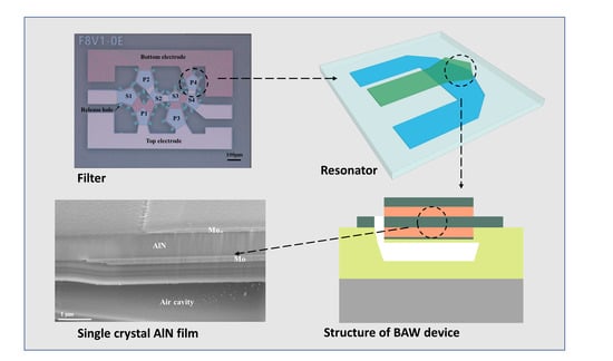
2. Fabrication of BAW Device
3. Results and Discussion
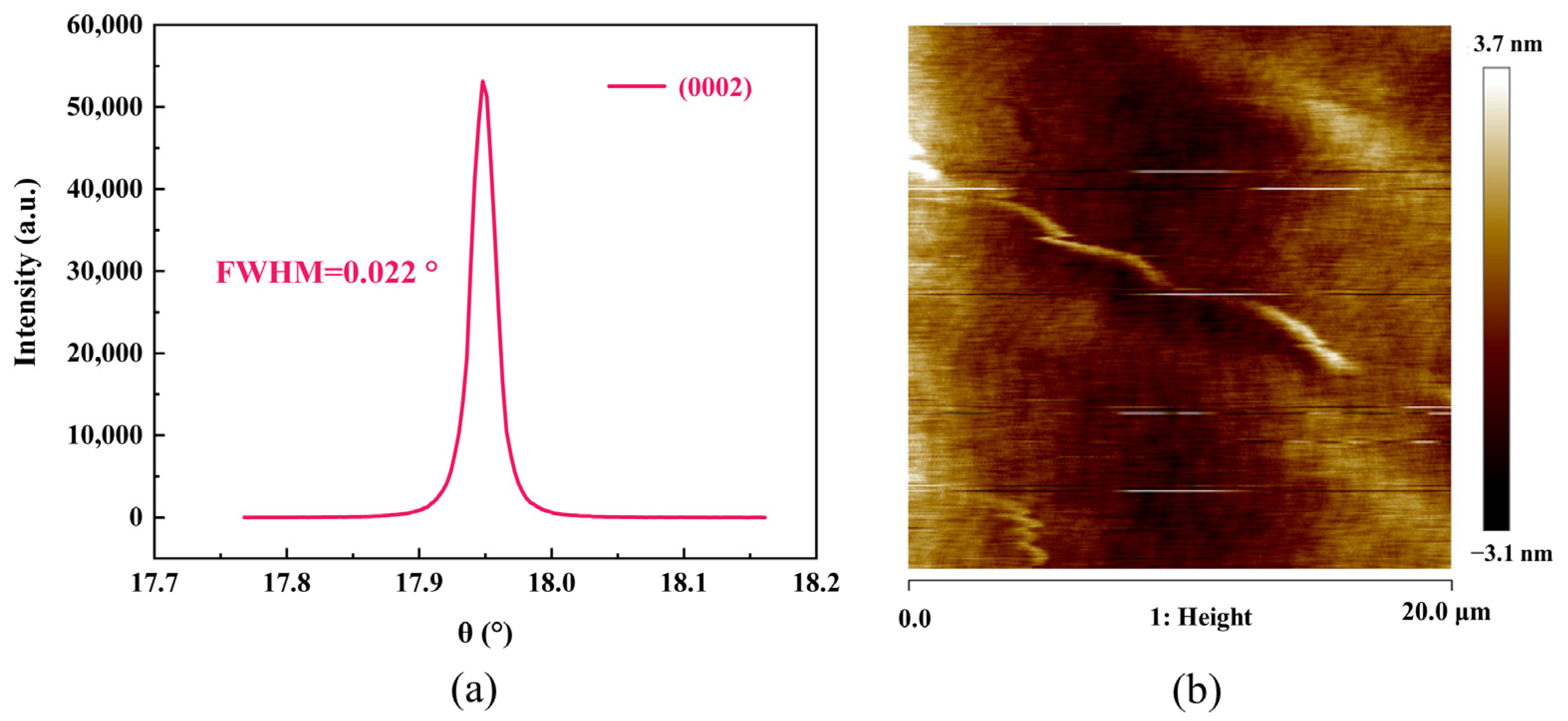
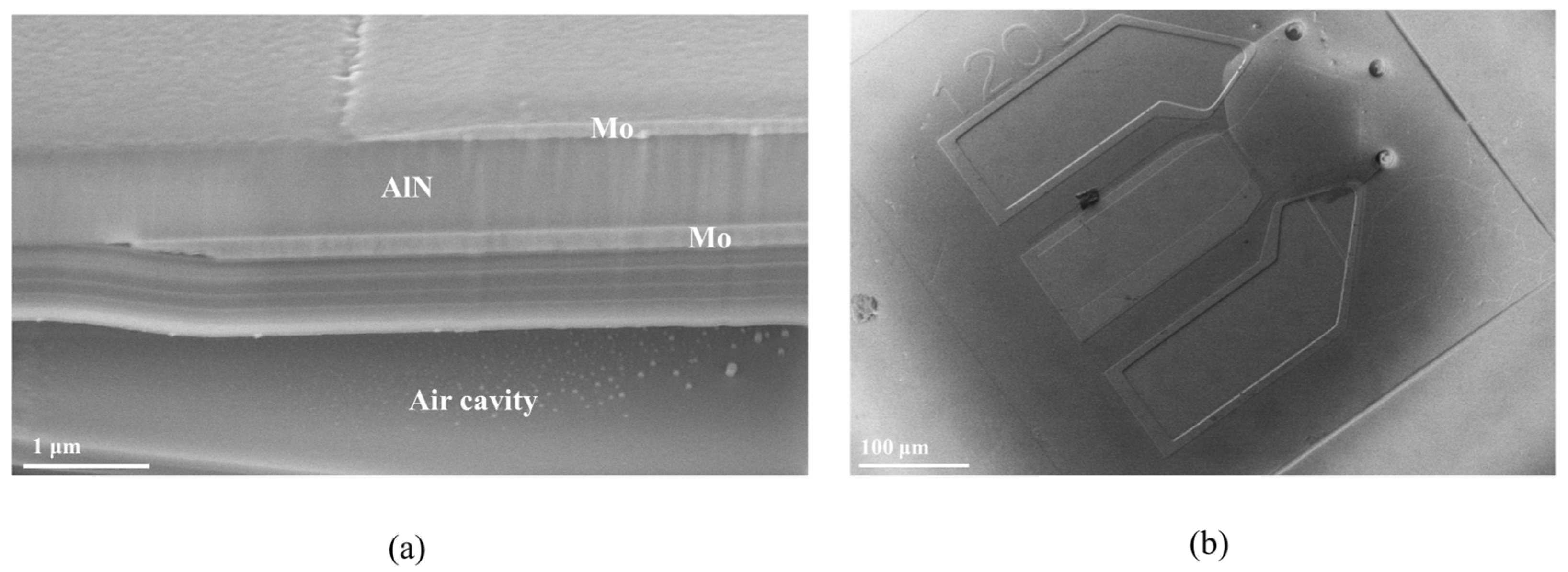
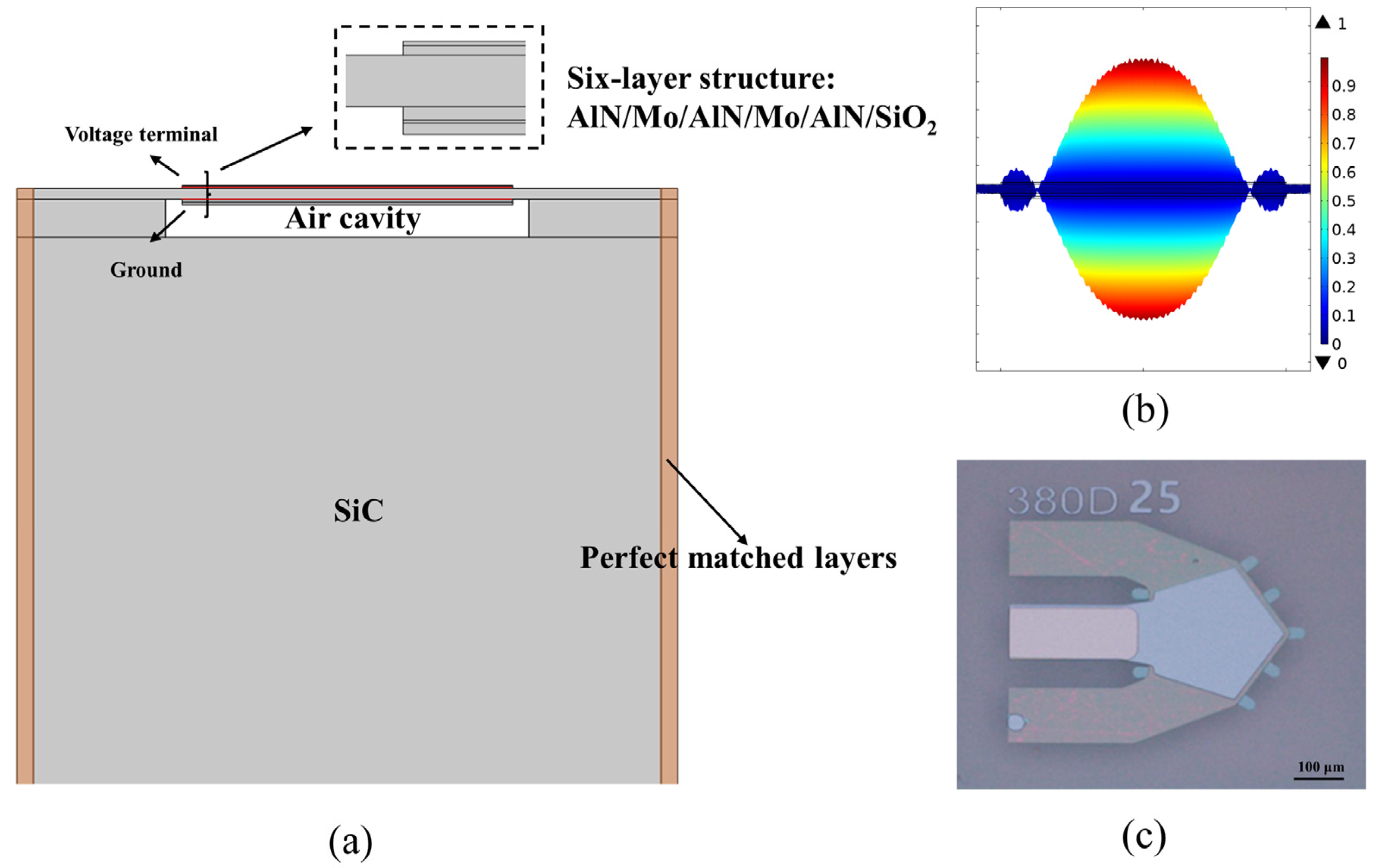
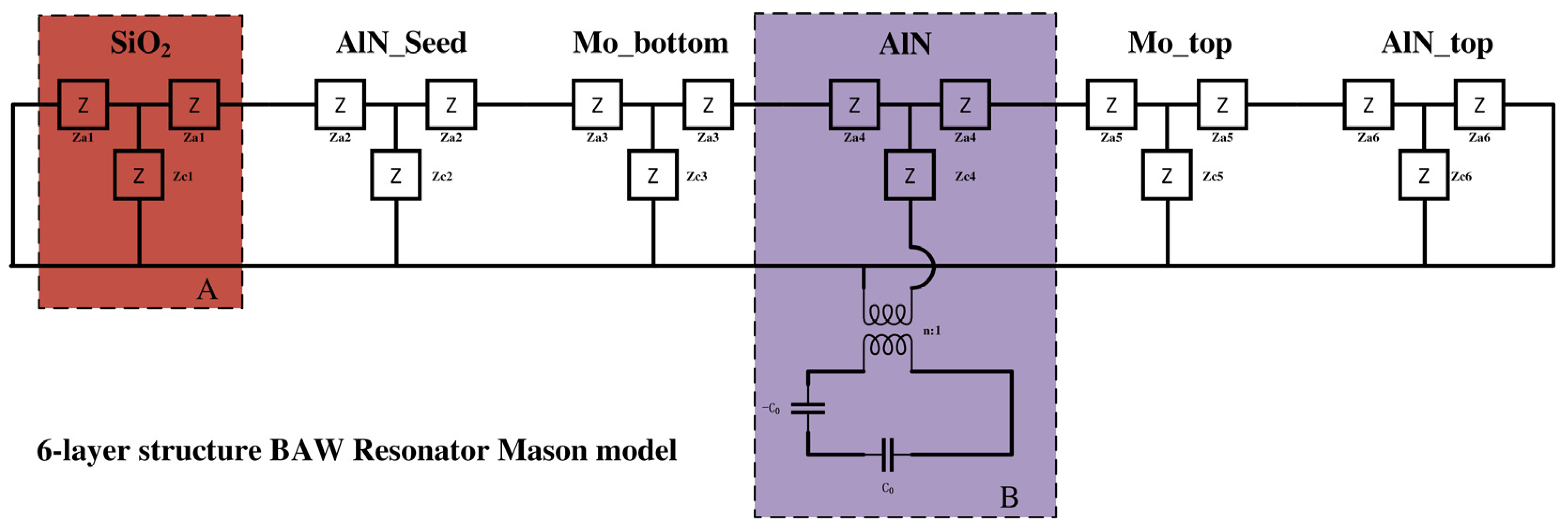
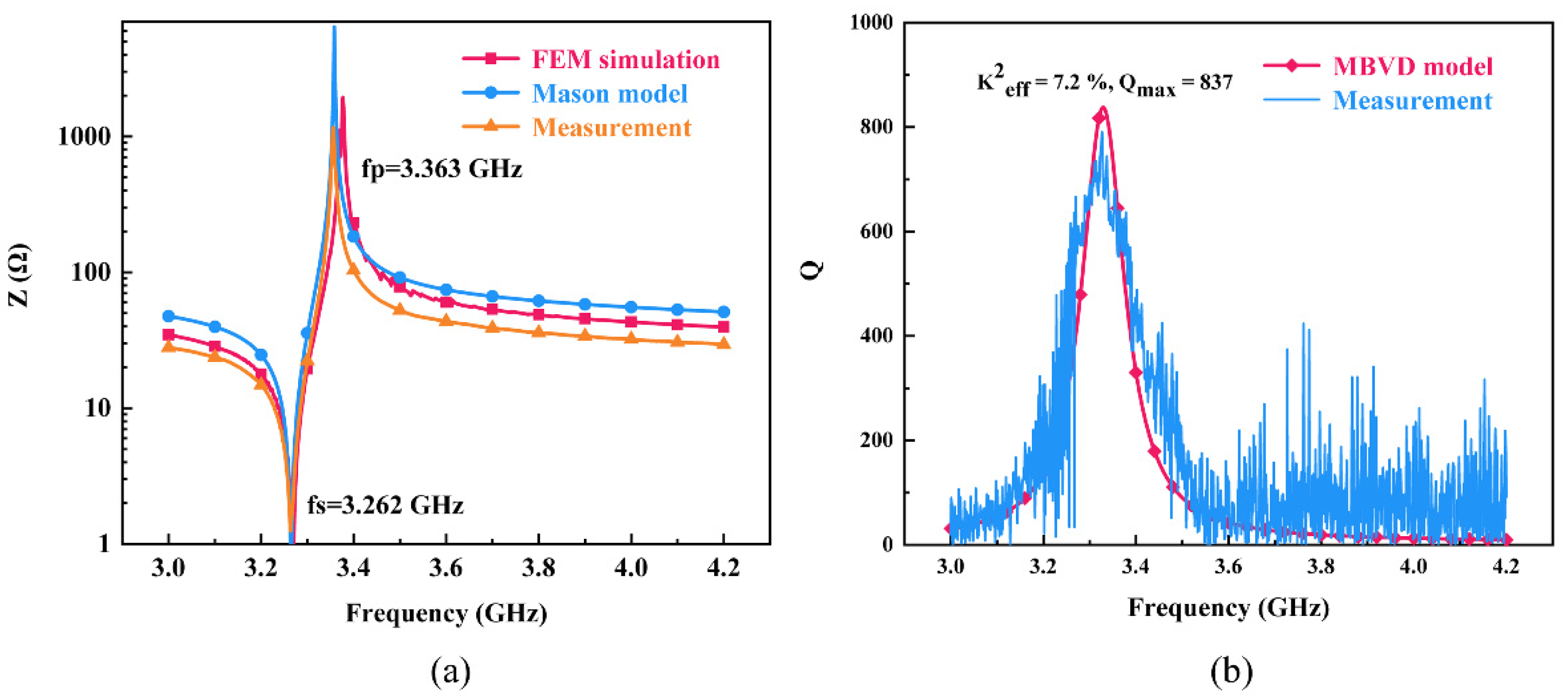
3.1. BAW Resonators
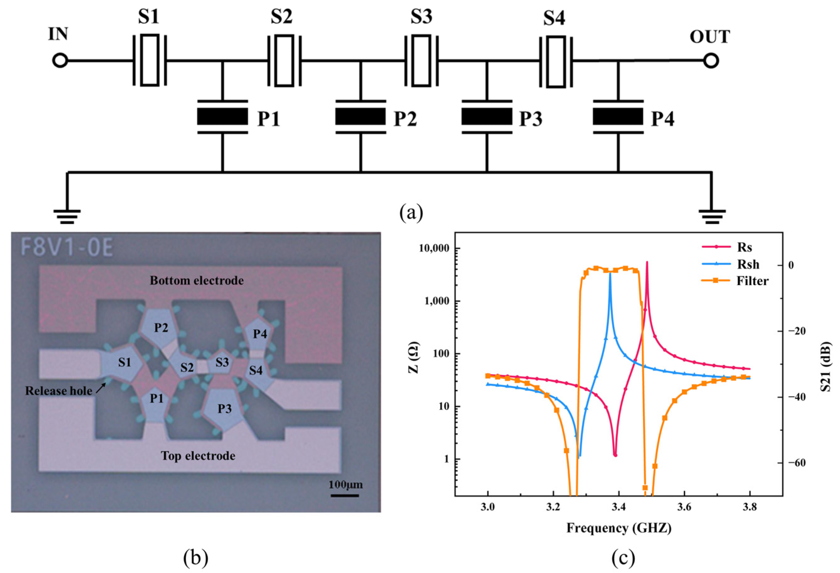
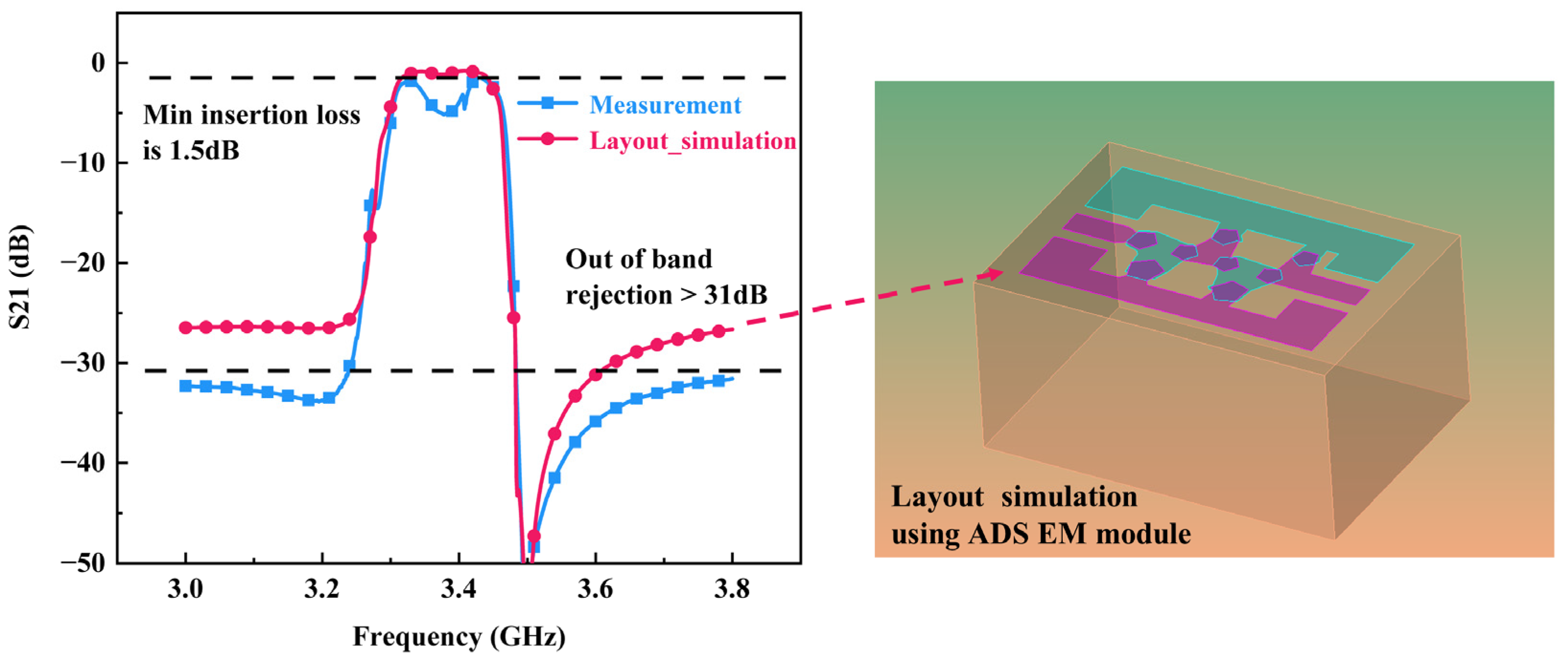
3.2. BAW Filters
4. Conclusions
Author Contributions
Funding
Institutional Review Board Statement
Informed Consent Statement
Data Availability Statement
Conflicts of Interest
References
- Gao, A.; Liu, K.; Liang, J.; Wu, T. AlN MEMS filters with extremely high bandwidth widening capability. Microsyst. Nanoeng. 2020, 6, 74. [Google Scholar] [CrossRef] [PubMed]
- Liu, Y.; Cai, Y.; Zhang, Y.; Tovstopyat, A.; Liu, S.; Sun, C. Materials, design, and characteristics of bulk acoustic wave resonator: A review. Micromachines 2020, 11, 630. [Google Scholar] [CrossRef] [PubMed]
- Hickman, A.L.; Chaudhuri, R.; Bader, S.J.; Nomoto, K.; Li, L.; Hwang, J.C.; Xing, H.G.; Jena, D. Next generation electronics on the ultrawide-bandgap aluminum nitride platform. Semicond. Sci. Technol. 2021, 36, 044001. [Google Scholar] [CrossRef]
- Shen, Y.; Zhang, R.; Vetury, R.; Shealy, J. 40.6 watt, high power 3.55 GHz single crystal XBAW RF filters for 5G infrastructure applications. In Proceedings of the 2020 IEEE International Ultrasonics Symposium (IUS), Las Vegas, NV, USA, 7–11 September 2020; pp. 1–3. [Google Scholar]
- Khosa, R.Y.; Chen, J.; Pálsson, K.; Karhu, R.; Hassan, J.; Rorsman, N.; Sveinbjörnsson, E.Ö. Electrical Characterization of MOCVD Grown Single Crystalline AlN Thin Films on 4H-SiC. In Proceedings of the 12th European Conference on Silicon Carbide and Related Materials, Birmingham, UK, 2–6 September 2018; Volume 963, pp. 460–464. [Google Scholar]
- Hodge, M.D.; Vetury, R.; Gibb, S.R.; Winters, M.; Patel, P.; McLain, M.A.; Shen, Y.; Kim, D.H.; Jech, J.; Fallon, K. High rejection UNII 5.2 GHz wideband bulk acoustic wave filters using undoped single crystal AlN-on-SiC resonators. In Proceedings of the 2017 IEEE International Electron Devices Meeting (IEDM), San Francisco, CA, USA, 2–6 December 2017; pp. 25–26. [Google Scholar]
- Shealy, J.B.; Vetury, R.; Gibb, S.R.; Hodge, M.D.; Patel, P.; McLain, M.A.; Feldman, A.Y.; Boomgarden, M.D.; Lewis, M.P.; Hosse, B. Low loss, 3.7 GHz wideband BAW filters, using high power single crystal AlN-on-SiC resonators. In Proceedings of the 2017 IEEE MTT-S International Microwave Symposium (IMS), Honolulu, HI, USA, 4–9 June 2017; pp. 1476–1479. [Google Scholar]
- Campanella, H.; Qian, Y.; Romero, C.O.; Wong, J.S.; Giner, J.; Kumar, R. Monolithic multiband MEMS RF front-end module for 5G mobile. J. Microelectromech. Syst. 2020, 30, 72–80. [Google Scholar] [CrossRef]
- Khine, L.; Wong, L.Y.; Soon, J.B.; Tsai, M.L.J. FBAR resonators with sufficient high Q for RF filter implementation. In Advanced Materials Research; Trans Tech Publications Ltd.: Bäch, Switzerland, 2011; pp. 70–73. [Google Scholar]
- Mason, W.P. Electromechanical Transducers and Wave Filters; Van Nostrand: New York, NY, USA, 1942. [Google Scholar]
- Shealy, J.B.; Shealy, J.B.; Patel, P.; Hodge, M.D.; Vetury, R.; Shealy, J.R. Single crystal aluminum nitride film bulk acoustic resonators. In Proceedings of the 2016 IEEE Radio and Wireless Symposium (RWS), Austin, TX, USA, 24–27 January 2016; pp. 16–19. [Google Scholar]
- Ruby, R.; Parker, R.; Feld, D. Method of extracting unloaded Q applied across different resonator technologies. In Proceedings of the 2008 IEEE Ultrasonics Symposium, Beijing, China, 2–5 November 2008; pp. 1815–1818. [Google Scholar]
- Feld, D.A.; Parker, R.; Ruby, R.; Bradley, P.; Dong, S. After 60 years: A new formula for computing quality factor is warranted. In Proceedings of the 2008 IEEE Ultrasonics Symposium, Beijing, China, 2–5 November 2008; pp. 431–436. [Google Scholar]
- Dubois, M.-A.; Billard, C.; Muller, C.; Parat, G.; Vincent, P. Integration of high-Q BAW resonators and filters above IC. In Proceedings of the ISSCC, 2005 IEEE International Digest of Technical Papers, Solid-State Circuits Conference, San Francisco, CA, USA, 6–10 February 2005; pp. 392–606. [Google Scholar]
- Shealy, J.B.; Hodge, M.D.; Patel, P.; Vetury, R.; Feldman, A.Y.; Gibb, S.R.; Boomgarden, M.D.; Lewis, M.P.; Shealy, J.B.; Shealy, J.R. Single crystal AlGaN bulk acoustic wave resonators on silicon substrates with high electromechanical coupling. In Proceedings of the 2016 IEEE Radio Frequency Integrated Circuits Symposium (RFIC), San Francisco, CA, USA, 22–24 May 2016; pp. 103–106. [Google Scholar]
- Vetury, R.; Kim, D.; Fallon, K.; Kwon, J.; Winters, M.; Gibb, S.; Patel, P.; Hodge, M.; Grundman, E.; McLain, M. Low Loss, Wideband 5.2 GHz BAW RF Filters Using Single Crystal AlN Resonators on Silicon Substrates. Gan 2018, 6, 1130. [Google Scholar]


| Shunt Resonator | Series Resonator | |||
|---|---|---|---|---|
| fs/GHz | fp/GHz | fs/GHz | fp/GHz | |
| Simulated | 3.279 | 3.374 | 3.388 | 3.486 |
| Measured | 3.265 | 3.356 | 3.406 | 3.498 |
| Ref. | Freq. | Piezoelectric Layer | (Resonator) | Q (Resonator) | Min. Insertion Loss (Filter) | Size (Filter) |
|---|---|---|---|---|---|---|
| [7] | 3.8 GHz | AlN | 5.87% | 1572 | 2.01 dB | 1.25 × 0.9 mm2 |
| [14] | 2.1 GHz | AlN | 6.50% | 900 | 2.15 dB | 1.2 × 0.85 mm2 |
| [15] | 2.3 GHz | AlGaN | 4.44% | 1277 | — | — |
| [16] | 5.2 GHz | AlN | 6.07% | 1497 | 2.00 dB | ~1 × 0.7 mm2 |
| this work | 3.4 GHz | AlN | 7.20% | 837 | 1.60 dB | 0.6 × 0.35 mm2 |
Publisher’s Note: MDPI stays neutral with regard to jurisdictional claims in published maps and institutional affiliations. |
© 2022 by the authors. Licensee MDPI, Basel, Switzerland. This article is an open access article distributed under the terms and conditions of the Creative Commons Attribution (CC BY) license (https://creativecommons.org/licenses/by/4.0/).
Share and Cite
Ding, R.; Xuan, W.; Dong, S.; Zhang, B.; Gao, F.; Liu, G.; Zhang, Z.; Jin, H.; Luo, J. The 3.4 GHz BAW RF Filter Based on Single Crystal AlN Resonator for 5G Application. Nanomaterials 2022, 12, 3082. https://doi.org/10.3390/nano12173082
Ding R, Xuan W, Dong S, Zhang B, Gao F, Liu G, Zhang Z, Jin H, Luo J. The 3.4 GHz BAW RF Filter Based on Single Crystal AlN Resonator for 5G Application. Nanomaterials. 2022; 12(17):3082. https://doi.org/10.3390/nano12173082
Chicago/Turabian StyleDing, Rui, Weipeng Xuan, Shurong Dong, Biao Zhang, Feng Gao, Gang Liu, Zichao Zhang, Hao Jin, and Jikui Luo. 2022. "The 3.4 GHz BAW RF Filter Based on Single Crystal AlN Resonator for 5G Application" Nanomaterials 12, no. 17: 3082. https://doi.org/10.3390/nano12173082
APA StyleDing, R., Xuan, W., Dong, S., Zhang, B., Gao, F., Liu, G., Zhang, Z., Jin, H., & Luo, J. (2022). The 3.4 GHz BAW RF Filter Based on Single Crystal AlN Resonator for 5G Application. Nanomaterials, 12(17), 3082. https://doi.org/10.3390/nano12173082