1. Introduction
Solar energy is considered a basis to obtain clean and abundant energy; therefore it has become essential to take advantage of solar radiation as an energy source in the field of photovoltaics [
1]. Recently, organic and inorganic perovskites, especially those based on methylammonium halides, have become attractive and promising research materials. Perovskite solar cells (PSC) showing power conversion efficiencies higher than 23% have been reported [
2]. Perovskite materials also have remarkable optical and electronic properties, as they allow light to be absorbed in a wide wavelength for a long time, charge carriers to have a long diffusion length, and excitons to have small binding energy, which produces electrons and holes [
3,
4,
5]. Furthermore, for perovskite thin film fabrication, a variety of techniques have been used, including one-step and two steps deposition [
6], evaporation [
7], and thermal deposition [
8]. One-step deposition carried out via spin coating demonstrated an excellent capability to fabricate PSCs. Moreover, the PSCs showed homogeneous and compact thin films when fabricated using the spin coating technique. It has been shown that the morphology of perovskite thin films plays a vital role in device performance. Many methods and treatments have been introduced to optimize the product quality by improving the surface homogeneity and crystallinity of the films. To achieve a good crystallization of thin films, several strategies are used, such as evaporation, cooling, heating, addition of an antisolvent—also in combination—so to slow the solubility in a saturated solution. The film surface’s supersaturation level and thermal annealing were investigated by adding different antisolvents. Several physicochemical properties affect this process, resulting in complex exchanges occurring simultaneously. Improving the performance of solar cells requires a thorough understanding of the mechanisms involved and the proper use of adequate antisolvent treatments [
9,
10].
A PSC with methylammonium lead iodide (MAPbI
3) as an absorber has the highest conversion efficiency, but lead (Pb) contained in the material may have dramatic health consequences; therefore, it is highly appropriate and necessary to explore the possibility of substituting tin (Sn) for lead in MAPbI
3 and improve the efficiency and stability of MASnI
3-based solar cells. Investigations should start by analyzing the growth of the absorber layer to achieve high crystallinity and optimal morphology, as these features are essential for improving the optical properties of the absorber. Recently, the use of tin halide perovskites as absorbers has been investigated. MASnI
3-based solar cells are considered good candidates for perovskite solar cells. It has been demonstrated that MASnI
3 PSC have a power conversion of 6.4% under one sun illumination with an open circuit voltage of 0.88 V. However, their performance varies widely because of an uncontrollable doping effect caused by the introduction of Sn
4+ through the oxidation of Sn
2+. Suppressing Sn
2+ oxidation is, therefore, an appropriate approach to improving and stabilizing the device performance; this can be achieved by adding SnF
2 or excess SnI
2, Furthermore, the fabrication process greatly affects the morphology of the perovskite layer. Since tin perovskite crystallizes rapidly and is very soluble, fabrication methods are limited for tin perovskite films [
11,
12,
13,
14].
In this work, MASnI3 films were treated with different antisolvents to see how they affected the supersaturation of the solvent. We report that complex interactions between the solvent and the antisolvent are related to the film’s physicochemical properties; therefore, choosing the antisolvent type is critical to improve the perovskite film’s morphology and, in turn, boost the PSC performance. The antisolvent effects manifested in the variation of morphology, structure, and composition of the thin films. Toluene (TOL), chlorobenzene (CBZ), and diethyl ether (ET) were the antisolvents used in this investigation. The obtained MASnI3 samples were further analyzed by other characterization techniques such as XRD, SEM, and optical and PL analyses. Additionally, we produced the device FTO/TiO2/MASnI3/Spiro-OMeTAD/Au, which demonstrated an amazing PCE.
2. Experimental Procedure
2.1. Materials
Tin (II) iodide (SnI2) was purchased from Alfa Aesar, Haverhill, MA, USA, methylammonium iodide (MAI) with the formula CH6NI was purchased from Tokyo Chemical Industry, Oxford, UK. N,N-dimethylformamide (DMF) and dimethyl sulfoxide (DMSO) were purchased from Sigma Aldrich, Madrid, Spain, and used for manufacturing the optoelectronic devices. The volume of DMF used was 1ml, while that of DMOS was 95 μL. Diethyl ether anhydrous (ET), chlorobenzene (CBZ), and toluene (Tol) were used as antisolvents, were all purchased from Sigma Aldrich Madrid Spain, and were used as received. Fluorine tin oxide-coated glass (FTO) was used as a substrate with Sheet Resistance of 6–9 Ω/square and Roughness of 34.8 nm.
2.2. Film Preparation
The FTO substrates were washed for 15 min in soap, ethanol, acetone, and isopropanol. Compressed air was used to dry the FTO glass. Afterward, the FTO substrates were put in a UV–ozone cleaner for 15 min to eliminate contaminations and wetness on the surface. The FTO substrates were then placed under an inert atmosphere of argon, together with MASnI3 samples until characterization could be undertaken. For the elaboration of the films, a 1 M solution of MASnI3 was prepared by dissolving equimolar ratios of MAI and SnI2 in 1 mL of DMF and 95 μL DMSO at 60 °C for 2 h. When the solution was ready, 50 µL of MASnI3 solution was statically spin-coated at 2000 rpm for 20 s, and 100 µL of one of the antisolvents was applied after a certain time from the initiation of the spin program, referred to as the optimized dripping time of 12 s. Then, MASnI3 samples were annealed for 5 min at 50 °C, and their surface became black. This initial color change was due to the growth of the perovskite structure; MA requires relatively little energy to begin intercalating between SnI2. To avoid thermal shocks, the samples were heated slowly to 100 °C and held there for 5 min, removing any remaining solvent. The samples became dark during this stage of annealing, indicating that the perovskite phase had completely formed. Afterwards, the prepared solution of MASnI3 was spin-coated onto the FTO substrate at 2000 rpm for 20 s. Different antisolvents were dripped onto the MASnI3 thin films, and subsequently, the as-prepared MASnI3 samples were annealed in a vacuum for 20 min at 250 °C. The deposition and annealing processes were carried out in a glove box where all samples were stored until characterization; they were termed fresh samples.
The crystal structure analysis of perovskite thin films was performed using an XRD RIGAKU Ultima IV diffractometer with Cu kα radiation (λ = 1.5418 Å). Surface morphology was investigated through SEM at different magnifications within the Zeiss Auriga Compact, with an applied voltage of 1.5 kV. The film’s topography was characterized using a cross section. The absorption was measured in a UV–visible wavelength range from 300 to 850 nm with an Ocean Optics HR4000 spectrophotometer, and PL was performed using a He–Cd laser driven by a semiconductor laser with a wavelength of λ = 405 nm.
2.3. Device Preparation: Gold/Spiro OMeTAD/MASnI3/Compact–TiO2/FTO/Glass
The MASnI3 devices were made onto FTO-coated substrates. Here are the steps involved in the entire process:
- (1)
The substrates were cut obtaining samples with a size of 2.5 × 2.5 cm2.
- (2)
Zinc powder was sprinkled over the area of the FTO substrate that we wished to etch in a customized holder. This step involved partially etching the FTO substrates where the zinc powder was sprayed with concentrated HCl (2 M).
- (3)
An ultrasound bath was used to wash the etched substrates with 2% Hellmanex solution for 15 min; then, the substrates were dipped in deionized water. A UV–ozone cleaner was used to treat the etched substrates for 15 min after washing with ethanol, acetone, and isopropanol using the same method and air-drying.
- (4)
Spray pyrolysis was used to deposit the first TiO2 electron blocking layer. TiO2 was deposited using titanium diisopropoxide bis (acetylacetonate) diluted in ethanol with oxygen as the carrier gas, by spin coating and heating at 500 °C for 30 min.
- (5)
Then, the as-prepared solution of MASnI3 was spin-coated at 2000 rpm for 20 s and annealed at 100 °C for 5 min on FTO/TiO2.
- (6)
Afterwards, 50 μL of the Spiro-OMetad solution was deposited by spin coating at 4000 rpm for 30 s on top of MASnI3/TIO2/FTO. The solution was prepared with 28.8 μL of 4-tert-butylpyridine and 17.5 μL of a stock solution of 520 mg mL−1 of lithium bis-(tri-fluoromethylsulfonyl) imide in acetonitrile and by dissolving 72.3 mg of (2,2′ 7,7′-tetrakis(N,N’-di-p-methoxyphenylamine)-9,9′-spirobifluorene) in 1 mL of chlorobenzene.
- (7)
At the end of the elaboration process of the solar device, a thin layer of gold contact was thermally evaporated on the top of the device.
- (8)
In order to determine the J–V characteristic curve of the as-deposited photovoltaic devices, we used the Abet Solar simulator with a 1.5 AM filter. A mask was used to define a 0.1 cm2 active area for the devices.
2.4. Experiment Structure
The samples were prepared, and with Tol, ET, and CBZ were used as antisolvents. The dripping time for all samples was 10 s; 100 µL of each of the different antisolvents was applied. The samples were characterized by XRD, UV–vis spectroscopy, PL, and FESEM. At the end of the experiment, XRD and SEM images were used to determine the stability. During the process of antisolvent selection, all samples were kept in the laboratory for the degradation study at 23 °C and a relative humidity of 60% for 4 weeks. Daily temperature measurements revealed only small fluctuations of 2 °C. Due to heavy precipitation outside, the relative humidity decreased to 53% for a few days during the experiment. All samples were exposed to the same conditions, allowing for a fair comparison between them. To manufacture the Spiro-OMeTAD/MASnI3/TiO2/FTO device, the TiO2 film was prepared outside the glovebox after the perovskite layer and spiro-OMeTAD were deposited inside the glovebox; then, the gold layer was thermally evaporated on the top of the device.
3. Results and Discussion
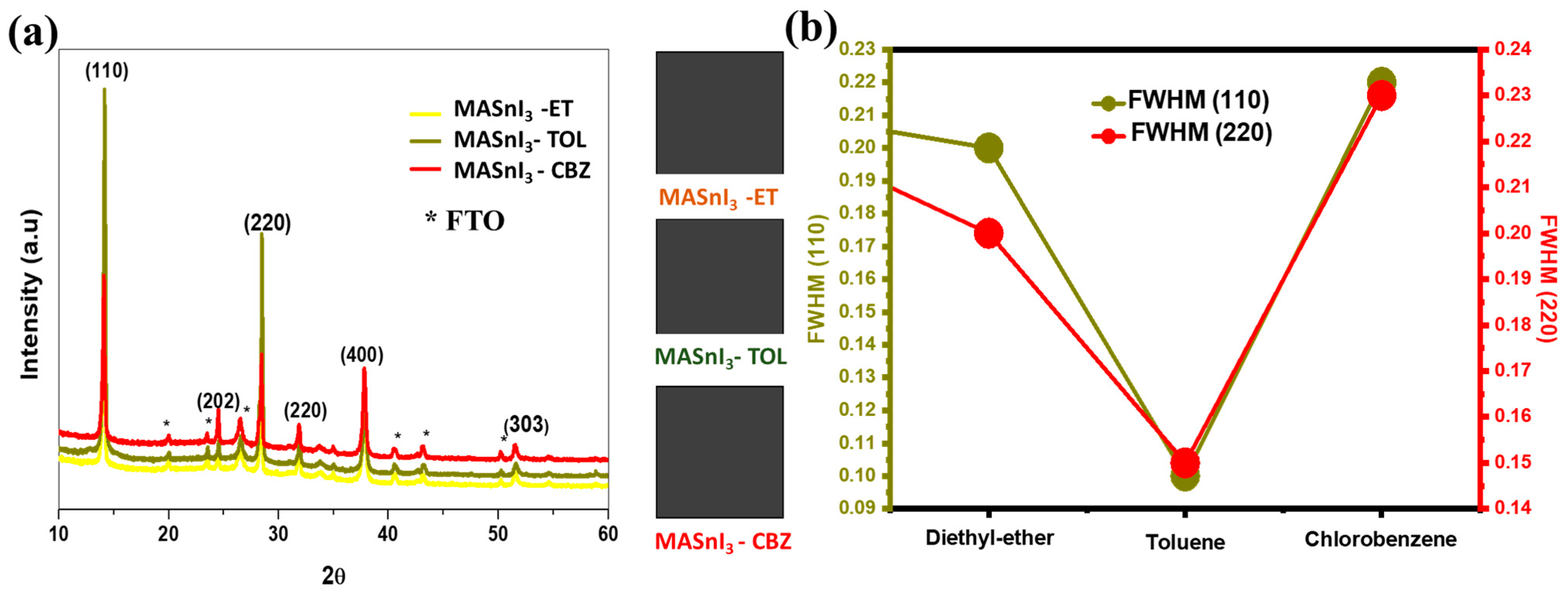
The influence of the antisolvent on the films’ phase structure and microstructure was studied by XRD.
Figure 1 shows the X-ray diffraction patterns of the MASnI
3 films treated with different antisolvents. The diffraction peaks that appeared at 14°, 28°, 31°, 38°, and 31° correspond to the (110), (220), (222), (224), and (314) peaks, respectively. These results are in good agreement with previous findings [
15,
16]; the FTO peaks are identified by the star symbol, The XRD results of the prepared MASnI
3 films indicated good crystallinity. The intensity of the characteristic (110) peak increased enormously when toluene was used as an antisolvent compared to chlorobenzene and diethyl ether. The intensity decrement can be attributed to the excessive solubility of methylammonium iodide (MAI).
Lattice Parameters
The lattice parameters were calculated using Equations (l) and (2) with two different theta diffraction angles:
where
a,
b,
c are the lattice parameters,
h,
k,
l are Miller indices,
dhkl is the interplanar distance, and
k is the wavelength (0.154 nm).
The obtained lattice parameters of the main (110) peak were a = b = 8 Å, c = 11.9 Å, corresponding to the tetragonal structure.
Lattice Strain and Dislocation Density.
The lattice strain (ԑ) indicates a thin film’s crystal deformation calculated from Equation (3). The results obtained between 340 nm and 400 nm are summarized in
Table 1.
where
β is the FWHM value, k is the dielectric constant, with the value k = 0.9,
λ is the X-ray wavelength (
λ is 0.1540 nm),
θ is the Bragg diffraction angle, and
D is the crystallite size (nm). Equation (4) below shows the estimated grain size dislocation density:
Table 1 shows that the three samples had different grain sizes, from 300 nm to 400 nm, when MASnI
3 was treated with different antisolvents. The larger grain size of 400 nm was obtained with toluene. The lower effective lattice around 0.37 is explained by less deficiencies and distortions of the grains.
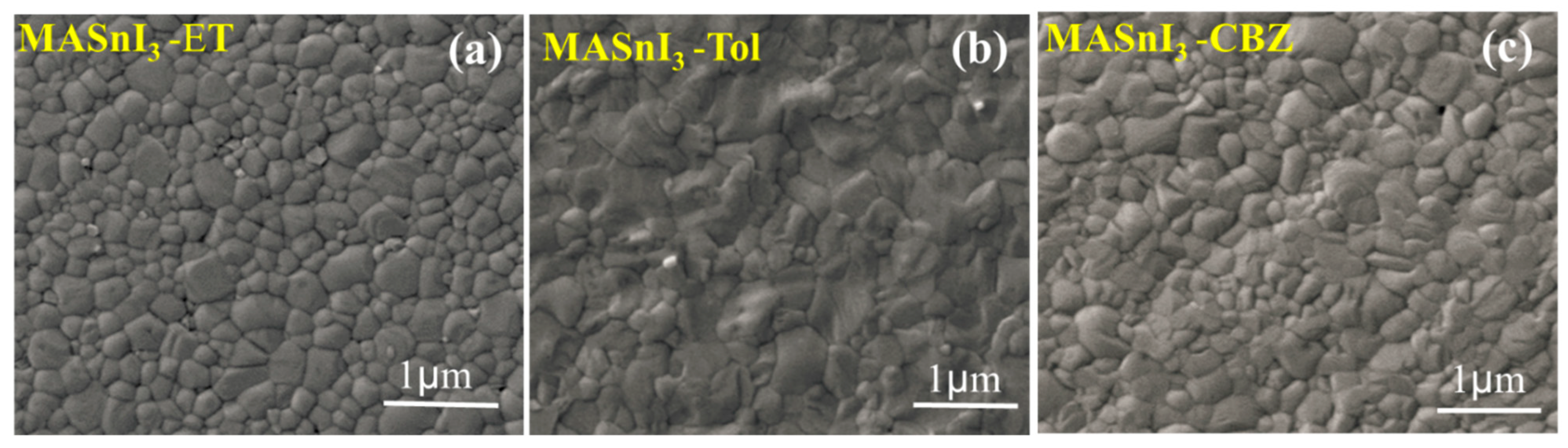
Figure 2 shows SEM images of MASnI
3 treated with different antisolvents. The antisolvent quenching techniques presented here improved the crystalline quality of MASnI
3 thin films and extended their lifetime. The antisolvent, in our case a perovskite solution, could not dissolve its components. Local regions of supersaturation are created when an antisolvent is applied, accelerating heterogeneous nucleation. High-quality films are obtained by optimizing the nucleation rate and the crystal growth rate. Generally, the antisolvent concentrations are kept high, on the basis of the solubility curve, and under the metastable limit on the seeding zone. These concentrations allow the growth of existing nuclei, or “seeds”, without creating new ones. The surface morphology of MASnI
3 was examined with SEM. It was found that with diethyl ether, crystals poorly formed. Even chlorobenzene did not change significantly the morphology of the film. However, toluene significantly altered the films’ morphology, leading to the largest crystal size. These observations indicated that the morphology of MASnI
3 changed in relation to the type of antisolvent [
17,
18]. The addition of antisolvent also produced fine needles that agglomerated easily. This proved that supersaturation plays a vital role in a crystallization system and influences the crystals’ size, shape, and degree of accumulation [
19,
20]. The remaining solvent is removed under 250 °C during the annealing treatment. The conversion of precursors in the perovskite phase was almost perfect in all samples, but the goal was to affect the surface.
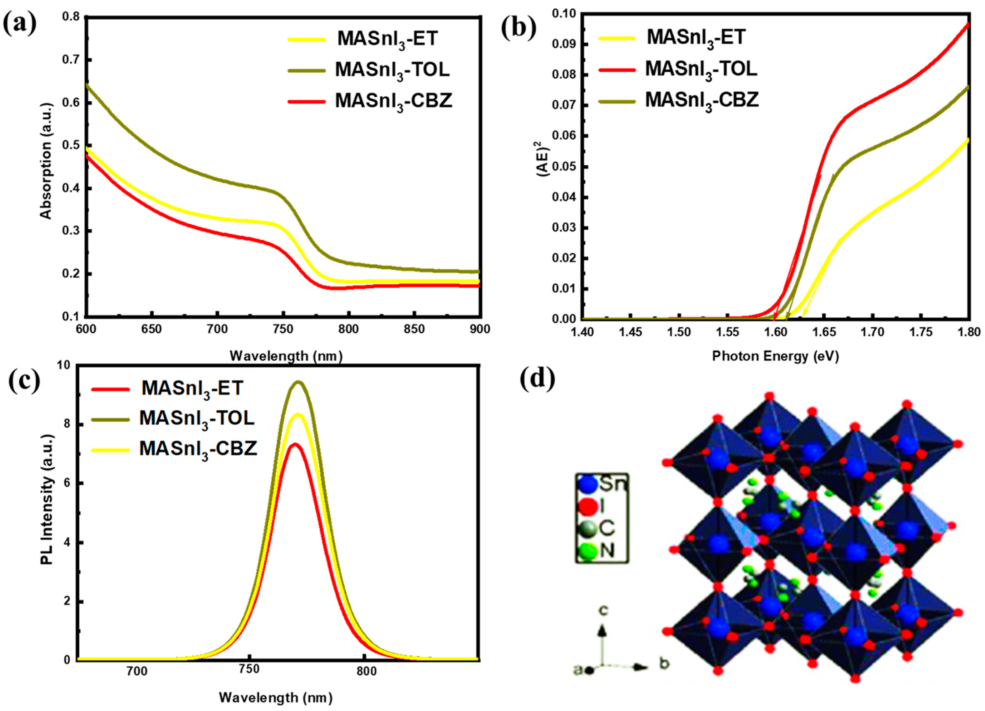
All samples displayed a time-dependent PL spectrum under illumination and a high energy peak, as shown in
Figure 3. Furthermore, storing a sample in dark conditions would “reset” the spectrum. Other authors made similar observations, and the “Hoke Effect” was also observed [
21].
Figure 3 shows the characteristic PL peak of the three MASnI
3 samples treated with different antisolvents, i.e., toluene, chlorobenzene, and diethyl ether, applied in the wavelength range from 750 to 800 nm [
22]. The PL peak of the MASnI
3 sample treated with toluene showed a higher intensity than that of the MASnI
3 sample treated with diethyl ether or chlorobenzene. The MASnI
3 sample treated with toluene also showed an optimal bandgap around 1.58 eV, calculated from the PL spectrum; the band gap calculated from the UV–visible spectrum was 1.6 eV, and the Stokes shift of MASnI
3 treated with toluene showed a low value (
Table 2). This can be related to phase transitions commonly found for halide perovskite [
23,
24,
25].
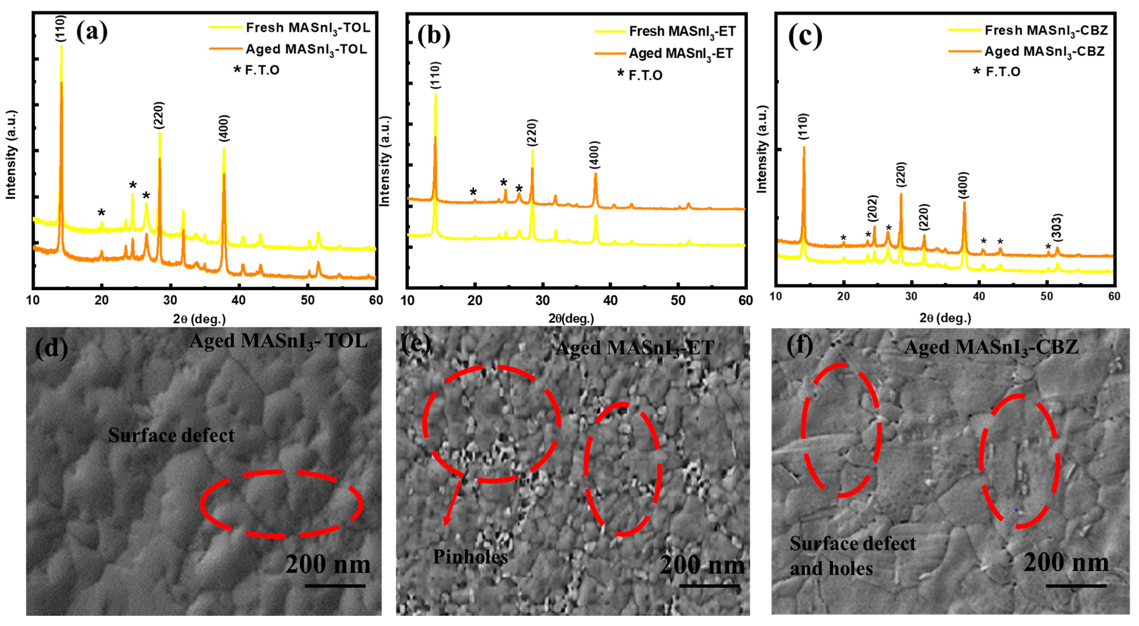
4. Degradation Study
Oxygen and humidity significantly impact the stability of perovskite solar cells. Once the film is exposed to extreme environmental conditions, its degradation is due to the reduction to SnI
2, MAI, and HI [
26,
27,
28,
29].
The stability of MASnI3 films was examined after four weeks from the treatment with the three antisolvents. To investigate the degree of degradation of the MASnI3 films, both fresh and four-week-old MASnI3 samples were analyzed by XRD and SEM; the MASnI3 aged samples were kept under 60% humidity in a dark environment.
The XRD patterns for the four-week-old MASnI
3 films treated with chlorobenzene and toluene antisolvents showed a slightly reduced intensity of the characteristic peaks (110) and (220) when compared to those of MASnI
3 films treated with diethyl ether, which displayed a dramatic increase in the intensity of these peaks (
Figure 4a–c). In this regard, chlorobenzene and toluene as antisolvents enhanced the stability of the MASnI
3 films more than diethyl ether. The SEM images also supported this finding (
Figure 4d–f). The surface morphology changes are observed in the SEM images of aged MASnI
3 films with new grain boundaries and new defects. Therefore, the degradation process differs between the antisolvent-treated films.
5. Device Performance
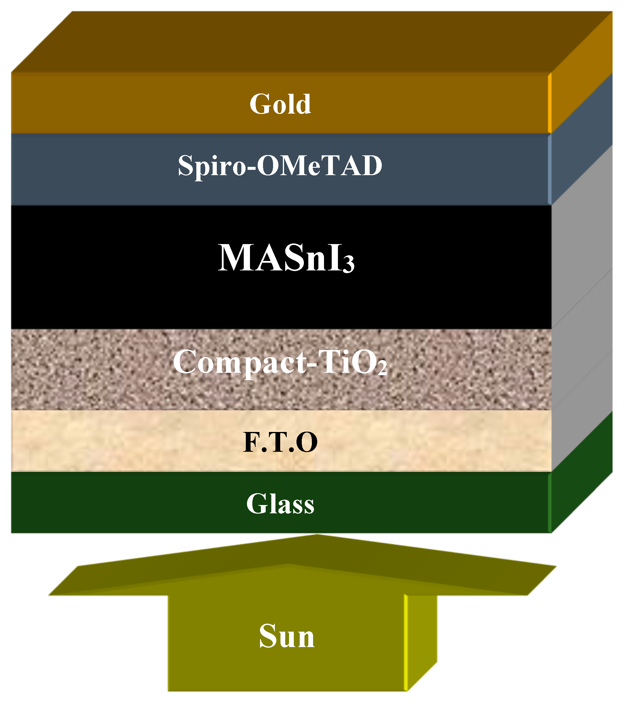
We observed that the film thickness varied when different antisolvents were used, and similarly, the bandgap varied when MASnI3 was used. PSCs are more sensitive to variation in thickness related to the bandgap of their absorbing layers. As part of the simulations, we modeled the proposed solar cell in order to further analyze the impact of different antisolvents on its performance. In “Gold/Spiro-OMeTAD/MASnI3/Compact-TiO2/FTO/Glass”, MASnI3 was used as an absorber, Spiro-OmeTAD as a hole transport layer (HTL), Compact-TiO2 (C-TiO2) as an electron transfer layer (ETL), without taking into consideration mesoporous-TiO2 in the simulation model, and FTO was used as a substrate.
Supplementary Table S1 and
Table 3 provide a list of the simulation parameters used in SCAPS-1D software.
Table 1 shows our experimental calculations, which we used in
Table 2. The work function for back and front contact was used as default in SCAPS-1D. The proposed solar cell structure used in SCAPS-1D was arranged as shown in
Figure 5. The layers of the cell are depicted in
Figure 5.
The SCAPS-1D software version 3.3.10 was run under 1000 W/m
2 illumination and at ambient temperature (300 K). The series resistance and shunt resistance were kept negligible and infinite, respectively, which are ideal values that experimentally do not exist up to these limits. The bandgap and thickness of MASnI
3 are shown in
Table 3.
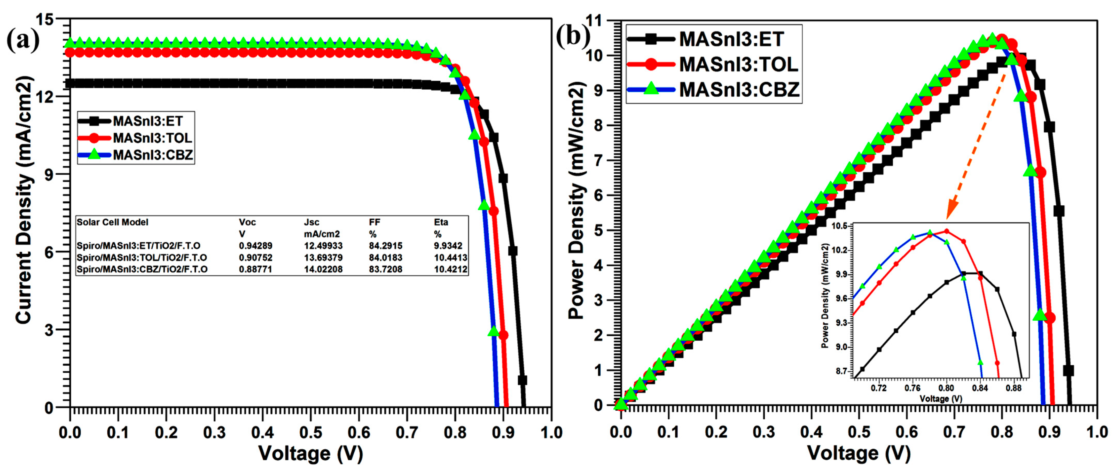
Figure 6a,b illustrate the J–V and P–V curves for MASnI
3, respectively, and demonstrate how the different antisolvents affected the results. Toluene had a positive impact on the device; the P–V angles delivered the highest power when using toluene as an antisolvent.
Diethyl ether antisolvent-based MASnI
3 produced V
oc of 0.94 V, J
sc of 12.49 mA/cm
2, FF of 84.29%, and Eta of 9.93% during the simulation of solar cells. We notice that diethyl ether is less effective because, chlorobenzene V
oc, J
sc, FF, and Eta were registered as 0.88 V, 14.02 mA/cm
2, 83.72%, and 10.42%, respectively, which was good in comparison to when ET was used as antisolvent as shown in
Table 4.
In summary, Toluene is the most profitable antisolvent because it gave excellent results compared to the other two antisolvents. With Toluene treatment for MASnI3 films, we record Voc, Jsc, FF, and Eta as 0.90 V, 13.69 mA/cm2, 84.01%, and 10.44%, respectively.
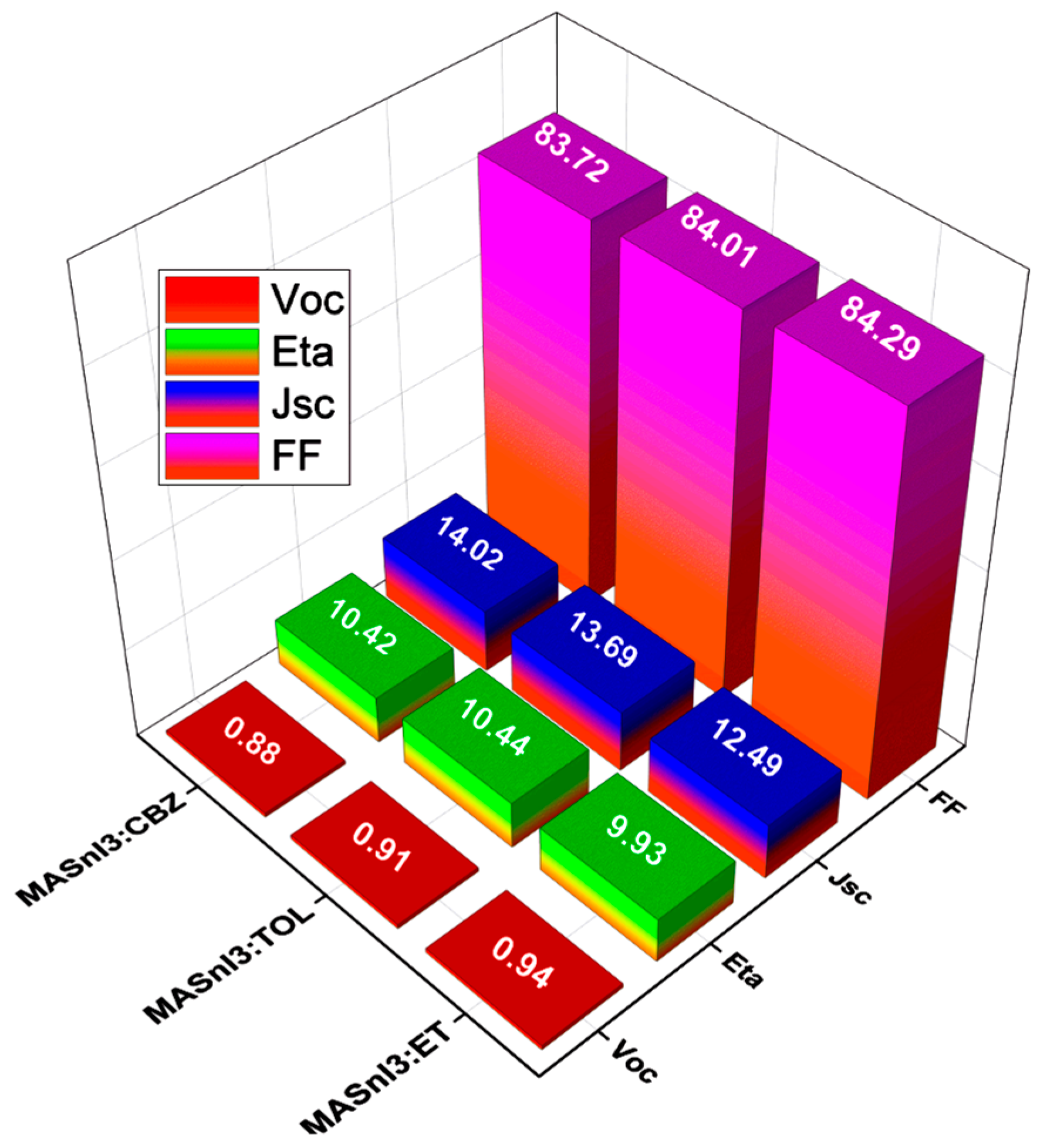
Here, in
Figure 7, we compare the characteristic parameters of MASnI
3 solar cells based on different antisolvents used in the solution. We can observe that toluene would be the optimal antisolvent for preparing the MASnI
3 absorber layer as it gives us the best results of the characteristic parameters for the solar device.
6. Manufacture of the Spiro-OMeTAD/MASnI3/C-TiO2/FTO Device
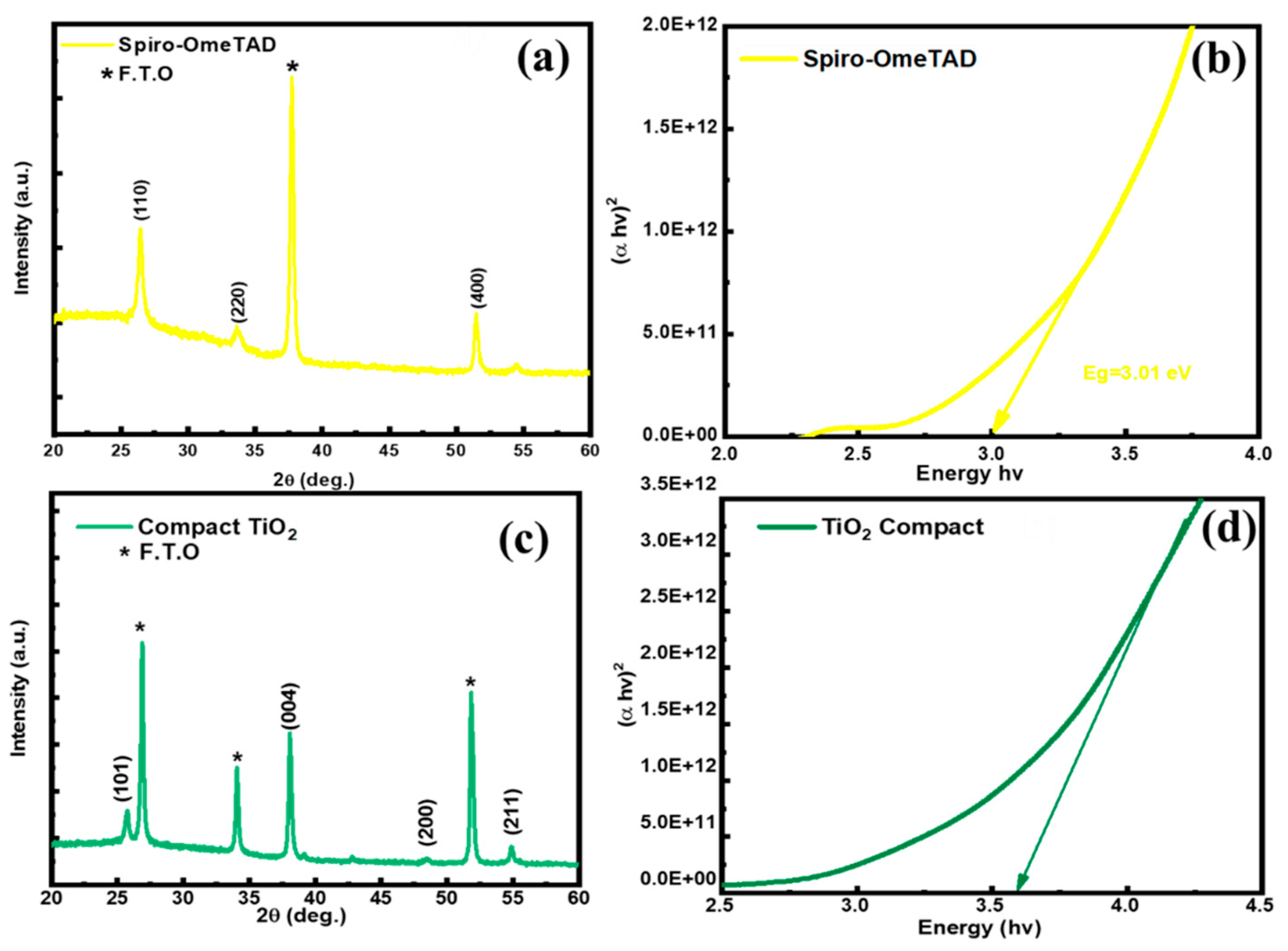
We report the XRD analysis for the Spiro-OMeTAD film with characteristic peaks at (110), (220), and (400) (
Figure 8a). These results are in agreement with previous studies [
30]. When calculating the experimental bandgap after absorbance characterization, we obtained 3.0 eV, which is the optimal bandgap, also previously reported [
31]. For compact TiO
2, the XRD spectrum showed characteristic peaks at (101), (004), (200,) and (211) (
Figure 8c). We found the same characteristic peaks when comparing these XRD spectrum with those in the literature [
32]. The absorption analysis for TiO
2 revealed an experimental bandgap of 3.6 eV (
Figure 8d).
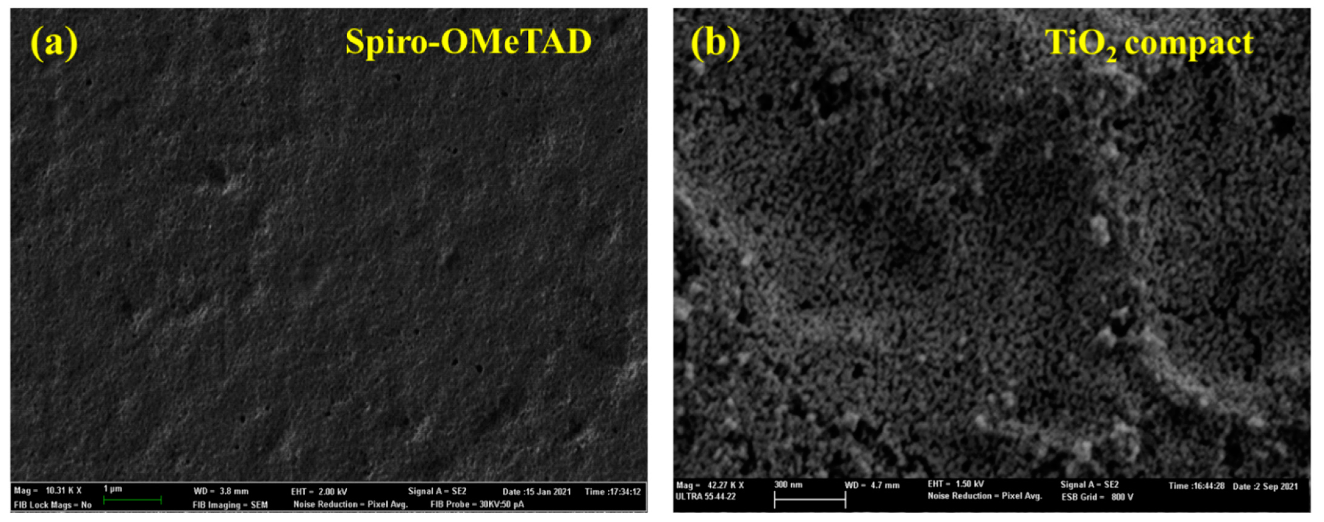
Figure 9 shows SEM images of both the Spiro-OMeTAD and the TiO
2 layers. The SEM image of the TiO
2 films showed a smooth and homogenous surface. The Spiro-OmeTAD film showed a regular surface with no holes.
The device Spiro-OMeTAD/MASnI3/C-TiO2/FTO was fabricated. The thickness of TiO2 was approximately 200 nm, that of the MASnI3 film was between 300 and 400 nm, and that of the Spiro-OMeTAD layer was around 100 nm. The gold layer had a thickness of around 50 nm.
The results of four planar devices named Sx (x = (1, 2, 3, 4)) containing four separated pixels are presented. Each showed high efficiency, resulting in 30 solar cells manufactured simultaneously under similar conditions. Pixel number S x_1 refers to the first pixel in cell Sx. The cells were concealed in a metal aperture with an area of 0.1cm2.
A solar simulator was used to measure the device efficiencies and curves within 24 h from the thermal evaporation of gold on the surface to obtain a back electrode. The S
1 device showed a PCE average of 9.44% in the case of toluene treatment, under 1 Sun AM 1.5 illumination using the forward scan mode, with a scale setting of −0.2 V to short circuit 1.2 V, a sampling rate of 10 mV/s; we did not notice any hysteresis. The average performance parameters are listed in
Table 5.
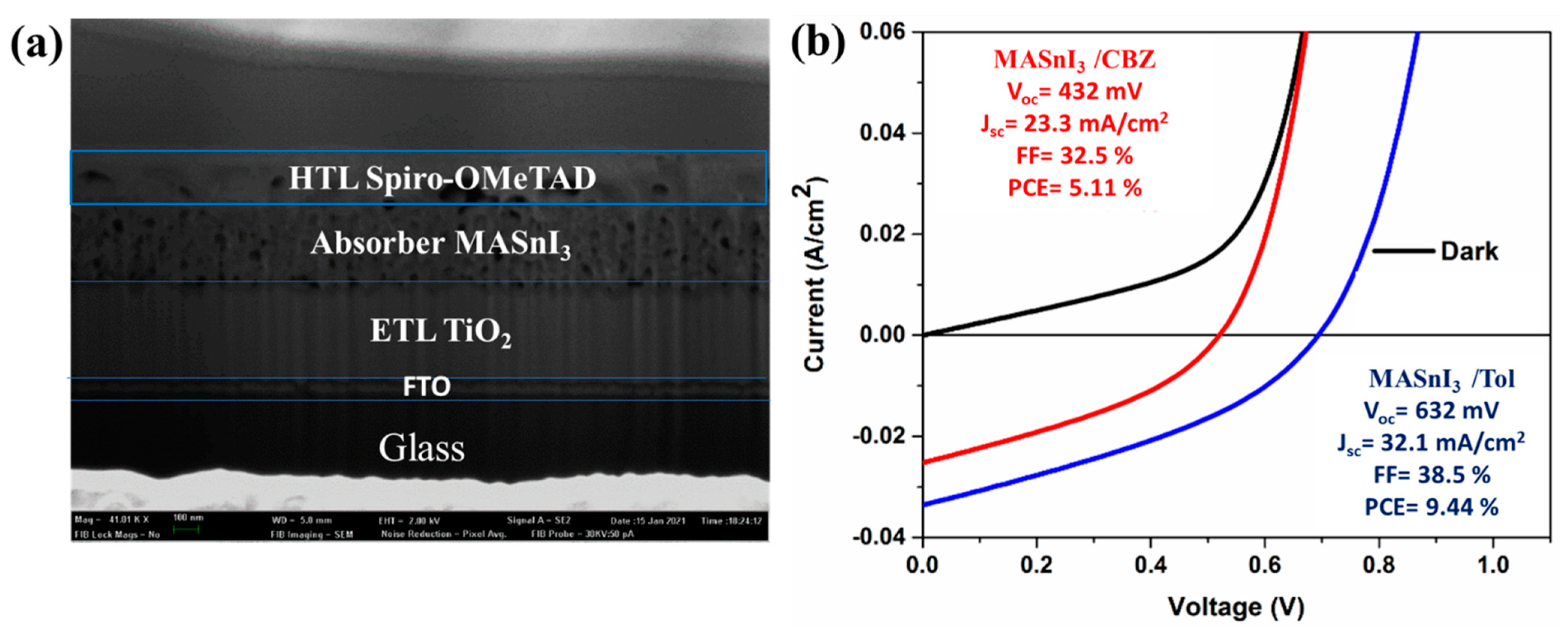
We then fabricated Gold/Spiro-OMeTAD/MASnI3/Compact-TiO2/FTO/Glass devices with MASnI3 films treated with toluene or chlorobenzene as antisolvents. We did not fabricate devices using MASnI3 films treated with diethyl ether because this antisolvent showed worse stability and morphology.
Figure 10 illustrates the photovoltaic performance of MASnI
3. The J–V curves showed that the prepared PSC realized a remarkable PCE improvement of 5.11% when using MASnI
3–chlorobenzene, an open-circuit voltage (V
oc) of 521.8 mV, a short-circuit current (J
sc) of 25.6 mA cm
−2, and a fill factor (FF) of 34.59%. PCE improvement was of 9.44% after treatment with toluene, using V
oc of 694.6 mV, J
sc of 32.1 mA cm
−2, and an FF of 38.09%, which was significantly higher than that measured for the MASnI
3–chlorobenzene-based solar cell. It is possible that the use of toluene increased the quality and stability of the film by increasing the carrier concentration and decreasing the electron–hole recombination, thus enhancing the photoconversion efficiency from 5.11% to 9.44%. A high value observed for J
sc is normally due to the exciting electrons generated following light absorption; the higher the light absorption, the higher the electron excitation, and as a resultant, J
SC will be high too [
33,
34]. Some results were not easy to reproduce because of the low-cost techniques used for the manufacture of the devices and because of variable temperature and humidity conditions in addition [
35,
36], some interface defects were noticed. Despite this, the results were generally quite reproducible with small differences. The obtained results might contribute to the production and commercialization of stable and efficient photovoltaic devices.
7. Conclusions
In this work, MASnI3 thin films were successfully prepared by the one-step spin coating technique. The effect of different antisolvents, i.e., diethyl ether, chlorobenzene, and toluene, on films’ properties was investigated using XRD, SEM, PL, and optical analyses.
The XRD analysis revealed that all samples had an extraordinary (110) peak intensity after treatment of the MASnI3 film. The XRD results showed that toluene led to superior crystallinity, reflected by the intensity of the (110) peak. This result was supported by SEM results, that showed that toluene led to increased grain size. Furthermore, the sample obtained with toluene treatment showed the highest absorbance. Our results suggest that using toluene to carry out the antisolvent quenching step in a one-step spin coating will lead to superior perovskite films and higher efficiencies of related devices. Using SCAPS-1D software, we also determined the effect of the three different antisolvents, i.e., diethyl ether, chlorobenzene, and toluene, on solar cell performance, obtaining the efficiencies of 9.93, 10.42, and 10.44%, respectively. We therefore conclude that toluene is the optimal antisolvent for the MASnI3 absorber layer. Additionally, we produced the device FTO/TiO2/MASnI3/Spiro-OMeTAD/Au, which showed a remarkable PCE of 9.11% when using a MASnI3 film treated with toluene.
Author Contributions
Data curation, J.M.-G.; Formal analysis, A.B.; Investigation, A.B. and B.M.S.; Methodology, A.B., B.M.S. and P.P.; Software, J.M.-G.; Supervision, B.M.S.; Validation, A.B. and P.P.; Writing—original draft, A.B. and J.M.-G.; Writing—review & editing, A.B., B.M.S. and P.P. All authors have read and agreed to the published version of the manuscript.
Funding
The author Amal Bouich postdoctoral researcher acknowledges Margarita Salas Fellowship (MCIN/AEI/10.13039/501100011033) for funding support. This work was supported by EU under Project PID2019-107137RB-C21 and by ERDF under the funding “A way of making Europe”. This work was supported by the Ministerio de Ciencia e Innvación through the project BESTMAT (PID2019-107137RB-C21) and (PID2019-107137RB-C22).
Institutional Review Board Statement
Not applicable.
Informed Consent Statement
Not applicable.
Data Availability Statement
All data is included in the manuscript.
Acknowledgments
We would like to thank Ministerio de Economía y Competitividad (Spain) for supporting this work and Margarita Salas Fellowship.
Conflicts of Interest
The authors declare that they have no known competing financial or personal interest.
References
- Green, M.A.; Emery, K.; Hishikawa, Y.; Warta, W.; Dunlop, E.D. Solar cell efficiency tables (Version 45). Prog. Photovolt. Res. Appl. 2015, 23, 1–9. [Google Scholar] [CrossRef]
- Jeon, N.J.; Na, H.; Jung, E.H.; Yang, T.-Y.; Lee, Y.G.; Kim, G.; Shin, H.-W.; Seok, S.I.; Lee, J.; Seo, J. A fluorene-terminated hole-transporting material for highly efficient and stable perovskite solar cells. Nat. Energy 2018, 3, 682–689. [Google Scholar] [CrossRef]
- Chu, Q.-Q.; Ding, B.; Qiu, Q.; Liu, Y.; Li, C.-X.; Li, C.-J.; Yang, G.-J.; Fang, B. Cost effective perovskite solar cells with a high efficiency and open-circuit voltage based on a perovskite-friendly carbon electrode. J. Mater. Chem. A 2018, 6, 8271–8279. [Google Scholar] [CrossRef]
- Chu, Q.-Q.; Cheng, B.; Fang, B. Interface passivation for perovskite solar cell: A good or bad strategy? Matter 2022, 5, 2444–2446. [Google Scholar] [CrossRef]
- Chu, Q.-Q.; Ding, B.; Li, Y.; Gao, L.; Qiu, Q.; Li, C.-X.; Li, C.-J.; Yang, G.-J.; Fang, B. Fast Drying Boosted Performance Improvement of Low-Temperature Paintable Carbon-Based Perovskite Solar Cell. ACS Sustain. Chem. Eng. 2017, 5, 9758–9765. [Google Scholar] [CrossRef]
- Bi, D.; Moon, S.-J.; Häggman, L.; Boschloo, G.; Yang, L.; Johansson, E.M.J.; Nazeeruddin, M.K.; Grätzel, M.; Hagfeldt, A. Using a two-step deposition technique to prepare perovskite (CH3NH3PbI3) for thin-film solar cells based on ZrO2 and TiO2 mesostructures. RSC Adv. 2013, 3, 18762–18766. [Google Scholar] [CrossRef]
- Chen, Q.; Zhou, H.; Hong, Z.; Luo, S.; Duan, H.-S.; Wang, H.-H.; Liu, Y.; Li, G.; Yang, Y. Planar Heterojunction Perovskite Solar Cells via Vapor-Assisted Solution Process. J. Am. Chem. Soc. 2013, 136, 622–625. [Google Scholar] [CrossRef]
- Leyden, M.R.; Ono, L.K.; Raga, S.R.; Kato, Y.; Wang, S.; Qi, Y. High performance perovskite solar cells by hybrid chemical vapor deposition. J. Mater. Chem. A 2014, 2, 18742–18745. [Google Scholar] [CrossRef]
- Paek, S.; Schouwink, P.; Athanasopoulou, E.N.; Cho, K.T.; Grancini, G.; Lee, Y.; Zhang, Y.; Stellacci, F.; Nazeeruddin, M.K.; Gao, P. From Nano- to Micrometer Scale: The Role of Antisolvent Treatment on High Performance Perovskite Solar Cells. Chem. Mater. 2017, 29, 3490–3498. [Google Scholar] [CrossRef]
- Taylor, A.D.; Sun, Q.; Goetz, K.P.; An, Q.; Schramm, T.; Hofstetter, Y.; Litterst, M.; Paulus, F.; Vaynzof, Y. A general approach to high-efficiency perovskite solar cells by any antisolvent. Nat. Commun. 2021, 12, 1878. [Google Scholar] [CrossRef]
- Ke, W.; Stoumpos, C.C.; Spanopoulos, I.; Mao, L.; Chen, M.; Wasielewski, M.R.; Kanatzidis, M.G. Efficient lead-free solar cells based on hollow {en}MASnI3 perovskites. J. Am. Chem. Soc. 2017, 139, 14800–14806. [Google Scholar] [CrossRef]
- Fujihara, T.; Terakawa, S.; Matsushima, T.; Qin, C.; Yahiro, M.; Adachi, C. Fabrication of high coverage MASnI3 perovskite films for stable, planar heterojunction solar cells. J. Mater. Chem. C. 2017, 5, 1121–1127. [Google Scholar] [CrossRef]
- Bouich, A.; Marí-Guaita, J.; Sahraoui, B.; Palacios, P.; Marí, B. Tetrabutylammonium (TBA)-Doped Methylammonium Lead Iodide: High Quality and Stable Perovskite Thin Films. Front. Energy Res. 2022, 10, 840817. [Google Scholar] [CrossRef]
- Gupta, S.; Cahen, D.; Hodes, G. How SnF2 Impacts the Material Properties of Lead-Free Tin Perovskites. J. Phys. Chem. C 2018, 122, 13926–13936. [Google Scholar] [CrossRef]
- Kong, W.; Ye, Z.; Qi, Z.; Zhang, B.; Wang, M.; Rahimi-Iman, A.; Wu, H. Characterization of an abnormal photoluminescence behavior upon crystal-phase transition of perovskite CH3NH3PbI3. Phys. Chem. Chem. Phys. 2015, 17, 16405–16411. [Google Scholar] [CrossRef]
- Guo, X.; McCleese, C.; Kolodziej, C.; Samia, A.C.; Zhao, Y.; Burda, C. Identification and characterization of the intermediate phase in hybrid organic-inorganic MAPbI3 perovskites. Dalton Trans. 2016, 45, 3806–3813. [Google Scholar] [CrossRef]
- Xiao, Z.; Dong, Q.; Bi, C.; Shao, Y.; Yuan, Y.; Huang, J. Solvent Annealing of Perovskite-Induced Crystal Growth for Photovoltaic-Device Efficiency Enhancement. Adv. Mater. 2014, 26, 6503–6509. [Google Scholar] [CrossRef]
- Luo, S.; Daoud, W.A. Crystal Structure Formation of CH3NH3PbI3−xClx Perovskite. Materials 2016, 9, 123. [Google Scholar] [CrossRef]
- Park, N.-G. Crystal growth engineering for high efficiency perovskite solar cells. CrystEngComm. 2016, 18, 5977–5985. [Google Scholar] [CrossRef]
- Zheng, X.; Chen, B.; Wu, C.; Priya, S. Room temperature fabrication of CH3NH3PbBr3 by anti-solvent assisted crystallization approach for perovskite solar cells with fast response and small J–V hysteresis. Nano Energy 2015, 17, 269–278. [Google Scholar] [CrossRef]
- Slotcavage, D.J.; Karunadasa, H.I.; McGehee, M.D. Light-Induced Phase Segregation in Halide-Perovskite Absorbers. ACS Energy Lett. 2016, 1, 1199–1205. [Google Scholar] [CrossRef]
- Jeangros, Q.; Duchamp, M.; Werner, J.; Kruth, M.; Dunin-Borkowski, R.E.; Niesen, B.; Ballif, C.; Hessler-Wyser, A. In Situ TEM Analysis of Organic–Inorganic Metal-Halide Perovskite Solar Cells under Electrical Bias. Nano Lett. 2016, 16, 7013–7018. [Google Scholar] [CrossRef] [PubMed]
- Liu, D.; Yang, J.; Kelly, T.L. Compact layer-free perovskite solar cells with 13.5% efficiency. J. Am. Chem. Soc. 2014, 136, 17116–17122. [Google Scholar] [CrossRef] [PubMed]
- Zhang, M.; Yu, H.; Lyu, M.; Wang, Q.; Yun, J.H.; Wang, L. Composition-dependent photoluminescence intensity and prolonged recombination lifetime of perovskite CH3NH3PbBr3−xClx films. Chem. Commun. 2014, 50, 11727–11730. [Google Scholar] [CrossRef]
- Choi, J.J.; Yang, X.; Norman, Z.M.; Billinge, S.J.L.; Owen, J.S. Structure of Methylammonium Lead Iodide Within Mesoporous Titanium Dioxide: Active Material in High-Performance Perovskite Solar Cells. Nano Lett. 2013, 14, 127–133. [Google Scholar] [CrossRef]
- Halder, A.; Chulliyil, R.; Subbiah, A.S.; Khan, T.; Chattoraj, S.; Chowdhury, A.; Sarkar, S.K. Pseudohalide (SCN–)-doped MAPbI3 perovskites: A few surprises. J. Phys. Chem. Lett. 2015, 6, 3483–3489. [Google Scholar] [CrossRef]
- Wang, F.; Ma, J.; Xie, F.; Li, L.; Chen, J.; Fan, J.; Zhao, N. Organic Cation-Dependent Degradation Mechanism of Organotin Halide Perovskites. Adv. Funct. Mater. 2016, 26, 3417–3423. [Google Scholar] [CrossRef]
- Nishikubo, R.; Ishida, N.; Katsuki, Y.; Wakamiya, A.; Saeki, A. Minute-scale degradation and shift of valence-band maxima of (CH3NH3)SnI3 and HC(NH2)2SnI3 perovskites upon air exposure. J. Phys. Chem. C 2017, 121, 19650–19656. [Google Scholar] [CrossRef]
- Marí-Guaita, J.; Bouich, A.; Marí, B. Shedding Light on Phase Stability and Surface Engineering of Formamidinium Lead Iodide (FaPbI3) Thin Films for Solar Cells. Eng. Proc. 2021, 12, 1. [Google Scholar]
- Malinauskas, T.; Tomkute-Luksiene, D.; Sens, R.; Daskeviciene, M.; Send, R.; Wonneberger, H.; Jankauskas, V.; Bruder, I.; Getautis, V. Enhancing thermal stability and lifetime of solid-state dye-sensitized solar cells via molecular engineering of the hole-transporting material spiro-OMeTAD. ACS Appl. Mater. Interfaces 2015, 7, 11107–11116. [Google Scholar] [CrossRef]
- Zhang, J.-Y.; Boyd, I.; O’Sullivan, B.; Hurley, P.; Kelly, P.; Sénateur, J.-P. Nanocrystalline TiO2 films studied by optical, XRD and FTIR spectroscopy. J. Non-Cryst. Solids 2002, 303, 134–138. [Google Scholar] [CrossRef]
- Hasan, M.M.; Haseeb, A.S.M.A.; Saidur, R.; Masjuki, H.H. Effects of annealing treatment on optical properties of anatase TiO2 thin films. Int. J. Chem. Biol. Eng. 2008, 1, 92–96. [Google Scholar]
- Zhang, L.; Pan, Z.; Wang, W.; Du, J.; Ren, Z.; Shen, Q.; Zhong, X. Copper deficient Zn–Cu–In–Se quantum dot sensitized solar cells for high efficiency. J. Mater. Chem. A 2017, 5, 21442–21451. [Google Scholar] [CrossRef]
- Koo, H.-J.; Kim, Y.J.; Lee, Y.H.; Lee, W.I.; Kim, K.; Park, N.-G. Nano-embossed Hollow Spherical TiO2 as Bifunctional Material for High-Efficiency Dye-Sensitized Solar Cells. Adv. Mater. 2008, 20, 195–199. [Google Scholar] [CrossRef]
- Doumbia, Y.; Bouich, A.; Soro, D.; Soucase, B.M. Mixed halide head perovskites thin films: Stability and growth investigation. Optik 2022, 261, 169222. [Google Scholar] [CrossRef]
- Fradi, K.; Bouich, A.; Slimi, B.; Chtourou, R. Towards improving the optoelectronics properties of MAPbI3(1−x)B3x/ZnO heterojunction by bromine doping. Optik 2022, 249, 168283. [Google Scholar] [CrossRef]
Figure 1.
(a) XRD patterns of MASnI3 films treated with toluene, chlorobenzene, and diethyl ether (b) FWHM of MASnI3 films treated with toluene, chlorobenzene, and diethyl ether.
Figure 1.
(a) XRD patterns of MASnI3 films treated with toluene, chlorobenzene, and diethyl ether (b) FWHM of MASnI3 films treated with toluene, chlorobenzene, and diethyl ether.
Figure 2.
SEM images of MASnI3 films treated with (a) diethyl ether, (b) toluene, (c) chlorobenzene.
Figure 2.
SEM images of MASnI3 films treated with (a) diethyl ether, (b) toluene, (c) chlorobenzene.
Figure 3.
(a) Absorption of MASnI3 films, (b) bandgap, and (c) PL spectra after treatment with toluene, diethyl ether, and chlorobenzene, (d) structure of MASnI3.
Figure 3.
(a) Absorption of MASnI3 films, (b) bandgap, and (c) PL spectra after treatment with toluene, diethyl ether, and chlorobenzene, (d) structure of MASnI3.
Figure 4.
Degradation study of MASnI3 films treated with different antisolvents. (a) XRD pattern of fresh and four-week-old MASnI3 films treated with toluene, (b) XRD pattern of fresh and four-week-old MASnI3 films treated with diethyl ether, (c) XRD pattern of fresh and aged MASnI3 films treated with chlorobenzene, (d) SEM image of an aged MASnI3 film treated with toluene, (e) SEM image of a four-week-old MASnI3 film treated with diethyl ether (f) SEM image of a four-week-old MASnI3 film treated with chlorobenzene.
Figure 5.
Schematic of a MASnI3-based solar cell structure.
Figure 5.
Schematic of a MASnI3-based solar cell structure.
Figure 6.
(a) J–V and (b) P–V characteristics curves of MASnI3-based solar cell.
Figure 6.
(a) J–V and (b) P–V characteristics curves of MASnI3-based solar cell.
Figure 7.
Characteristic parameters of a MASnI3-based solar cell when using the different antisolvents.
Figure 7.
Characteristic parameters of a MASnI3-based solar cell when using the different antisolvents.
Figure 8.
(a) XRD Pattern of the Spiro-OmeTAD film, (b) bandgap spectra of the Spiro-OmeTAD film, (c) XRD pattern of the TiO2 compact layer, (d) bandgap spectra of the TiO2 compact layer. “3.5E+12” represents “3.5 × 10¹²”, same applies to other E notations in the figure.
Figure 8.
(a) XRD Pattern of the Spiro-OmeTAD film, (b) bandgap spectra of the Spiro-OmeTAD film, (c) XRD pattern of the TiO2 compact layer, (d) bandgap spectra of the TiO2 compact layer. “3.5E+12” represents “3.5 × 10¹²”, same applies to other E notations in the figure.
Figure 9.
(a) SEM image of the Spiro-OMeTAD film, (b) SEM image of the TiO2 compact layer.
Figure 9.
(a) SEM image of the Spiro-OMeTAD film, (b) SEM image of the TiO2 compact layer.
Figure 10.
(a) Cross section of a lead-free perovskite solar cell. (b) I–V performance of perovskite MASnI3 (black color = dark curves are identical for both devices, Red color = chlorobenzene, Blue color = toluene) (b) cross-section of a lead-free perovskite solar cell.
Figure 10.
(a) Cross section of a lead-free perovskite solar cell. (b) I–V performance of perovskite MASnI3 (black color = dark curves are identical for both devices, Red color = chlorobenzene, Blue color = toluene) (b) cross-section of a lead-free perovskite solar cell.
Table 1.
Parameters of XRD spectra of MASnI3 films treated with toluene, chlorobenzene, and diethyl ether.
Table 1.
Parameters of XRD spectra of MASnI3 films treated with toluene, chlorobenzene, and diethyl ether.
| Sample ID | Grain Size (nm) | Dislocation Density (nm−1) | Lattice Strain (ԑ) |
|---|
| MASnI3-ET | 340 | 1.05 × 10⁻⁵ | 0.38 |
| MASnI3-CBZ | 360 | 0.90 × 10⁻⁵ | 0.39 |
| MASnI3-Tol | 400 | 0.62 × 10⁻⁵ | 0.37 |
Table 2.
Optical bandgaps of the MASnI3 samples treated with toluene, diethyl ether, and chlorobenzene.
Table 2.
Optical bandgaps of the MASnI3 samples treated with toluene, diethyl ether, and chlorobenzene.
| Sample | λ (nm) | Eg from PL (eV) | λ (nm) | Eg from UV (eV) | Stokes Shift (meV) |
|---|
| MASnI3-ET | 779 | 1.59 | 750 | 1.63 | 40 |
| MASnI3-TOL | 782 | 1.58 | 759 | 1.60 | 20 |
| MASnI3-CBZ | 787 | 1.57 | 760 | 1.62 | 50 |
Table 3.
Bandgap variation for MASnI3 calculated from the UV–visible spectra, using diethyl ether, toluene, and chlorobenzene.
Table 3.
Bandgap variation for MASnI3 calculated from the UV–visible spectra, using diethyl ether, toluene, and chlorobenzene.
| Sample | Thickness (nm) | Band Gap-UV (eV) |
|---|
| MASnI3-ET | 200 | 1.63 |
| MASnI3-TOL | 210 | 1.60 |
| MASnI3-CBZ | 210 | 1.62 |
Table 4.
Experimental Characteristics Parameters MASnI3-based solar cell.
Table 4.
Experimental Characteristics Parameters MASnI3-based solar cell.
| Solar Cell Model | Voc | Jsc | FF | Eta |
|---|
| V | mA/cm2 | % | % |
|---|
| Spiro-OMeTAD/MASnI3: ET/TiO2/FTO | 0.94 | 12.49 | 84.29 | 9.93 |
| Spiro-OMeTAD/MASnI3: TOL/TiO2/FTO | 0.90 | 13.69 | 84.01 | 10.44 |
| Spiro-OMeTAD/MASnI3: CBZ/TiO2/FTO | 0.88 | 14.02 | 83.72 | 10.42 |
Table 5.
Average performance of the Spiro-OMeTAD/MASnI3/C-TiO2/FTO devices.
Table 5.
Average performance of the Spiro-OMeTAD/MASnI3/C-TiO2/FTO devices.
| Device. ID | Size | | FF | | |
|---|
| [cm2] | [%] | [%] | [V] | [mA/cm2] |
|---|
| S1-TOL | 0.1 | 9.44 | 38.09 | 0.69 | 32.01 |
| S2-TOL | 0.1 | 8.31 | 37.07 | 0.60 | 29.21 |
| S3-CBZ | 0.1 | 5.11 | 34.59 | 0.52 | 25.60 |
| S4-CBZ | 0.1 | 4.26 | 33.62 | 0.51 | 24.25 |
| Publisher’s Note: MDPI stays neutral with regard to jurisdictional claims in published maps and institutional affiliations. |
© 2022 by the authors. Licensee MDPI, Basel, Switzerland. This article is an open access article distributed under the terms and conditions of the Creative Commons Attribution (CC BY) license (https://creativecommons.org/licenses/by/4.0/).


