

Investigation of the Surface Coating, Humidity Degradation, and Recovery of Perovskite Film Phase for Solar-Cell Applications

 ,
, 

 ,
, 
Abstract
:1. Introduction
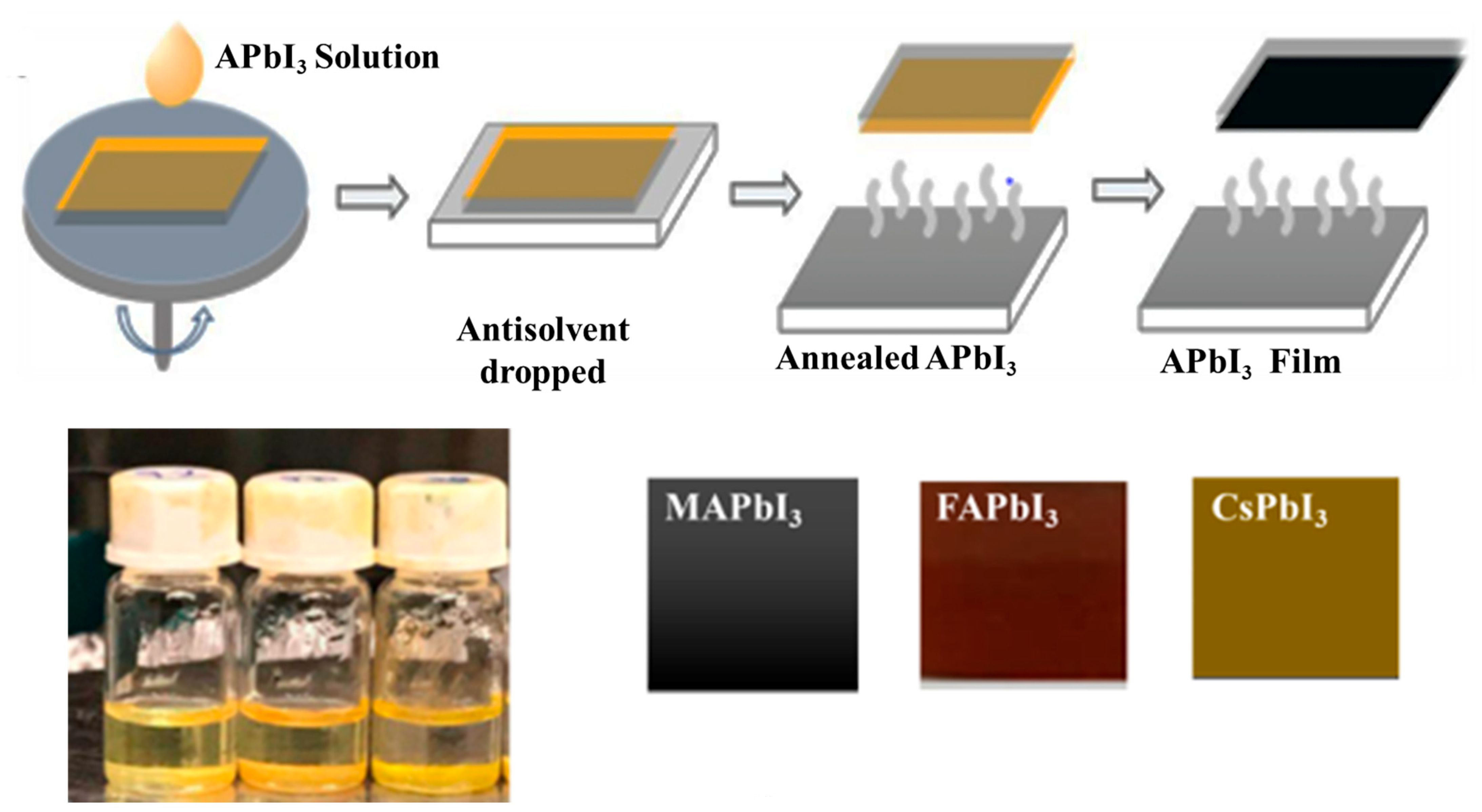
2. Thin-Film Manufacture
2.1. Experimental Procedure
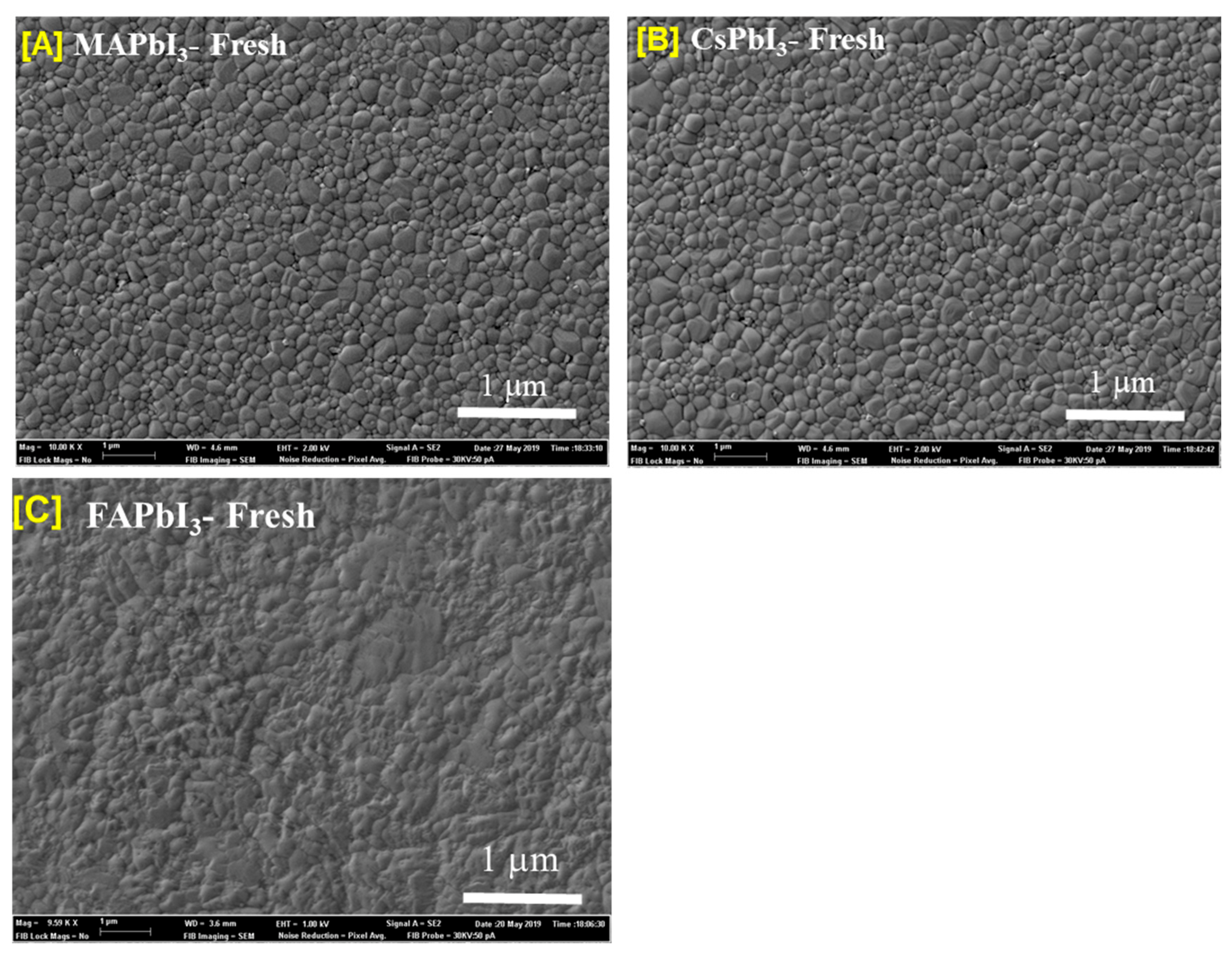
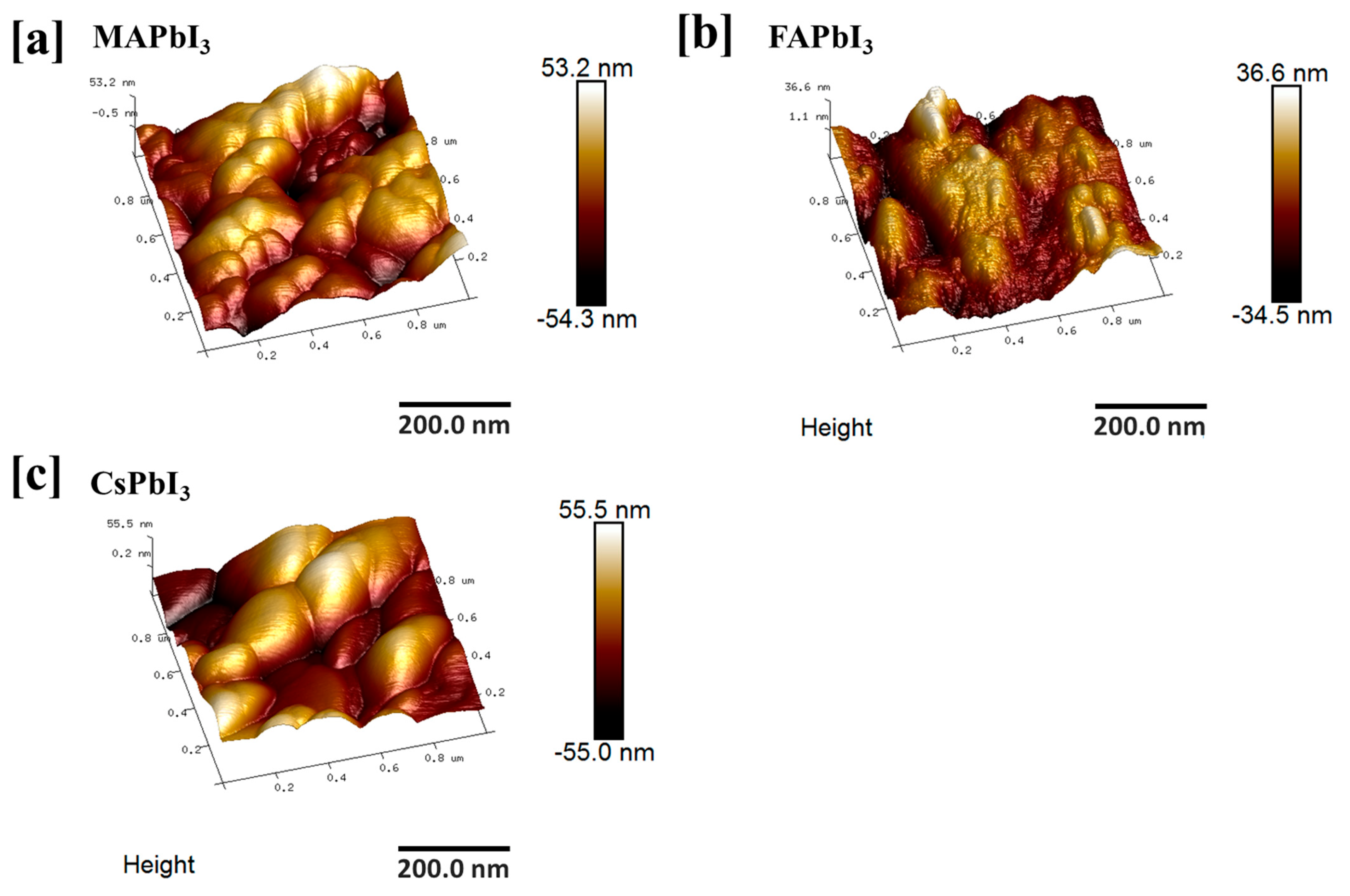
2.2. Film Characterization
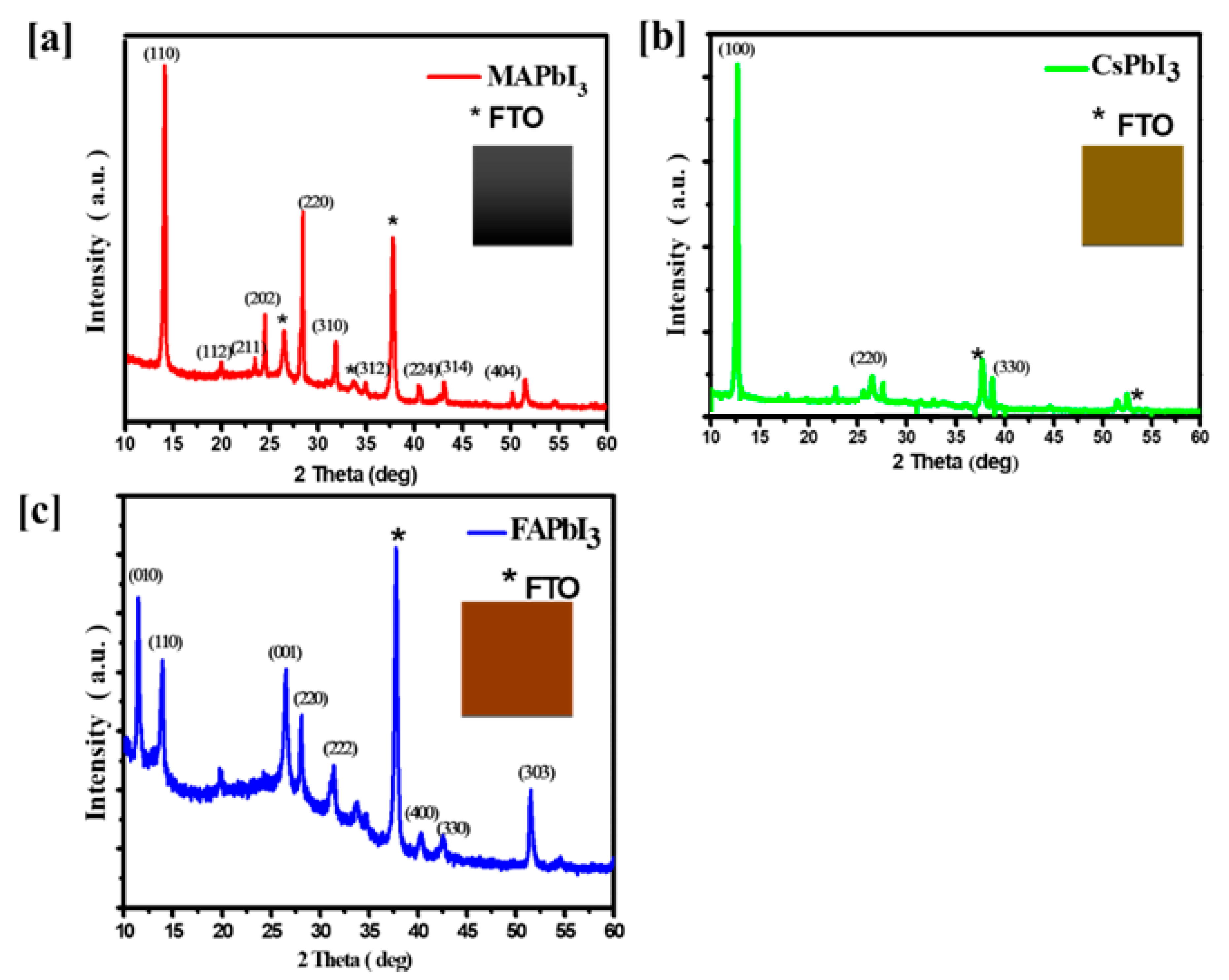
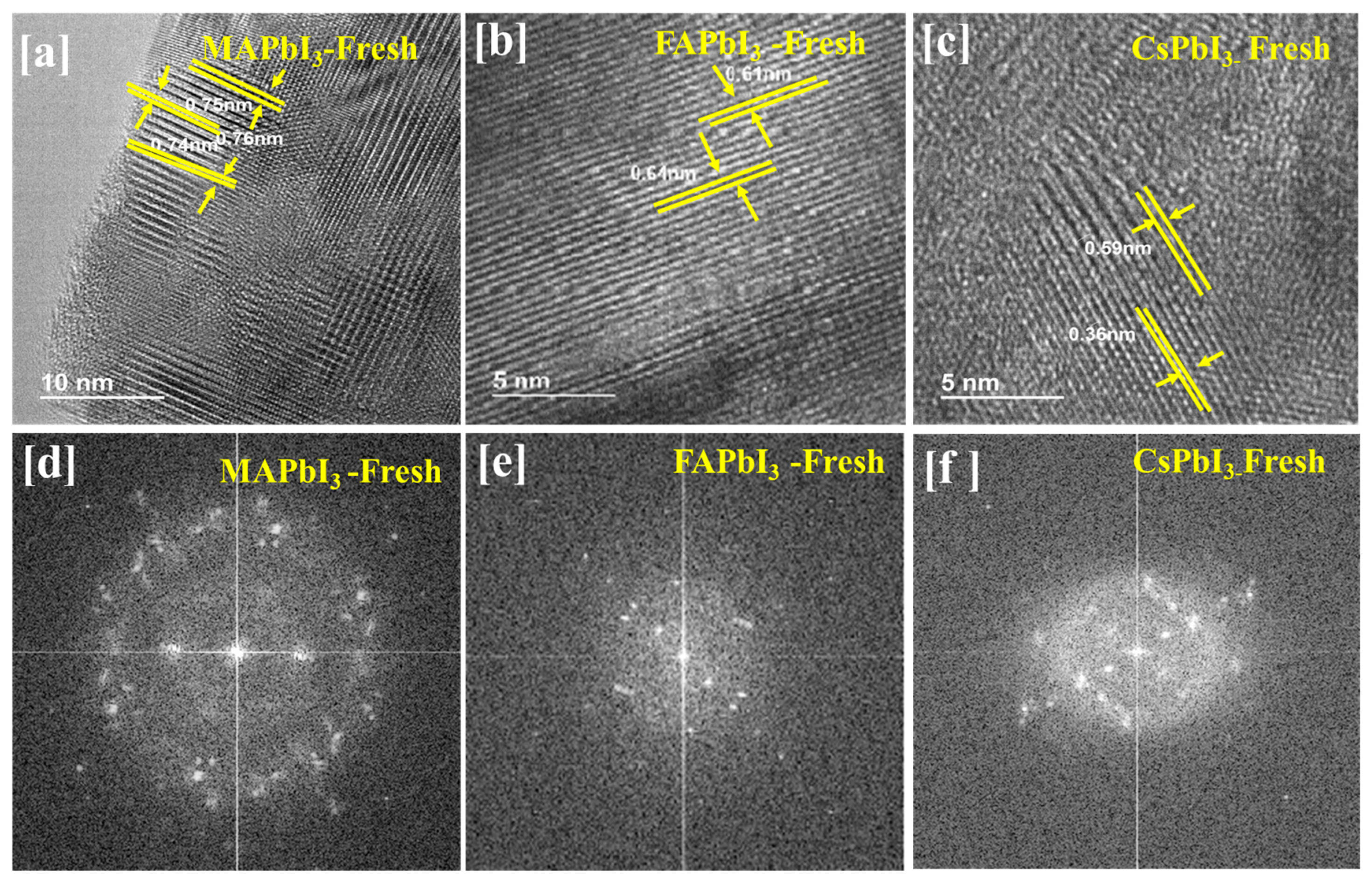
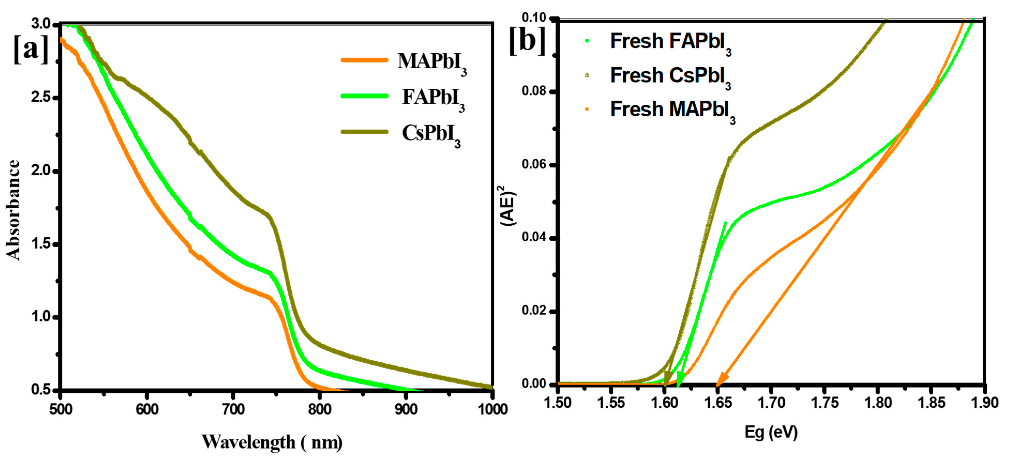
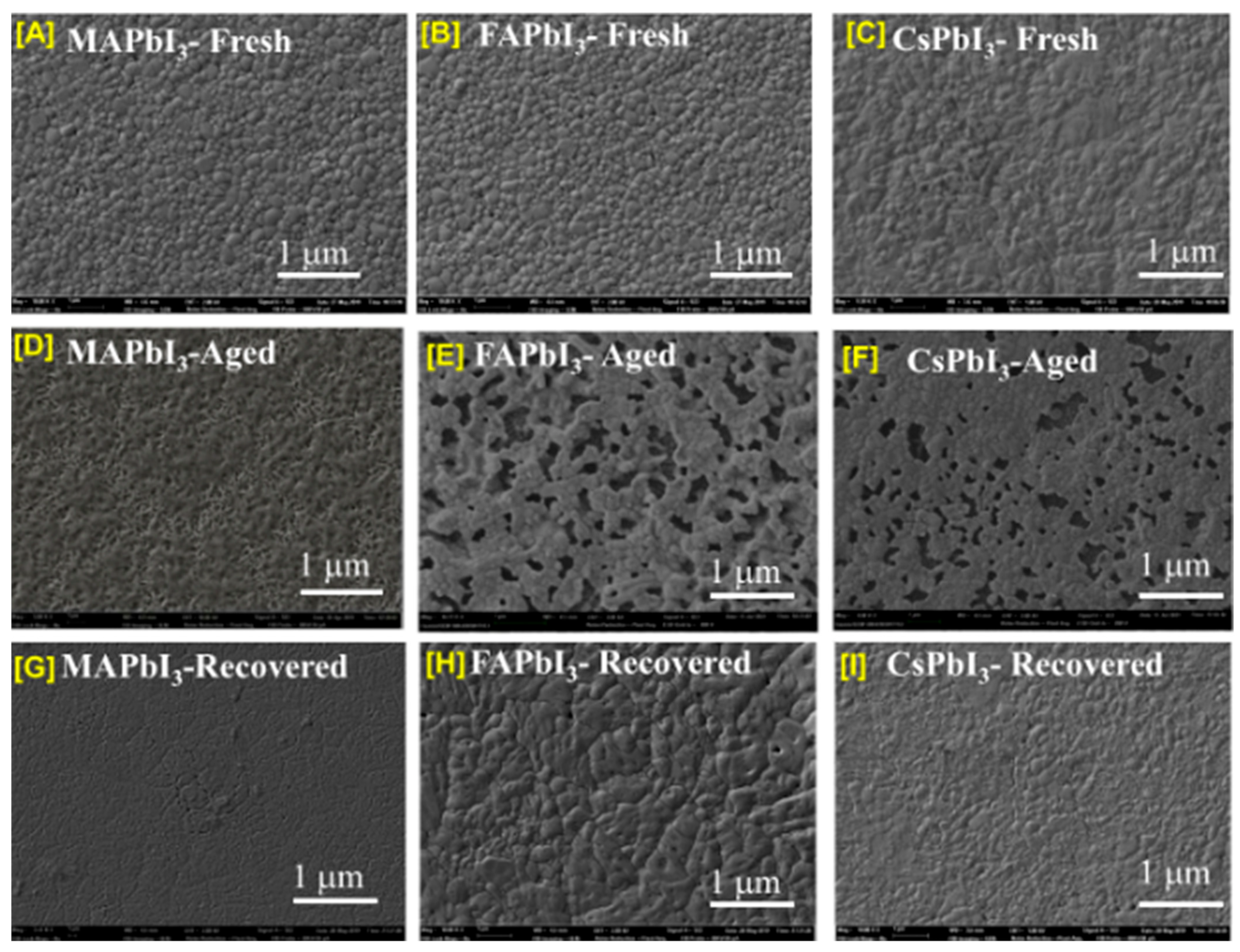
3. Results and Discussion
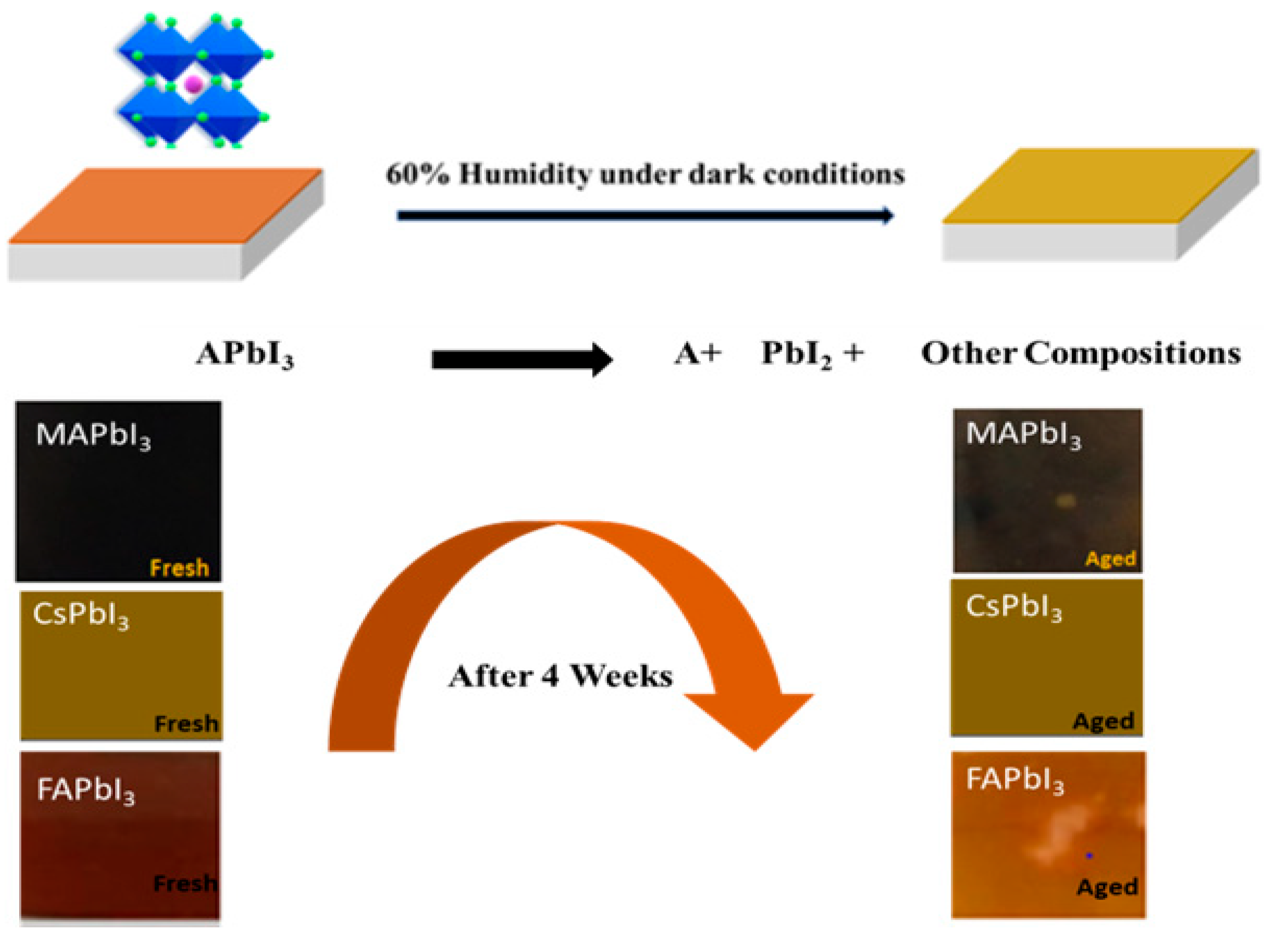
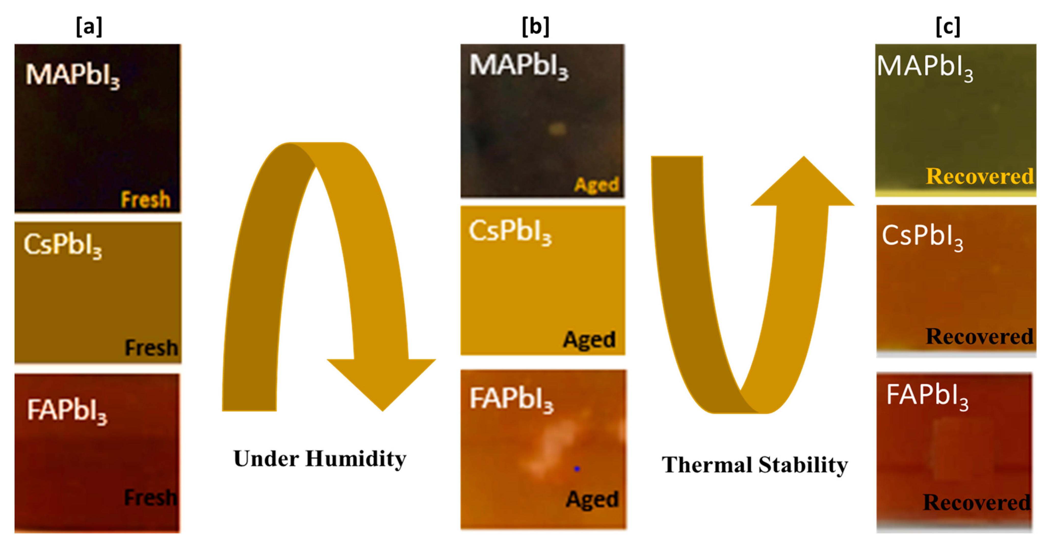
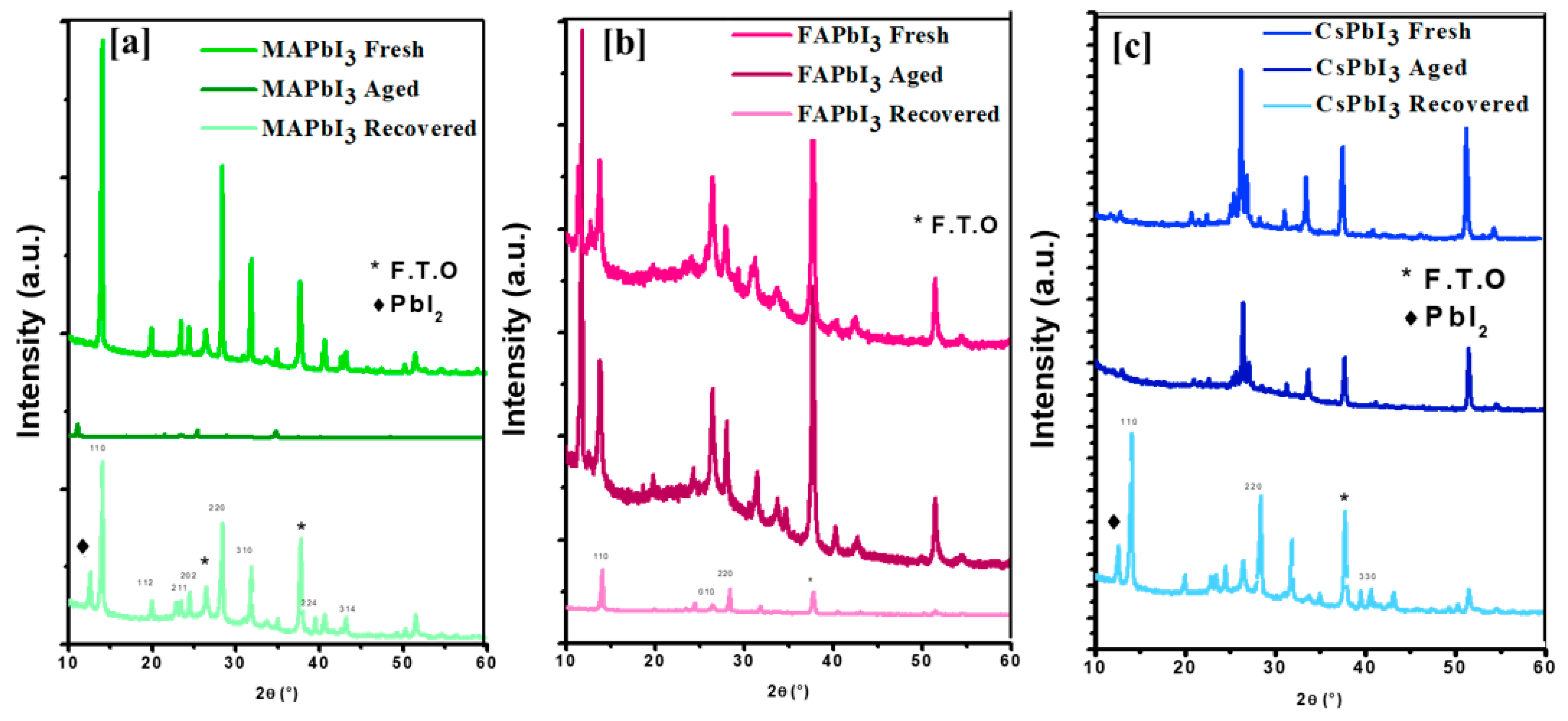
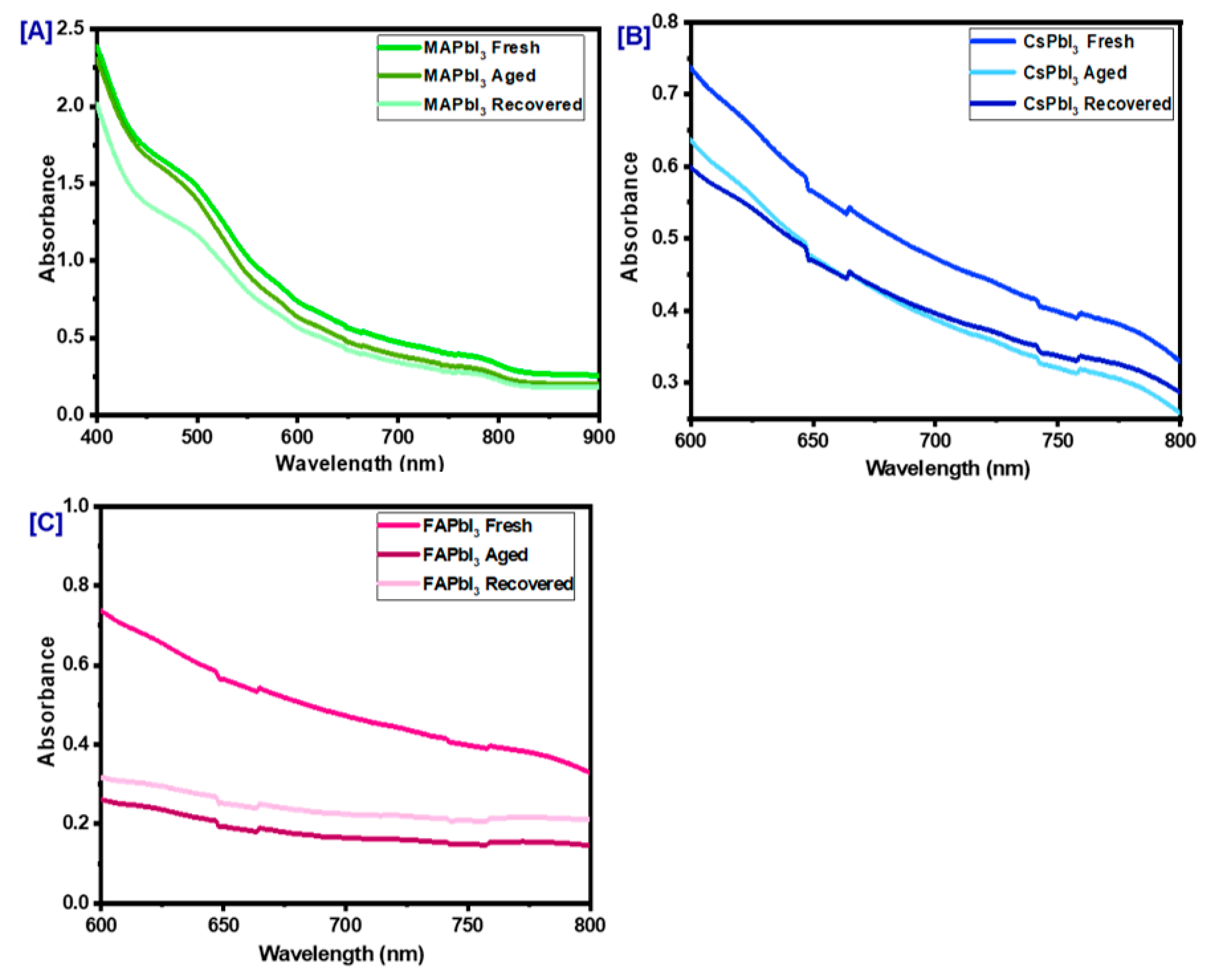
4. Degradation Study
5. Film Recovering
6. Numerical Analysis
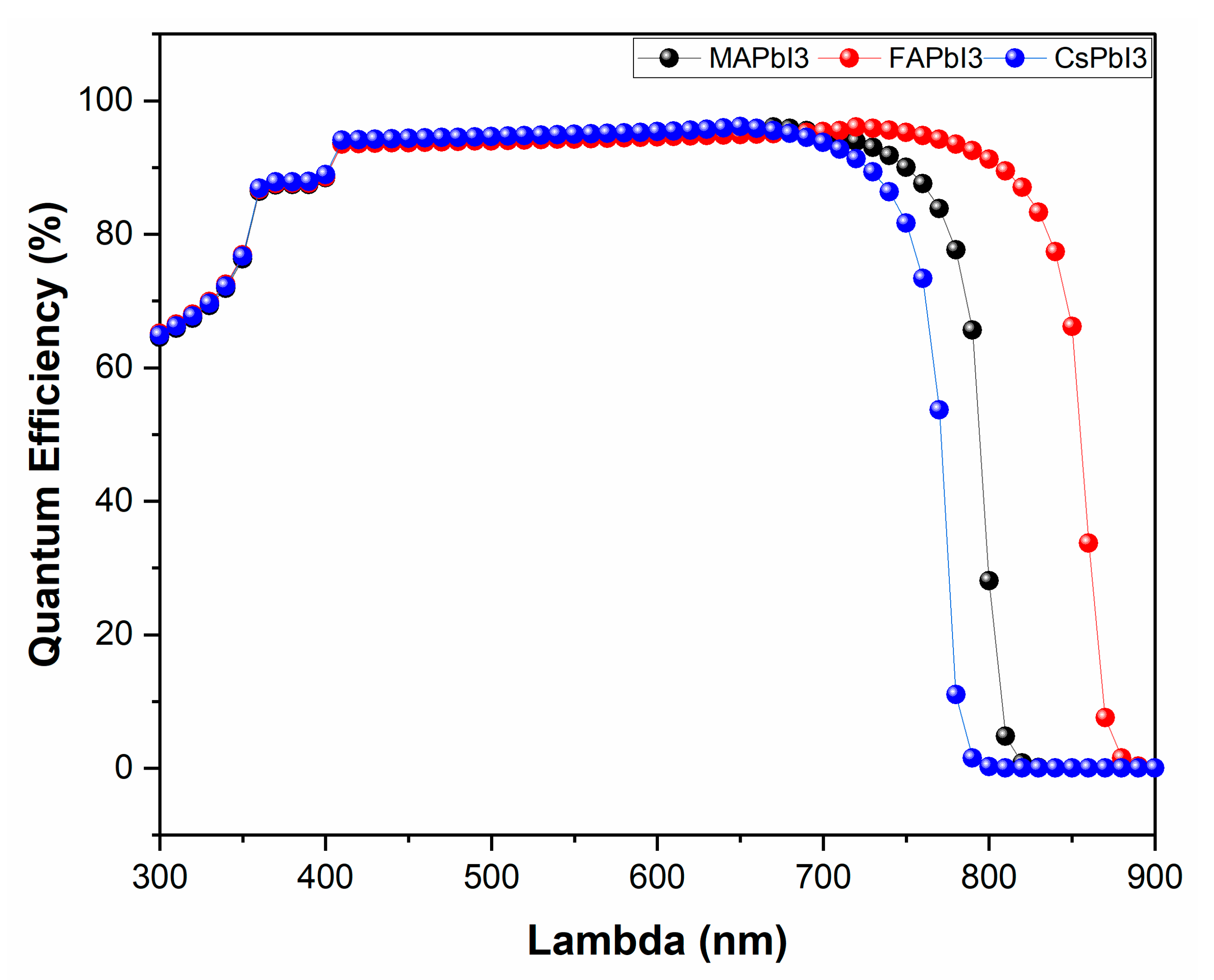
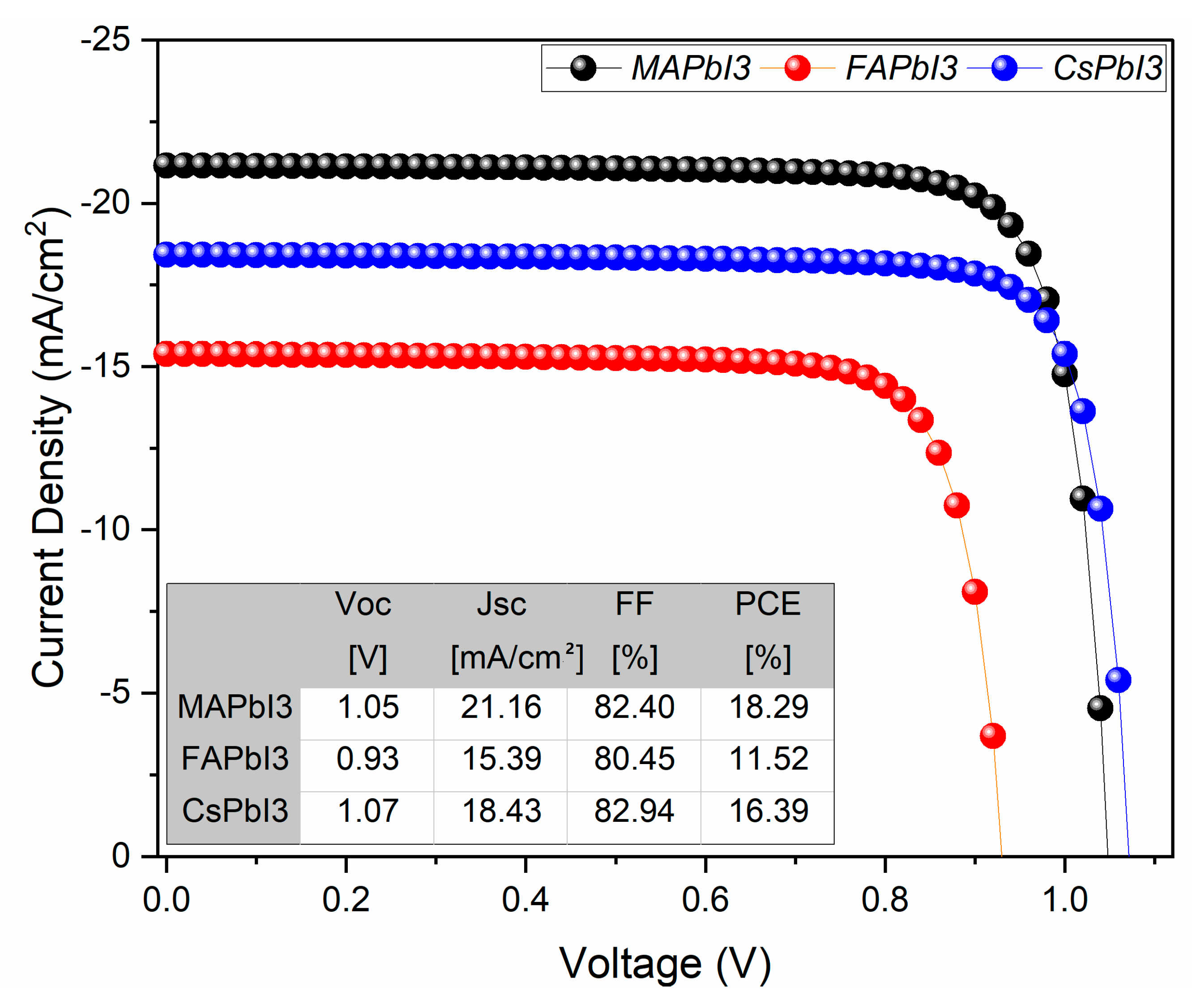
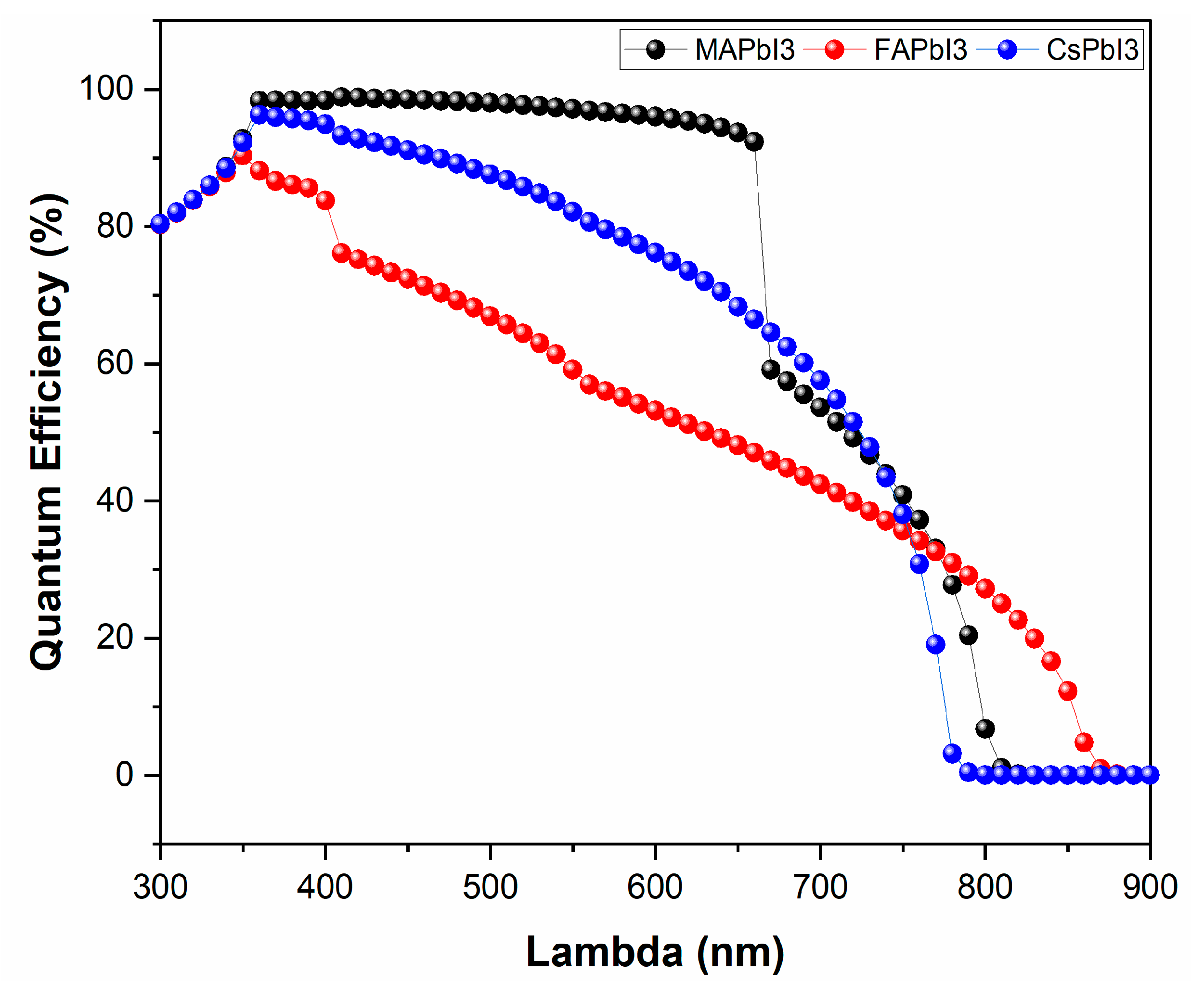
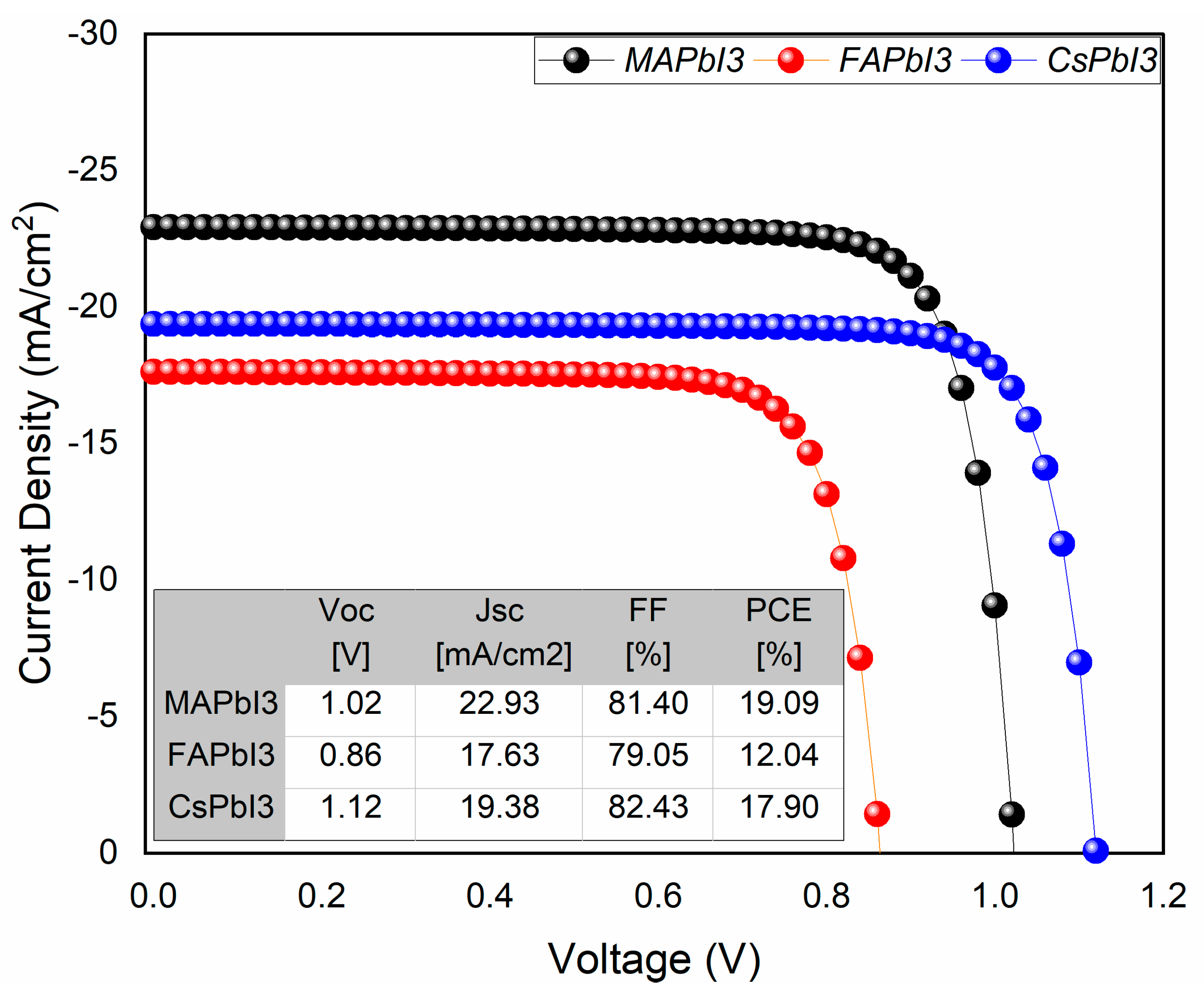
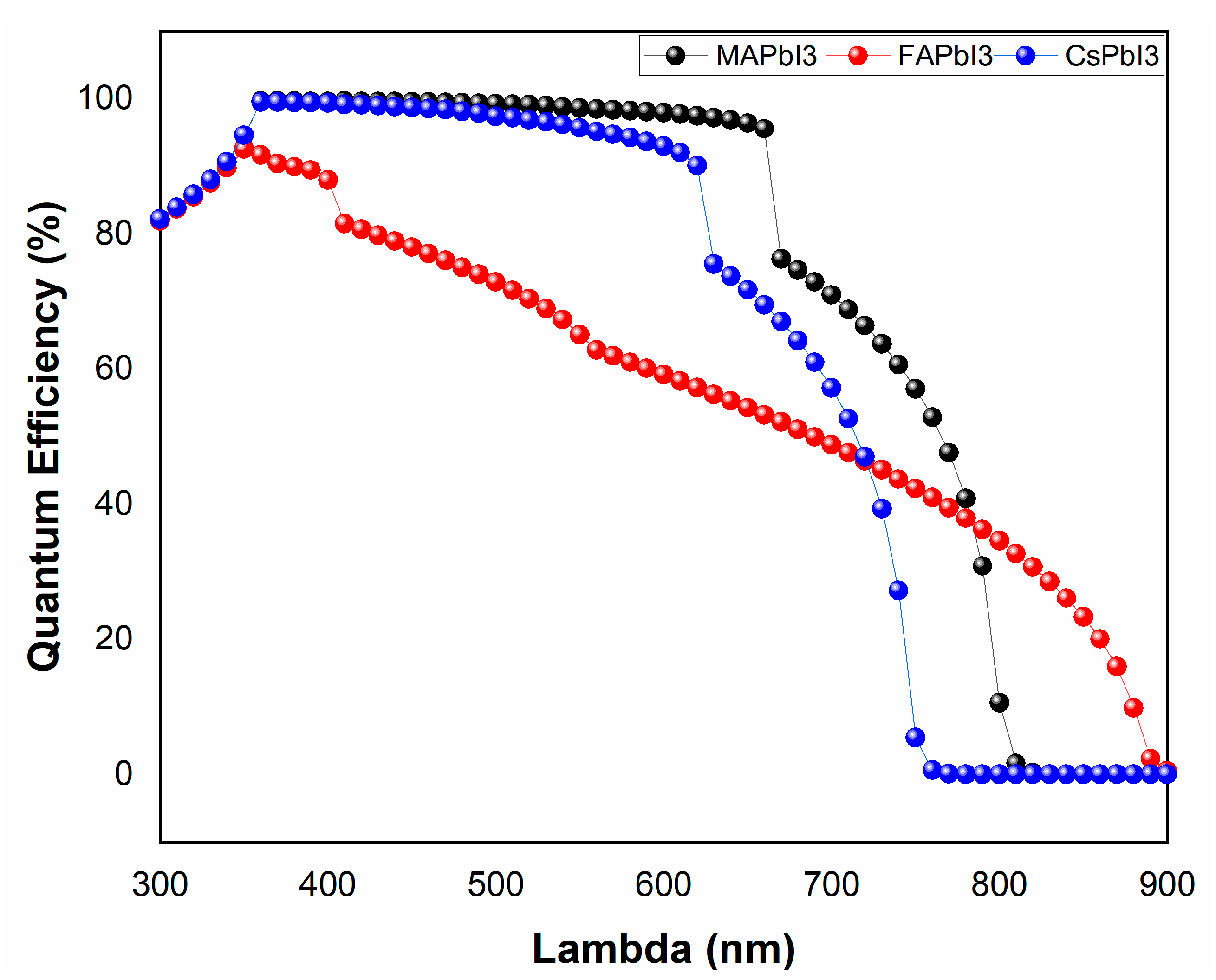
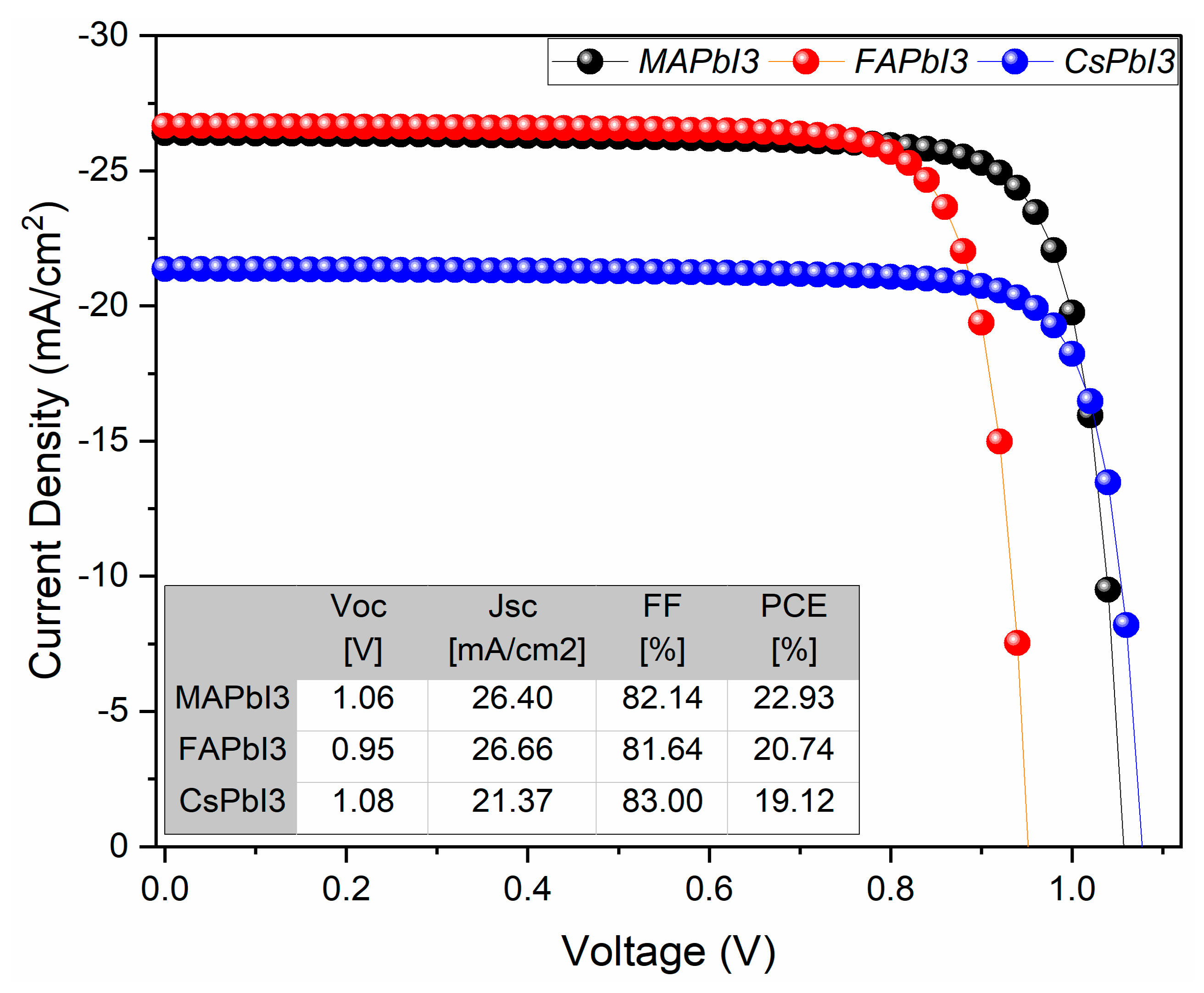
- JV and QE% as deposited.
- JV and QE% after degradation.
- JV and QE% after recovery.
7. Conclusions
Author Contributions
Funding
Institutional Review Board Statement
Informed Consent Statement
Data Availability Statement
Acknowledgments
Conflicts of Interest
References
- Lakhdar, N.; Hima, A. Electron transport material effect on performance of perovskite solar cells based on CH3NH3GeI3. Opt. Mater. 2019, 99, 109517. [Google Scholar] [CrossRef]
- Bouich, A.; Mari, B.; Atourki, L.; Ullah, S.; Touhami, M.E. Shedding light on the effect of diethyl ether antisolvent on the growth of (CH3NH3) PbI3 thin films. JOM 2021, 73, 551–557. [Google Scholar] [CrossRef]
- Rai, S.; Pandey, B.K.; Dwivedi, D.K. Modeling of highly efficient and low cost CH3NH3Pb(I1-xClx)3 based perovskite solar cell by numerical simulation. Opt. Mater. 2019, 100, 109631. [Google Scholar] [CrossRef]
- Khattak, Y.H.; Vega, E.; Baig, F.; Soucase, B.M. Performance investigation of experimentally fabricated lead iodide perovskite solar cell via numerical analysis. Mater. Res. Bull. 2022, 151, 111802. [Google Scholar] [CrossRef]
- Ma, T.; Wang, S.; Zhang, Y.; Zhang, K.; Yi, L. The development of all-inorganic CsPbX3 perovskite solar cells. J. Mater. Sci. 2019, 55, 464–479. [Google Scholar] [CrossRef]
- Ding, M.; Sun, L.; Chen, X.; Luo, T.; Ye, T.; Zhao, C.; Zhang, W.; Chang, H. Air-processed, large grain perovskite films with low trap density from perovskite crystal engineering for high-performance perovskite solar cells with improved ambient stability. J. Mater. Sci. 2019, 54, 12000–12011. [Google Scholar] [CrossRef]
- Hu, R.; Hou, W.; Han, G.; Ou, T.; Chang, Y.; Xiao, Y. Interfacial chemical bridge constructed by l-cysteine for highly efficient perovskite solar cells. Mater. Res. Bull. 2021, 149, 111698. [Google Scholar] [CrossRef]
- Khattak, Y.H.; Baig, F.; Shuja, A.; Beg, S.; Soucase, B.M. Numerical analysis guidelines for the design of efficient novel nip structures for perovskite solar cell. Sol. Energy 2020, 207, 579–591. [Google Scholar] [CrossRef]
- Kojima, A.; Teshima, K.; Shirai, Y.; Miyasaka, T. Organometal Halide Perovskites as Visible-Light Sensitizers for Photovoltaic Cells. J. Am. Chem. Soc. 2009, 131, 6050–6051. [Google Scholar] [CrossRef]
- Basumatary, P.; Agarwal, P. A short review on progress in perovskite solar cells. Mater. Res. Bull. 2022, 149, 111700. [Google Scholar] [CrossRef]
- Im, J.-H.; Lee, C.-R.; Lee, J.-W.; Park, S.-W.; Park, N.-G. 6.5% efficient perovskite quantum-dot-sensitized solar cell. Nanoscale 2011, 3, 4088–4093. [Google Scholar] [CrossRef] [PubMed]
- Kim, H.-S.; Lee, C.-R.; Im, J.-H.; Lee, K.-B.; Moehl, T.; Marchioro, A.; Moon, S.-J.; Humphry-Baker, R.; Yum, J.-H.; Moser, J.E.; et al. Lead Iodide Perovskite Sensitized All-Solid-State Submicron Thin Film Mesoscopic Solar Cell with Efficiency Exceeding 9%. Sci. Rep. 2012, 2, 591. [Google Scholar] [CrossRef] [PubMed]
- Doumbia, Y.; Bouich, A.; Soro, D.; Soucase, B.M. Mixed halide head perovskites thin films: Stability and growth investigation. Optik 2022, 261, 169222. [Google Scholar] [CrossRef]
- Yalçin, L.; Öztürk, R. Performance comparison of c-Si, mc-Si and a-Si thin film PV by PVsyst simulation. J. Optoelectron. Adv. Mater. 2013, 15, 326–334. [Google Scholar]
- Devi, C.; Mehra, R. Device simulation of lead-free MASnI3 solar cell with CuSbS2 (copper antimony sulfide). J. Mater. Sci. 2019, 54, 5615–5624. [Google Scholar] [CrossRef]
- Stoumpos, C.C.; Malliakas, C.D.; Kanatzidis, M.G. Semiconducting Tin and Lead Iodide Perovskites with Organic Cations: Phase Transitions, High Mobilities, and Near-Infrared Photoluminescent Properties. Inorg. Chem. 2013, 52, 9019–9038. [Google Scholar] [CrossRef] [PubMed]
- Green, M.A.; Emery, K.; King, D.L.; Igari, S.; Warta, W. Solar cell efficiency tables (Version 55). Prog. Photovoltaics Res. Appl. 2020, 28, 3–15. [Google Scholar] [CrossRef]
- Yoshikawa, K.; Kawasaki, H.; Yoshida, W.; Irie, T.; Konishi, K.; Nakano, K.; Uto, T.; Adachi, D.; Kanematsu, M.; Uzu, H.; et al. Silicon heterojunction solar cell with interdigitated back contacts for a photoconversion efficiency over 26%. Nat. Energy 2017, 2, 17032. [Google Scholar] [CrossRef]
- Chowdhury, M.S.; Shahahmadi, S.; Chelvanathan, P.; Tiong, S.; Amin, N.; Techato, K.; Nuthammachot, N.; Chowdhury, T.; Suklueng, M. Effect of deep-level defect density of the absorber layer and n/i interface in perovskite solar cells by SCAPS-1D. Results Phys. 2020, 16, 102839. [Google Scholar] [CrossRef]
- Chen, P.; Wang, E.; Yin, X.; Xie, H.; Que, M.; Liu, J.; Gao, B.; Que, W. Highly efficient and reproducible planar perovskite solar cells with mitigated hysteresis enabled by sequential surface modification of electrodes. J. Mater. Sci. 2018, 53, 16062–16073. [Google Scholar] [CrossRef]
- Zhang, J.; Tan, C.H.; Du, T.; Morbidoni, M.; Lin, C.T.; Xu, S.; Durrant, J.R.; McLachlana, M.A. ZnO-PCBM bilayers as electron transport layers in low-temperature processed perovskite solar cells. Sci. Bull. 2018, 63, 343–348. [Google Scholar] [CrossRef]
- Raoui, Y.; Ez-Zahraouy, H.; Tahiri, N.; el Bounagui, O.; Ahmad, S.; Kazim, S. Performance analysis of MAPbI3 based perovskite solar cells employing diverse charge selective contacts: Simulation study. Sol. Energy 2019, 193, 948–955. [Google Scholar] [CrossRef]
- Du, Y.; Liu, P.; Li, F.; Hou, X.; Zhang, H.; Shi, Y.; Wang, S.; Wang, Y.; Guo, S.; Tai, Q.; et al. Precursor engineering for performance enhancement of hole-transport-layer-free carbon-based MAPbBr3 perovskite solar cells. J. Alloys Compd. 2020, 832, 154902. [Google Scholar] [CrossRef]
- Malouangou, M.D.; Yang, Y.; Zhang, Y.; Bai, L.; Matondo, J.T.; Mbumba, M.; Akram, M.W.; Guli, M. Facilitate hole transport with thin 2D perovskite capping layer to passivate interface defects of 3D perovskite solar cells using PEABr. Mater. Res. Bull. 2022, 150, 111793. [Google Scholar] [CrossRef]
- Mohammed, M.K.A.; Sarusi, G.; Sakthivel, P.; Ravi, G.; Younis, U. Improved stability of ambient air-processed methylammonium lead iodide using carbon nanotubes for perovskite solar cells. Mater. Res. Bull. 2021, 137, 111182. [Google Scholar] [CrossRef]
- Pitchaiya, S.; Natarajan, M.; Santhanam, A.; Asokan, V.; Ramakrishnan, V.M.; Selvaraj, Y.; Yuvapragasam, A.; Rangasamy, B.; Sundaram, S.; Velauthapillai, D. The Performance of CH3NH3PbI3—Nanoparticles based—Perovskite Solar Cells Fabricated by Facile Powder press Technique. Mater. Res. Bull. 2018, 108, 61–72. [Google Scholar] [CrossRef]
- Bouich, A.; Ullah, S.; Marí, B.; Atourki, L.; Touhami, M.E. One-step synthesis of FA1-xGAxPbI3 perovskites thin film with enhanced stability of alpha (α) phase. Mater. Chem. Phys. 2020, 258, 123973. [Google Scholar] [CrossRef]
- Fradi, K.; Bouich, A.; Slimi, B.; Chtourou, R. Towards improving the optoelectronics properties of MAPbI3(1−x)B3x/ZnO heterojunction by bromine doping. Optik 2022, 249, 168283. [Google Scholar] [CrossRef]
- Azri, F.; Meftah, A.A.; Sengouga, N.; Meftah, A.A. Electron and hole transport layers optimization by numerical simulation of a perovskite solar cell. Sol. Energy 2019, 181, 372–378. [Google Scholar] [CrossRef]
- Watthage, S.C.; Song, Z.; Phillips, A.B.; Heben, M.J. Evolution of Perovskite Solar Cells, in Perovskite Photovoltaics; Elsevier: Amsterdam, The Netherlands, 2018; pp. 43–88. [Google Scholar]
- Shang, Q.; Li, M.; Zhao, L.; Chen, D.; Zhang, S.; Chen, S.; Gao, P.; Shen, C.; Xing, J.; Xing, G.; et al. Role of the Exciton–Polariton in a Continuous-Wave Optically Pumped CsPbBr 3 Perovskite Laser. Nano Lett. 2020, 20, 6636–6643. [Google Scholar] [CrossRef]
- Saliba, M.; Wood, S.M.; Patel, J.B.; Nayak, P.K.; Huang, J.; Alexander-Webber, J.A.; Wenger, B.; Stranks, S.D.; Hörantner, M.T.; Wang, J.T.-W.; et al. Structured Organic-Inorganic Perovskite toward a Distributed Feedback Laser. Adv. Mater. 2016, 28, 923–929. [Google Scholar] [CrossRef] [PubMed]
- Zhou, N.; Bekenstein, Y.; Eisler, C.N.; Zhang, D.; Schwartzberg, A.M.; Yang, P.; Alivisatos, A.P.; Lewis, J.A. Perovskite nanowire–block copolymer composites with digitally programmable polarization anisotropy. Sci. Adv. 2019, 5, eaav8141. [Google Scholar] [CrossRef] [PubMed]
- Lin, K.; Xing, J.; Quan, L.N.; De Arquer, F.P.G.; Gong, X.; Lu, J.; Xie, L.; Zhao, W.; Zhang, D.; Yan, C.; et al. Perovskite light-emitting diodes with external quantum efficiency exceeding 20 per cent. Nature 2018, 562, 245–248. [Google Scholar] [CrossRef] [PubMed]
- Xiao, Z.; Kerner, R.A.; Zhao, L.; Tran, N.L.; Lee, K.M.; Koh, T.-W.; Scholes, G.D.; Rand, B.P. Efficient perovskite light-emitting diodes featuring nanometre-sized crystallites. Nat. Photonics 2017, 11, 108–115. [Google Scholar] [CrossRef]
- Lee, Y.; Kwon, J.; Hwang, E.; Ra, C.H.; Yoo, W.J.; Ahn, J.H.; Park, J.H.; Cho, J.H. High-Performance Perovskite-Graphene Hybrid Photodetector. Adv. Mater. 2015, 27, 41–46. [Google Scholar] [CrossRef]
- Hu, X.; Zhang, X.; Liang, L.; Bao, J.; Li, S.; Yang, W.; Xie, Y. High-Performance Flexible Broadband Photodetector Based on Organolead Halide Perovskite. Adv. Funct. Mater. 2014, 24, 7373–7380. [Google Scholar] [CrossRef]
- Wu, T.; Qin, Z.; Wang, Y.; Wu, Y.; Chen, W.; Zhang, S.; Cai, M.; Dai, S.; Zhang, J.; Liu, J.; et al. The Main Progress of Perovskite Solar Cells in 2020–2021. Nano-Micro Lett. 2021, 13, 1–18. [Google Scholar] [CrossRef]
- Akman, E.; Shalan, A.E.; Sadegh, F.; Akin, S. Moisture-Resistant FAPbI 3 Perovskite Solar Cell with 22.25% Power Conversion Efficiency through Pentafluorobenzyl Phosphonic Acid Passivation. ChemSusChem 2021, 14, 1176–1183. [Google Scholar] [CrossRef]
- Targhi, F.F.; Jalili, Y.S.; Kanjouri, F. MAPbI3 and FAPbI3 perovskites as solar cells: Case study on structural, electrical and optical properties. Results Phys. 2018, 10, 616–627. [Google Scholar] [CrossRef]
- Li, X.; Wu, J.; Wang, S.; Qi, Y. Progress of All-inorganic Cesium Lead-free Perovskite Solar Cells. Chem. Lett. 2019, 48, 989–1005. [Google Scholar] [CrossRef]
- Piveteau, L.; Aebli, M.; Yazdani, N.; Millen, M.; Korosec, L.; Krieg, F.; Benin, B.M.; Morad, V.; Piveteau, C.; Shiroka, T.; et al. Bulk and Nanocrystalline Cesium Lead-Halide Perovskites as Seen by Halide Magnetic Resonance. ACS Central Sci. 2020, 6, 1138–1149. [Google Scholar] [CrossRef] [PubMed]
- Niu, Q.; Deng, Y.; Cui, D.; Lv, H.; Duan, X.; Li, Z.; Liu, Z.; Zeng, W.; Xia, R.; Tan, W.; et al. Enhancing the performance of perovskite solar cells via interface modification. J. Mater. Sci. 2019, 54, 14134–14142. [Google Scholar] [CrossRef]
- Kearney, K.; Seo, G.; Matsushima, T.; Adachi, C.; Ertekin, E.; Rockett, A. Computational Analysis of the Interplay between Deep Level Traps and Perovskite Solar Cell Efficiency. J. Am. Chem. Soc. 2018, 140, 15655–15660. [Google Scholar] [CrossRef] [PubMed]
- Zhang, L.; Lin, S. Cosensitization-based halide perovskite in aqueous solution: A photoelectrochemical and first-principles investigation. Mater. Res. Bull. 2021, 141, 111358. [Google Scholar] [CrossRef]
- Rahul, P.; Singh, K.; Singh, R.; Singh, V.; Bhattacharya, B.; Khan, Z.H. New class of lead free perovskite material for low-cost solar cell application. Mater. Res. Bull. 2017, 97, 572–577. [Google Scholar] [CrossRef]
- Kim, G.-H.; Kim, D.S. Development of perovskite solar cells with >25% conversion efficiency. Joule 2021, 5, 1033–1035. [Google Scholar] [CrossRef]
- Bouich, A.; Hartiti, B.; Ullah, S.; Ullah, H.; Touhami, M.E.; Santos DM, F.; Mari, B. Experimental, theoretical, and numerical simulation of the performance of CuInxGa (1-x) S2-based solar cells. Optik 2019, 183, 137–147. [Google Scholar] [CrossRef]
- Ma, R.; Yan, C.; Yu, J.; Liu, T.; Liu, H.; Li, Y.; Chen, J.; Luo, Z.; Tang, B.; Lu, X.; et al. High-Efficiency Ternary Organic Solar Cells with a Good Figure-of-Merit Enabled by Two Low-Cost Donor Polymers. ACS Energy Lett. 2022, 7, 2547–2556. [Google Scholar] [CrossRef]
- Soucase, B.M.; Baig, F.; Khattak, Y.H.; Vega, E.; Mollar, M. Numerical analysis for efficiency limits of experimental perovskite solar cell. Sol. Energy 2022, 235, 200–208. [Google Scholar] [CrossRef]
- Lin, L.; Jiang, L.; Li, P.; Xiong, H.; Kang, Z.; Fan, B.; Qiu, Y. Simulated development and optimized performance of CsPbI3 based all-inorganic perovskite solar cells. Sol. Energy 2020, 198, 454–460. [Google Scholar] [CrossRef]
- Karthick, S.; Velumani, S.; Bouclé, J. Experimental and SCAPS simulated formamidinium perovskite solar cells: A comparison of device performance. Sol. Energy 2020, 205, 349–357. [Google Scholar] [CrossRef]
- Shafi, M.A.; Bouich, A.; Fradi, K.; Guaita, J.M.; Khan, L.; Mari, B. Effect of deposition cycles on the properties of ZnO thin films deposited by spin coating method for CZTS-based solar cells. Optik 2022, 258, 168854. [Google Scholar] [CrossRef]
- Baig, F.; Khattak, Y.H.; Beg, S.; Soucase, B.M. Numerical analysis of a novel CNT/Cu2O/Sb2Se3/In2S3/ITO antimony selenide solar cell. Optik 2019, 197, 163107. [Google Scholar] [CrossRef]
- Ahn, N.; Kwak, K.; Jang, M.S.; Yoon, H.; Lee, B.Y.; Lee, J.-K.; Pikhitsa, P.V.; Byun, J.; Choi, M. Trapped charge-driven degradation of perovskite solar cells. Nat. Commun. 2016, 7, 13422. [Google Scholar] [CrossRef] [PubMed]
- Jeong, K.; Byeon, J.; Jang, J.; Ahn, N.; Choi, M. Pulsatile therapy for perovskite solar cells. Joule 2022, 6, 1087–1102. [Google Scholar] [CrossRef]
- Bouich, A.; Marí-Guaita, J.; Sahraoui, B.; Palacios, P.; Marí, B. Tetrabutylammonium (TBA)-Doped Methylammonium Lead Iodide: High Quality and Stable Perovskite Thin Films. Front. Energy Res. 2022, 10, 840817. [Google Scholar] [CrossRef]
- Baig, F.; Khattak, Y.H.; Shuja, A.; Riaz, K.; Soucase, B.M. Performance investigation of Sb2Se3 based solar cell by device optimization, band offset engineering and Hole Transport Layer in SCAPS-1D. Curr. Appl. Phys. 2020, 20, 973–981. [Google Scholar] [CrossRef]
- Hu, E.T.; Yue, G.Q.; Zhang, R.J.; Zheng, Y.X.; Chen, L.Y.; Wang, S.Y. Numerical simulations of multilevel impurity photovoltaic effect in the sulfur doped crystalline silicon. Renew. Energy 2015, 77, 442–446. [Google Scholar] [CrossRef]
- Marí-Guaita, J.; Bouich, A.; Marí, B. Stability Improvement of Methylammonium Lead Iodide Perovskite Thin Films by Bismuth Doping. JOM 2022, 74, 3103–3110. [Google Scholar] [CrossRef]
- Khattak, Y.H.; Baig, F.; Soucase, B.M.; Beg, S. Efficiency Enhancement of Cu2BaSnS4 Thin Film Solar Cell. Mater. Focus 2018, 7, 758–765. [Google Scholar] [CrossRef]
- Baig, F.; Khattak, Y.H.; Soucase, B.M.; Beg, S.; Gillani, S.R.; Ahmed, S. A Baseline for the Numerical Study of Sb2Se3 Absorber Material Based Solar Cell. J. Nanoelectron. Optoelectron. 2019, 14, 72–79. [Google Scholar] [CrossRef]
- Jamil, M.; Ali, A.; Mahmood, K.; Arshad, M.I.; Tahir, S.; Nabi, M.A.U.; Ikram, S.; Amin, N.; Hussain, S. Numerical simulation of perovskite/Cu2Zn(Sn1-x Gex)S4 interface to enhance the efficiency by valence band offset engineering. J. Alloys Compd. 2019, 821, 153221. [Google Scholar] [CrossRef]
- Bouich, A.; Marí-Guaita, J.; Bouich, A.; Pradas, I.G.; Marí, B. Towards manufacture stable lead perovskite APbI3 (A = Cs, MA, FA) based solar cells with low-cost techniques. Eng. Proc. 2022, 12, 81. [Google Scholar]
- Khattak, Y.H.; Baig, F.; Marí, B.; Beg, S.; Ahmed, S. Baseline for the Numerical Analysis of High Efficiency Copper Manganese Tin Sulfide Cu 2 MnSnS 4 Based Thin Film Solar Cell. J. Nanoelectron. Optoelectron. 2018, 13, 1678–1684. [Google Scholar] [CrossRef]
- Bouazizi, S.; Tlili, W.; Bouich, A.; Mari, B.; Omri, A. Design and efficiency enhancement of FTO/PC60BM/CsSn0. 5Ge0. 5I3/Spiro-OMeTAD/Au perovskite solar cell utilizing SCAPS-1D Simulator. Mater. Res. Express 2022. [Google Scholar] [CrossRef]
- Marí-Guaita, J.; Bouich, A.; Marí, B. Shedding Light on Phase Stability and Surface Engineering of Formamidinium Lead Iodide (FaPbI3) Thin Films for Solar Cells. Eng. Proc. 2021, 12, 1. [Google Scholar]
- Bouich, A.; Marí-Guaita, J.; Soucase, B.M.; Palacios, P. Manufacture of High-Efficiency and Stable Lead-Free Solar Cells through Antisolvent Quenching Engineering. Nanomaterials 2022, 12, 2901. [Google Scholar] [CrossRef]
- Shafi, M.A.; Khan, L.; Ullah, S.; Shafi, M.Y.; Bouich, A.; Ullah, H.; Mari, B. Novel compositional engineering for~ 26% efficient CZTS-perovskite tandem solar cell. Optik 2022, 253, 168568. [Google Scholar] [CrossRef]
- Marí-Guaita, J.; Bouich, A.; Shafi, M.A.; Bouich, A.; Marí, B. Investigation on the stability and efficiency of MAPbI3 and MASnI3 thin films for Solar Cells. Phys. Status Solidi (A) 2022, 219, 2100664. [Google Scholar] [CrossRef]
- Bouich, A. Study and Characterization of Hybrid Perovskites and Copper-Indium-Gallium Selenide Thin Films for Tandem Solar cells. Doctoral dissertation, Universitat Politècnica de València, Valencia, Spain, 2021. [Google Scholar]
- Soro, D.; Sylla, A.; Toure, A.; Bouich, A.; Toure, S.; Marí, B. Simulation of a CIGS Solar Cell with CIGSe2/MoSe2/Mo Rear Contact Using AFORS-HET Digital Simulation Software. Modeling Numer. Simul. Mater. Sci. 2022, 12, 13–23. [Google Scholar]
- Tarbi, A.; Chtouki, T.; Bouich, A.; Elkouari, Y.; Erguig, H.; Migalska-Zalas, A.; Aissat, A. InP/InGaAsP thin films based solar cells: Lattice mismatch impact on efficiency. Opt. Mater. 2022, 131, 112704. [Google Scholar] [CrossRef]


| Sample ID | Lattice Strain | Grain Size | Dislocation Density | Roughness |
|---|---|---|---|---|
| 9.05 | 331 | 145 | ||
| 8.71 | 345 | 420 | ||
| 8.13 | 283 | 231 |
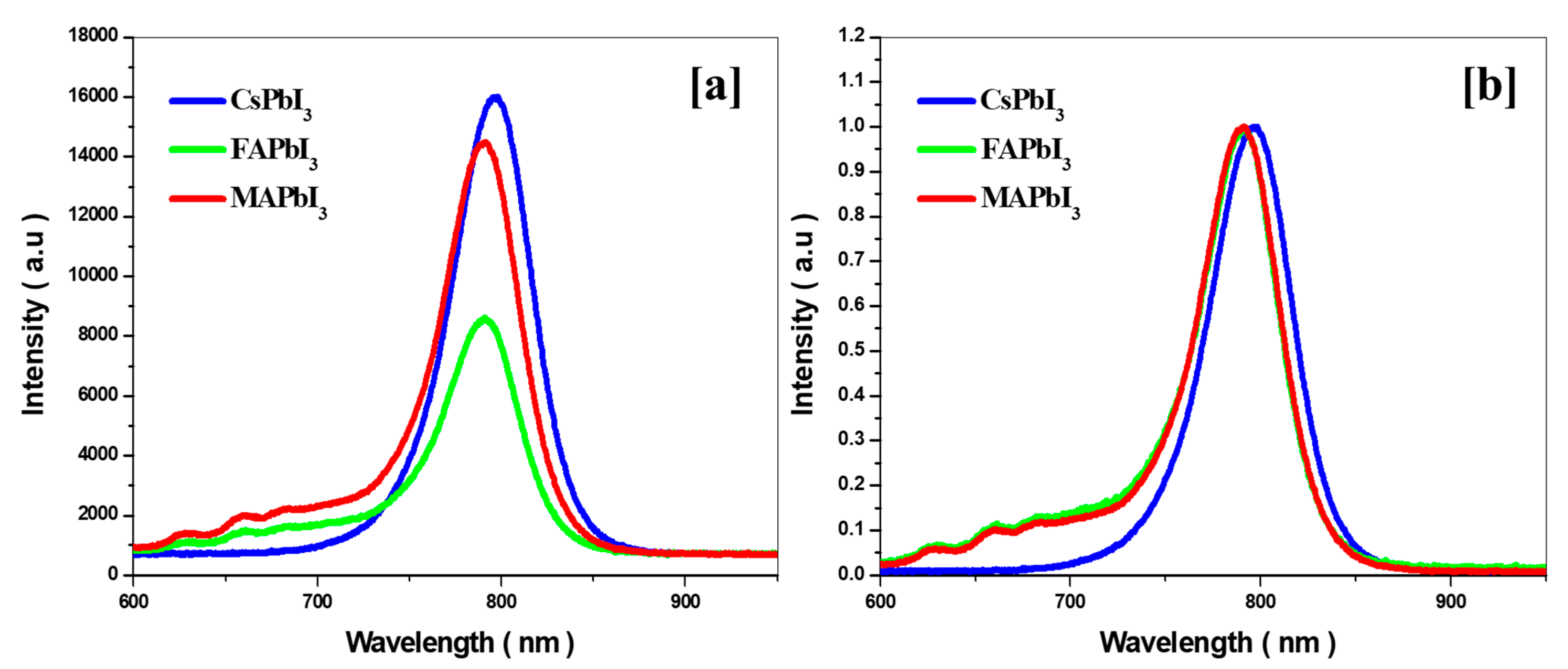
| Sample ID | Optical Band Gap by Absorption | Emission PL Peak | Stokes Shift | ||
|---|---|---|---|---|---|
| 719 | 1.55 | 760 | 1.40 | 150 | |
| 795 | 1.50 | 770 | 1.35 | 150 | |
| 752 | 1.53 | 768 | 1.36 | 180 | |
| Parameters | |||||
|---|---|---|---|---|---|
| 0.6 | 0.4 | 0.4 | 0.4 | 0.1 | |
| 3 | 1.55 | 1.5 | 1.53 | 3.2 | |
| 2.45 | 3.9 | 4.0 | 3.88 | 4 | |
| 3 | 10 | 6.6 | 6 | 9 | |
| 0.0002 | 11.8 | 2.7 | 16 | 20 | |
| 0.0002 | 11.8 | 2.8 | 16 | 10 |
| Defect Properties | |||
|---|---|---|---|
| 0.6 | 0.6 | 0.32 | |
| : Total density : Energy level : Holes and electrons capture cross section area | |||
| Samples | Fabricated Samples PCE [%] | Degraded Samples PCE [%] | Loss Percentage in PCE [%] |
|---|---|---|---|
| 22.93 | 18.29 | 20.24 | |
| 20.74 | 11.52 | 44.46 | |
| 19.12 | 16.39 | 14.28 |
| Samples | Degraded Samples PCE [%] | Recovered Samples PCE [%] | Gain Percentage in PCE [%] |
|---|---|---|---|
| 18.29 | 19.09 | 4.37 | |
| 11.52 | 12.04 | 4.51 | |
| 16.39 | 17.90 | 9.21 |
Publisher’s Note: MDPI stays neutral with regard to jurisdictional claims in published maps and institutional affiliations. |
© 2022 by the authors. Licensee MDPI, Basel, Switzerland. This article is an open access article distributed under the terms and conditions of the Creative Commons Attribution (CC BY) license (https://creativecommons.org/licenses/by/4.0/).
Share and Cite
Bouich, A.; Marí-Guaita, J.; Baig, F.; Hameed Khattak, Y.; Soucase, B.M.; Palacios, P. Investigation of the Surface Coating, Humidity Degradation, and Recovery of Perovskite Film Phase for Solar-Cell Applications. Nanomaterials 2022, 12, 3027. https://doi.org/10.3390/nano12173027
Bouich A, Marí-Guaita J, Baig F, Hameed Khattak Y, Soucase BM, Palacios P. Investigation of the Surface Coating, Humidity Degradation, and Recovery of Perovskite Film Phase for Solar-Cell Applications. Nanomaterials. 2022; 12(17):3027. https://doi.org/10.3390/nano12173027
Chicago/Turabian StyleBouich, Amal, Julia Marí-Guaita, Faisal Baig, Yousaf Hameed Khattak, Bernabé Marí Soucase, and Pablo Palacios. 2022. "Investigation of the Surface Coating, Humidity Degradation, and Recovery of Perovskite Film Phase for Solar-Cell Applications" Nanomaterials 12, no. 17: 3027. https://doi.org/10.3390/nano12173027
APA StyleBouich, A., Marí-Guaita, J., Baig, F., Hameed Khattak, Y., Soucase, B. M., & Palacios, P. (2022). Investigation of the Surface Coating, Humidity Degradation, and Recovery of Perovskite Film Phase for Solar-Cell Applications. Nanomaterials, 12(17), 3027. https://doi.org/10.3390/nano12173027