Abstract
In this study, we design ultra-broadband optical absorbers, ultra-narrow optical waveguides, and ultra-small optical cavities comprising two-dimensional metallic photonic crystals that tolerate fabrication imperfections such as position and radius disorderings. The absorbers containing gold rods show an absorption amplitude of more than 90% under 54% position disordering at nm. The absorbers containing silver rods show an absorptance of more than 90% under 54% position disordering at nm. B-type straight waveguides that contain four rows of silver rods exposed to air reveal normalized transmittances of 75% and 76% under 32% position and 60% radius disorderings, respectively. B-type L-shaped waveguides containing four rows of silver rods show 76% and 90% normalized transmittances under 32% position and 40% radius disorderings, respectively. B-type cavities containing two rings of silver rods reveal 70% and 80% normalized quality factors under 32% position and 60% radius disorderings, respectively.
1. Introduction
Metallic photonic crystals (MPHCs) have brought a new era for manipulating electromagnetic waves at the nanoscale. They are periodic metallic structures in which permittivity modulation occurs in one (grating) [1,2], two [3,4,5], and three dimensions [6,7,8]. These structures have the merits of low costs, easy fabrication, and small sizes, making them candidates for application in optical integrated circuits. The constitutive parts of the metallic structures are mainly gold (Au) and silver (Ag) that exhibit both negative and positive real permittivity, showing extraordinary responses to electromagnetic waves [9,10,11]. The materials have a high carrier concentration and low mobility; this entails a substantially negative real permittivity and material loss [12], which are accountable for reflectance and absorption, respectively. Due to the reflection, a metallic photonic bandgap (PBG), a frequency region that acts as a mirror to block electromagnetic waves, appears in MPHCs [7,13,14,15]. Several crucial optical components have been designed, such as filters [16,17], waveguides [18,19], and cavities [20,21], using PBGs. Based on the absorption in the metallic materials, several optical absorbers have been designed [22,23,24]. The metallic absorbers operating over ultra-violet (UV) and visible wavelengths are mainly applicable in photodetectors, control of thermal radiations, and photovoltaics. Owing to the reflection property of MPHCs, they are crucial candidates in designing waveguides and cavities. Waveguides are the key components in photonic devices that interconnect sources and detectors, called nanocircuits. They have proven their effectiveness over the visible spectrum in mode conversion [25], multimode polarization manipulation [26], coherent control of nanoscale directional couplers [27], and circuits for visible quantum emitters [28]. Optical cavities localize and enhance light beyond the diffraction limit and within a small volume. These components are vastly utilized in various nanolasers such as spasers [29,30], Fabry–Perot lasers [31,32], and whispering-gallery-resonator-based lasers [33,34].
Reducing the size of MPHCs for subwavelength operation (corresponding to the visible and UV spectra) brings a new challenge of fabrication imperfections [2,5,7,8,13,15,35] for optical components, such as absorbers, waveguides, and cavities. The imperfections appear as position and radius disorderings that influence the functionality of the structures [13,15,36,37,38]. As a result, designing ultra-broadband absorbers for UV and visible light, ultra-narrow and highly efficient waveguides for visible light, and ultra-small and high-quality-factor cavities for visible light that tolerate fabrication imperfections is of great importance.
This research theoretically studies the effects of fabrication imperfections on absorbers, waveguides, and cavities over the interval spectrum of nm. The optical components are designed using 2D MPHCs. The 2D MPHCs contain long Au or Ag cylinders in periodic arrangements of cubic and hexagonal patterns in air. Ultra-narrow waveguides and ultra-small cavities are designed using two rows of cylindrical Ag exposed to air, which tolerate fabrication imperfections.
The paper contains three sections. The second section describes two types of fabrication imperfections for the 2D MPHCs that elucidate the design procedure of absorbers with tolerance to fabrication imperfections; also it describes the design of straight and L-shaped waveguides and cavities under position and radius disorderings. The last part provides conclusions.
2. The Effects of Disorderings
In the subwavelength regime, the effect of fabrication imperfections is inevitable in 2D MPHCs. Fabrication imperfections are categorized as position and radius disorderings. By introducing and as the position of a rod, the position disordering parameter is introduced as , where is the origin position, is the strength of disordering, a is the lattice constant, and is a random variable over an interval [−1, 1] [36,37,38,39]. For the radius disordering, the radius of a rod is , where is the origin position of the rod, is the strength of the radius disordering, and is a random variable over the interval [−1, 1]. The radius-disordering parameter is [39]. The effect of disordering is used in designing ultra-broadband optical absorbers, ultra-narrow waveguides, and ultra-small cavities that tolerate position and radius disorderings to some extent. The 2D finite-difference time-domain (FDTD) module of Lumerical software is utilized to numerically calculate derived Maxwell’s equations on the 2D MPHC structures.
2.1. Ultra-Broadband Optical Absorbers
The structure of the 2D MPHC absorbers consists of an array of cylindrical metallic rods (either Au [40] or Ag [41]) exposed to air in a cubic pattern (Figure 1a,d). The radius and lattice constant of the structures are r = 15 nm and a = 130 nm, respectively. The 2D MPHCs under position disordering at and radius disordering at are shown in Figure 1a,d, respectively. Transverse electric (TE) polarized (electric field along the x-direction) plane waves are illuminated from the bottom and recorded from the top of the structures.
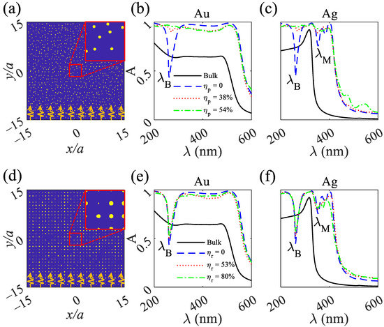
Figure 1.
(a) Schematic of 2D MPHC absorbers consist of cylindrical metallic rods in air at . (b,c) show absorption spectra for Au and Ag, respectively, under = 0, 38, and 54%. (d) Schematic of 2D MPHC absorbers consist of cylindrical metallic rods in air at . (e,f) show absorption spectra for Au and Ag, respectively, under = 0, 53, and 80%. The insets in (a,d) show the magnification of cylindrical rods in air. The yellow color shows the cylindrical rods, either Au or Ag, and the blue color shows air. TE polarized plane waves are depicted in an orange color and located at the bottom of (a,d) and they propagate from to y directions and recorded at the top of the structures. and stand for Bragg and Mie wavelengths, respectively.
The simulation result for a bulk Au reveals the absorption amplitude of 0.64 over a wavelength range of 280–480 nm, while the absorption amplitude sharply decreases at nm (Figure 1b,e); solid black line). The absorption for the bulk Au is due to the higher imaginary permittivity over the wavelength range, and the sharp decrease is due to lower imaginary permittivity and higher negative real permittivity (higher reflection) (Figure 2b). Shining a plane wave upon the 2D MPHCs containing Au cylinders exposed to air at (no position disordering) reveals an absorption of more than 0.95 over nm and a dip at nm, which shows the effect of periodicity and is called the Bragg bandgap. At , the input wave is reflected, and the intrinsic absorption limits the reflection amplitude owing to the imaginary permittivity. In contrast to the bulk gold, the 2D MPHC reveals higher and broadband absorption owing to the increased surface of the structure and enhanced interaction of light with matter. Increasing the position disordering of to , increases the bandwidth of absorption. The broad bandwidth absorption results from the disappearing of the Bragg dip. Bragg wavelength obeys , where is the propagation angle, which strongly depends on the lattice constant and the angle of propagation. Increasing the position disordering deteriorates a and ; as a result, the Bragg wavelength disappears (Figure 1b,c). Although increasing the position disordering increases the absorption bandwidth, increasing the radius disordering does not change the periodicity; as a result, the Bragg wavelength and the absorption bandwidth remain unaffected (Figure 1e,f).
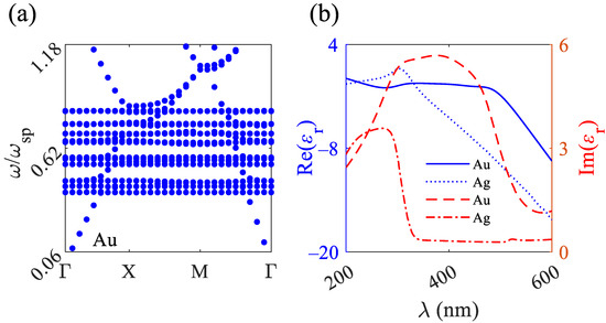
Figure 2.
(a) Band structure of 2D MPHCs consists of Au rods in air under TE polarized light. (b) The real and imaginary parts of permittivity for Au and Ag over a wavelength range of 200–600 nm.
Bulk silver under the TE polarized plane wave illumination reveals an absorption of approximately 0.73 over nm that is due to the higher imaginary permittivity (Figure 2b; dot-dashed red curve). An absorption peak of 0.9 at nm is due to the positive real permittivity peak at the wavelength, which suppresses the reflection (Figure 2b; dotted blue curve). At nm, the absorption decreases sharply, owing to the lower imaginary permittivity and higher negative real permittivity, that results in increasing the reflection. Illuminating the plane wave upon the 2D MPHC containing Ag components at (no radius and position disorderings) reveals absorption spectra with two dips. The first dip at nm is a Bragg wavelength that shows the reflection, and the other occurs at nm owing to Mie scattering. By increasing the position disordering from to , the Bragg and Mie dips disappear, resulting in a broad bandwidth with an absorption amplitude . In contrast to the position disordering, by increasing the radius disordering from to , the absorption spectra remain unchanged due to the preserving of lattice constant and propagation angle. Owing to the low negative real and positive imaginary permittivity (Figure 2b; solid blue and dashed red curves), the Mie wavelength shows a weak dip and is mainly affected by position disordering (Figure 1b,c).
The photonic band structure explains the absorbance for the 2D MPHCs. In this study, as an example, the band structure of a 2D MPHC containing Au rods exposed to air under exposure to TE polarized waves is calculated. The imaginary permittivity of the metallic rods causes fast decaying in electromagnetic fields and an inaccurate band structure; as a result, for calculation of the band structure, the imaginary permittivity of Au is considered to be zero. The band structure contains numerous flat bands over high absorption spectra approximating the surface-plasmon frequency (Figure 2a). for Au is [42]. The flat bands reveal a slow-light regime that results in the high coupling of light to the MPHCs. The physics behind the absorption of the 2D MPHC absorbers originate from impedance matching between the structure and air. For the structure, the effective permittivity and permeability are defined as and , respectively, as a result, the effective refractive index of the structure is . The impedance matching between the structure and air happens when the refractive index of the structure is approximately the same as the refractive index of air (). Under the impedance matching condition, , that reveals the perfect absorption [43,44].
The electrical field distributions of the absorbers containing either Au or Ag cylindrical rods under at reveal the penetration of electromagnetic waves into the structure, resulting in high absorption of the waves (Figure 3a,b); the electrical field distributions of the structure under represent the penetration of electromagnetic waves into the structure, indicating the absorption of the waves, which is due to the loss of the metallic rods and also the distributions reveal the reflection of the waves owing to the periodicity of the structure (Figure 3c,d). The comparisons between the previous studies and the proposed absorber are represented in Table 1. Although References [45,46,47] show high average absorption, they do not cover the ultra-violet spectrum. Additionally, their high average absorption is due to the high extinction coefficient of Tungsten. Ref. [48] covers the ultra-violet spectrum, but it suffers from low average absorption. Our structure reveals the highest average absorption that also covers the ultra-violet spectrum. The other merit of our proposed absorber is immune to fabrication disorderings; as a result, it shows the lack of dependency on the angle of incident light.
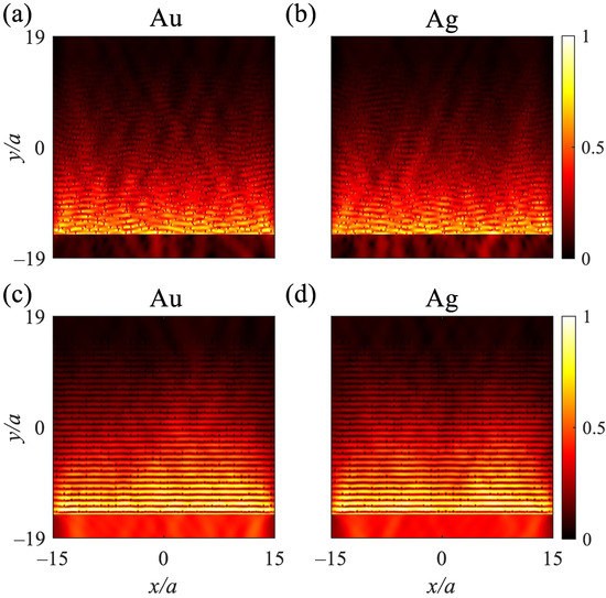
Figure 3.
Normalized electrical field distribution of the absorber containing cylindrical (a) Au and (b) Ag rods in air under , respectively. Normalized electrical field distribution of the absorber under containing cylindrical (c) Au and (d) Ag rods in air, respectively. The electrical field distribution are recorded at ; TE polarized plane waves are located at the bottom of the structure and propagate from to y directions and recorded at the top of the structures.

Table 1.
The comparison of the present work and some recent works.
2.2. Designing Optical Waveguides and Cavities
Here, 2D MPHC waveguides consisting of Ag rods exposed to air under transverse magnetic (TM) polarized light illumination are designed. The structural parameters are r = 50 nm and a = 160 nm. Ag has a lower and constant imaginary permittivity and higher negative real permittivity over nm, which results in low absorption and high reflection (Figure 2). The reflection region reveals a metallic band gap, which can be explained by the bond theory. The Bond theory for 2D MPHCs assumes an optical state in the form of a quasi-bond state for each rod. The quasi-bond state for each rod couples to its adjacent rod and create a PBG between quasi-bond states [15]. Owing to the high skin depth of Ag and Au at nm, each rod exhibits optical states, and the bond theory is applicable in the case of the 2D MPHCs (Figure S1).
Electrical field distributions show electric hotspots between the rods along the x-direction under a TE polarized plane wave (Figure S2a) and no electric hotspots under the illumination of a TM polarized plane wave (Figure S2b). Under TE circumstances, the incident wave causes the creation of electric dipoles (P) in each rod and results in coupling between them. Under TM conditions, the electric dipoles do not couple, and the hotspots do not appear between the Ag rods. Under the TM polarized incident light wave, the 2D MPHC structure behaves as a mirror that blocks electromagnetic waves and is called a metallic bandgap that is suitable for designing optical components.
The absorption and reflection spectra of the 2D MPHCs containing Ag rods exposed to air show robustness to the position disordering at and the radius disordering at (Figure 4). Owing to the high imaginary permittivity, the absorption is high at nm, and owing to the low imaginary permittivity and high negative real permittivity, absorption is less, and reflection is high at nm. The first reason behind the robustness of the absorption and reflection spectra to high position and radius disorderings is the high imaginary permittivity and high negative real permittivity of Ag, respectively (Figure 2b). The second reason is the creation of quasi-bond states due to the penetration of electromagnetic waves in Ag (skin depth) and the coupling of the quasi-bond states that causes a robust bandgap under disordering. Owing to the structural parameters and the TM polarized incident plane wave, none of the Bragg and Mie dips appear in the absorption and reflection spectra (Figure 4). Furthermore, in the incident TM polarized wave (electric field is along the long axis of rods), the surface plasmons are not excited. By exploiting the robustness of the reflection to the position and radius disorderings over nm, the straight and L-shaped waveguides and cavities are designed.
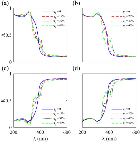
Figure 4.
Absorption (A) spectra for 2D MPHCs consist of Ag rods in air under TM polarized illuminations under (a) position and (b) radius disorderings. Reflection (R) spectra of the 2D MPHCs consisting Ag rods in air under TM polarized illuminations under (c) position and (d) radius disorderings.
2.2.1. Ultra-Narrow Straight and L-Shaped Optical Waveguides
Three types of straight and L-shaped waveguides are designed using the 2D MPHCs containing Ag rods exposed to air. Creating straight or L-shaped defects in the structure localizes a guided mode inside the reflection spectra nm (Figure S3). The guided modes propagate inside the defects with high transmission efficiency. The straight (Figure 5a,d) and L-shaped (Figure 5g,j) defects inside the structure are called A-type structures. The straight (Figure 5b,e) and L-shaped (Figure 5h,k) waveguides with four rows of Ag rods exposed to air are called B-type structures. The straight (Figure 5c,f) and L-shaped (Figure 5i,l) waveguides with two rows of Ag rods exposed to air are called C-type structures. The incident waves are TM polarized Gaussian in orange, illuminated at the bottom of the waveguides, which are propagated from to y and recorded at the top for the straight and the right for the L-shaped waveguides, respectively (Figure 5).
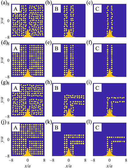
Figure 5.
2D MPHCwaveguides contain Ag rods in air. (a–f) show straight waveguides of A, B, and C at and , respectively. (g–l) show A, B, and C-type L-shaped waveguides at and , respectively. At the bottom of the waveguides, the orange bell shapes are Gaussian waves that propagate from −y to y and are recorded at the top and right of the straight and L-shaped waveguides, respectively—yellow: Ag rods and blue: air.
The normalized transmission amplitudes () of the straight waveguides are high and approximately the same for A and B with at and at , respectively. Additionally, they reveal at and at ((Figure 6a,e); solid black and dashed blue curves, respectively). The normalized transmission amplitudes under the radius disordering for the A and B structures are higher than those under the position disordering. Higher normalized transmission amplitudes are due to the preserving periodicity of the structure. The normalized transmissions for C-type straight waveguides are lower than A and B, originating from fewer rods. Owning to the large distances created between adjacent rods by the breaking symmetry of the position disordering, the normalized transmission amplitude is less than that in the case with radius disordering (Figure 6a,e). As noticeable from the logarithmic electromagnetic power distributions at nm, the A and B-type straight waveguides at show high-confinement of electromagnetic waves (Figure 6b,c) and escaping electromagnetic waves for the C-type waveguide (Figure 6d). Additionally, the A and B-type waveguides at shows high confinement of light due to the preserved periodicity of the structure (Figure 6f,g); the C-type structure at shows the escape of electromagnetic waves to air (Figure 6h).
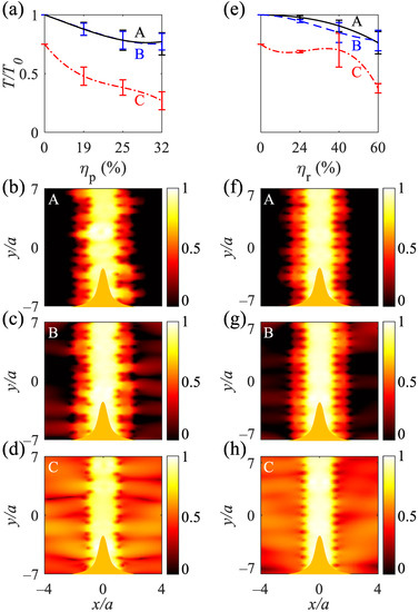
Figure 6.
Normalized transmission for the straight A-, B-, and C-type waveguides under the (a) position disordering at = 19, 25, and 32% and (e) radius disordering at = 24, 40, and 60%. (b–d) Normalized logarithmic electromagnetic power distributions at nm for A, B, and C-type waveguides under . (f–h) Normalized logarithmic electromagnetic power distributions at nm for A, B, and C-type waveguides under . The orange bell shapes at the bottom of (b–d,f–h) show the TM polarized Gaussian waves, propagating from to y, and are recorded at the top of the waveguides.
The normalized transmission amplitudes for the L-shaped waveguides are high enough and approximately the same for A- and B-type waveguides under position and radius disorderings ((Figure 7a,e); solid black and dashed blue curves, respectively). The A and B types tolerate the position disordering at with , and the waveguides tolerate the radius disordering at with . As evident, reducing the number of rows from 14 (A-type) to 4 (B-type) does not change the normalized transmission amplitude under the position and radius disorderings at and . decreases at higher position and radius disorderings owing to the greater distances between the rods (Figure 7a,e). for C-type L-shaped waveguide at and for the waveguide at . The logarithmic electromagnetic power distributions for the A- and B-type L-shaped waveguides at nm and under either (Figure 7b,c) or (Figure 7f,g) reveal that a sharp bend does not change the guided mode to radiation modes, and the electromagnetic mode is preserved as a guided mode. Increasing the distance between the rods due to either the position or radius disorderings decreases the quasi-bond modes coupling between the rods and reduces the transmission amplitudes and results in fleeing electromagnetic waves (Figure 7d,h). The average transmissions of straight and L-shaped waveguides versus position and radius disorderings are summerized in Table 2 and Table 3, respectively. Owing to the imaginary permittivity of silver over the metallic band, increasing the length of the straight and L-shaped waveguides exponentially decreases the normalized transmittance. For the B-type straight and L-shaped waveguides, the normalized transmittance follows the exponential functions of and , respectively (where N = 1, 2, ⋯ is the number of removed silver rods).
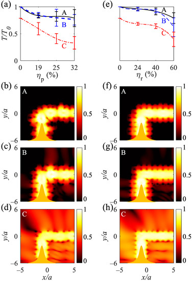
Figure 7.
Normalized transmission for the A-, B-, and C-type L-shaped waveguides under the (a) position disordering under = 19, 25, and 32% and (e) radius disordering under = 24, 40, and 60%. (b–d) Normalized logarithmic electromagnetic power distributions at nm for A, B, and C-type L-shaped waveguides under . (f–h) Normalized logarithmic electromagnetic power distributions at nm for A, B, and C-type L-shaped waveguides under . The orange bell shapes at the bottom of (b–d,f–h) show the TM polarized Gaussian waves, propagating from to y, and are recorded at the right of the waveguides.

Table 2.
The average normalized transmission for the straight waveguide under radius and position disorderings.

Table 3.
The average normalized transmission for the L-shaped waveguide under radius and position disorderings.
2.2.2. Ultra-Small Cavities
In this part, the cavities are created by removing a rod (point defect) from the 2D MPHCs that contain Ag rods in a hexagonal pattern. Making a point defect, localizes a high-quality mode over the metallic bandgap () and is used to design the cavities (Figure S4). Three cavities are introduced regarding the number of surrounded Ag rods as a ring from the point defect. A point defect surrounded by eight, two, and one rings of Ag rods are called A- (Figure 8a,d), B- (Figure 8b,e), and C- (Figure 8c,f) type cavities, respectively. The TM polarized dipole sources are placed in the defect area where the light is recorded using point monitors.
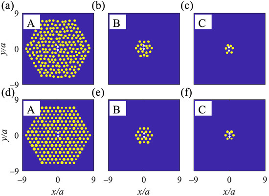
Figure 8.
2D MPHC structure under contains Ag rods in air with a removed rod at the center surrounded by (a) eight, (b) two, and (c) one rings of Ag rods. The structure under containing Ag rods in air with a removed rod at the center surrounded by (d) eight, (e) two, and (f) one rings of Ag rods. Yellow: Ag rods and blue: air. White-double arrows at the center of each cavity show TM polarized dipole sources.
The average normalized quality factor () for the A-type cavities is more than 1 at the position disordering , indicating an increase in the constructive interference of light due to the interaction of light by several rings of Ag rods (Figure 9a; solid black curve). Additionally, the quality factor variance increases with increasing the position disordering owing to the escaping electromagnetic waves between the rods. The B-type cavities has higher variations of the normalized quality factor under the position disordering due to the escaping electromagnetic waves over two rings of Ag rods. For the A-type cavities, at the radius disordering , and for B-type cavities at (Figure 9e). The A- and B-type cavities show lower variations under the radius disordering owing to the preservation of the periodicity of the structure. The C-type cavities show approximately the least constant normalized quality factor under the position and radius disorderings (Figure 9a,e; dot-dashed red curves). Moreover, the C-type cavities containing one ring of Ag rods cannot realize the high confinement of the light wave in the defect due to large distances between the rods. The normalized transmissions versus position and radius disorderings for the 2D MPHC cavities are summarized in Table 4. The logarithmic electromagnetic power distributions for the A- and B-type cavities at and 400 nm under (Figure 9b,c) and at and 410 nm under (Figure 9f,g) reveal the high confinement of the electromagnetic waves. Additionally, the C-type cavities at nm under (Figure 9d) and at nm under (Figure 9h) show the confinement of the electromagnetic waves at the center and escaping of electromagnetic waves owning to the large distances between rods. Owing to the high negative real permittivity of the Ag rods, the position and radius disorderings apply a phase difference, resulting in variations in the frequency of the guided mode under the straight and L-shaped defects and confined modes in the cavities.
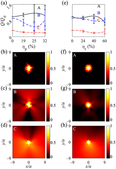
Figure 9.
Normalized quality factor for A-, B-, and C-type cavities under (a) = 19, 25, and 32% and (e) = 24, 40, and 60%. (b–d) Normalized logarithmic electromagnetic power distributions for the A, B, and C-type cavities at , and 400 nm, respectively. (f–h) Normalized logarithmic electromagnetic power distributions for the A, B, and C-type cavities at , and 410 nm, respectively.

Table 4.
The average normalized quality factor for the cavity under radius and position disorderings.
3. Conclusions
This paper theoretically proposed three optical components, namely absorbers, waveguides, and cavities. The components contain 2D metallic (Au and Ag for absorbers and Ag for waveguides and cavities) rods exposed to air. The absorbers consist of 2D MPHC of gold rods in air represented under over the nm. The 2D FDTD simulation results for the A-type straight waveguides showed and 0.78 under and , respectively, also, for A-type L-shaped waveguides and 0.79 under and , respectively. The simulation results for the B-type straight waveguides revealed and 0.85 under and , respectively. The results for the B-type L-shaped waveguides represented and 0.92 under and , respectively. The B-type cavities reveal and 0.8 under and , respectively. The designed ultra-broadband absorbers are potential components for achieving photodetectors, thermal radiation control, and photovoltaics. The ultra-narrow waveguides are crucial components for nanocircuits in polarization manipulation, control coherent, quantum emitters, and color routers for complementary metal-oxide-semiconductor image sensors. The ultra-small cavities are potential candidates for application in high-density integrated circuits and nanolasers.
Supplementary Materials
The following supporting information can be downloaded at: https://www.mdpi.com/article/10.3390/nano12132132/s1. Figure S1: Skin depth for gold and silver over a wavelength range of 0.2–0.6 mm; Figure S2: Normalized electrical field distribution over the structure under (a) TE and (b) TM polarized incident plane waves with no position and radius disorderings; Figure S3: Transmission for 2D MPHCs consists of 15 × 15 silver rods in air under TM polarized Gaussian wave for the A, B, and C types of (a) straight and (b) L-shaped waveguides. For calculating the transmission spectra, no position and radius disorderings are considered; Figure S4: Normalized electric field spectra of 2D MPHCs contain silver rods in air for A, B, and C cavities.
Author Contributions
Conceptualization, K.G. and M.L.; methodology, K.G.; software, K.G.; validation, K.G. and M.L.; formal analysis, M.L.; investigation, K.G. and M.L.; resources, M.L.; data curation, K.G. and M.L.; writing—original draft preparation, K.G.; writing—review and editing, K.G. and M.L.; visualization, K.G. and M.L.; supervision, M.L.; project administration, M.L.; funding acquisition, M.L. All authors have read and agreed to the published version of the manuscript.
Funding
We wish to acknowledge the financial support from the BK21 FOUR program and Educational Institute for Intelligent Information Integration, Samsung Electronics Co., Ltd. (IO201211-08121-01), and Samsung Science and Technology Foundation (SRFC-TC2103-01).
Data Availability Statement
The data presented in this study are available in this article and its supplementary material.
Conflicts of Interest
The authors declare no conflict of interest.
References
- Li, D.; Ou, J.Y.; Xie, P.; Liang, Z.; Wang, W.; Wang, W.; Zhang, H.; Kuang, X. Spectroscopic study of gap-surface plasmons in a metallic convex groove array and their applications in nanofocusing and plasmonic sensing. Phys. Rev. B 2021, 103, 245404. [Google Scholar] [CrossRef]
- Sarkar, S.; Gupta, V.; Tsuda, T.; Gour, J.; Singh, A.; Aftenieva, O.; Steiner, A.M.; Hoffmann, M.; Kumar, S.; Fery, A.; et al. Plasmonic charge transfers in large-scale metallic and colloidal photonic crystal slabs. Adv. Funct. Mater. 2021, 31, 2011099. [Google Scholar] [CrossRef]
- Sugavaneshwar, R.P.; Ishii, S.; Dao, T.D.; Ohi, A.; Nabatame, T.; Nagao, T. Fabrication of highly metallic TiN films by pulsed laser deposition method for plasmonic applications. ACS Photonics 2017, 5, 814–819. [Google Scholar] [CrossRef]
- Honari-Latifpour, M.; Yousefi, L. Topological plasmonic edge states in a planar array of metallic nanoparticles. Nanophotonics 2019, 8, 799–806. [Google Scholar] [CrossRef]
- Garoli, D.; Mosconi, D.; Miele, E.; Maccaferri, N.; Ardini, M.; Giovannini, G.; Dipalo, M.; Agnoli, S.; De Angelis, F. Hybrid plasmonic nanostructures based on controlled integration of MoS2 flakes on metallic nanoholes. Nanoscale 2018, 10, 17105–17111. [Google Scholar] [CrossRef] [PubMed] [Green Version]
- El-Kady, I.; Sigalas, M.; Biswas, R.; Ho, K.; Soukoulis, C. Metallic photonic crystals at optical wavelengths. Phys. Rev. B 2000, 62, 15299. [Google Scholar] [CrossRef] [Green Version]
- Fleming, J.; Lin, S.; El-Kady, I.; Biswas, R.; Ho, K. All-metallic three-dimensional photonic crystals with a large infrared bandgap. Nature 2002, 417, 52–55. [Google Scholar] [CrossRef]
- Vasilantonakis, N.; Terzaki, K.; Sakellari, I.; Purlys, V.; Gray, D.; Soukoulis, C.M.; Vamvakaki, M.; Kafesaki, M.; Farsari, M. Three-dimensional metallic photonic crystals with optical bandgaps. Adv. Mater. 2012, 24, 1101–1105. [Google Scholar] [CrossRef]
- Frank, B.; Kahl, P.; Podbiel, D.; Spektor, G.; Orenstein, M.; Fu, L.; Weiss, T.; Horn-von Hoegen, M.; Davis, T.J.; Zu Heringdorf, F.J.M.; et al. Short-range surface plasmonics: Localized electron emission dynamics from a 60-nm spot on an atomically flat single-crystalline gold surface. Sci. Adv. 2017, 3, e1700721. [Google Scholar] [CrossRef] [Green Version]
- Wu, Y.; Hu, Z.; Kong, X.T.; Idrobo, J.C.; Nixon, A.G.; Rack, P.D.; Masiello, D.J.; Camden, J.P. Infrared plasmonics: STEM-EELS characterization of Fabry-Perot resonance damping in gold nanowires. Phys. Rev. B 2020, 101, 085409. [Google Scholar] [CrossRef]
- Karst, J.; Floess, M.; Ubl, M.; Dingler, C.; Malacrida, C.; Steinle, T.; Ludwigs, S.; Hentschel, M.; Giessen, H. Electrically switchable metallic polymer nanoantennas. Science 2021, 374, 612–616. [Google Scholar] [CrossRef] [PubMed]
- Boltasseva, A.; Atwater, H.A. Low-loss plasmonic metamaterials. Science 2011, 331, 290–291. [Google Scholar] [CrossRef]
- Ma, J.; Ouyang, C.; Niu, L.; Wang, Q.; Zhao, J.; Liu, Y.; Liu, L.; Xu, Q.; Li, Y.; Gu, J.; et al. Topological edge state bandwidth tuned by multiple parameters in two-dimensional terahertz photonic crystals with metallic cross structures. Opt. Express 2021, 29, 32105–32113. [Google Scholar] [CrossRef] [PubMed]
- Wang, Y.; Zhou, X.; Li, S.; Zhang, W.; Hu, C.; Lu, W.; Hou, B. Flatness and boundness of photonic drumhead surface state in a metallic lattice. Sci. Rep. 2021, 11, 1–7. [Google Scholar] [CrossRef]
- Jiang, H.; Liu, W.; Xu, J.; Gao, B.; Zhu, C.; Xie, S.; Yang, Y. Topological edge modes in one-dimensional photonic crystals containing metal. OSA Contin. 2021, 4, 1626–1639. [Google Scholar] [CrossRef]
- Chau, Y.F.C.; Chao, C.T.C.; Chiang, H.P. Ultra-broad bandgap metal-insulator-metal waveguide filter with symmetrical stubs and defects. Results Phys. 2020, 17, 103116. [Google Scholar] [CrossRef]
- Jang, J.; Kang, K.; Raeis-Hosseini, N.; Ismukhanova, A.; Jeong, H.; Jung, C.; Kim, B.; Lee, J.Y.; Park, I.; Rho, J. Self-powered humidity sensor using chitosan-based plasmonic metal-hydrogel-metal filters. Adv. Opt. Mater. 2020, 8, 1901932. [Google Scholar] [CrossRef]
- Zheng, K.; Song, J.; Qu, J. Hybrid low-permittivity slot-rib plasmonic waveguide based on monolayer two dimensional transition metal dichalcogenide with ultra-high energy confinement. Opt. Express 2018, 26, 15819–15824. [Google Scholar] [CrossRef]
- Gosciniak, J.; Atar, F.B.; Corbett, B.; Rasras, M. Plasmonic Schottky photodetector with metal stripe embedded into semiconductor and with a CMOS-compatible titanium nitride. Sci. Rep. 2019, 9, 1–12. [Google Scholar] [CrossRef] [Green Version]
- Hugall, J.T.; Singh, A.; van Hulst, N.F. Plasmonic cavity coupling. ACS Photonics 2018, 5, 43–53. [Google Scholar] [CrossRef]
- Kwon, J.A.; Jin, C.M.; Shin, Y.; Kim, H.Y.; Kim, Y.; Kang, T.; Choi, I. Tunable plasmonic cavity for label-free detection of small molecules. ACS Appl. Mater. Interfaces 2018, 10, 13226–13235. [Google Scholar] [CrossRef] [PubMed]
- Chaudhuri, K.; Alhabeb, M.; Wang, Z.; Shalaev, V.M.; Gogotsi, Y.; Boltasseva, A. Highly broadband absorber using plasmonic titanium carbide (MXene). Acs Photonics 2018, 5, 1115–1122. [Google Scholar] [CrossRef]
- Lei, L.; Li, S.; Huang, H.; Tao, K.; Xu, P. Ultra-broadband absorber from visible to near-infrared using plasmonic metamaterial. Opt. Express 2018, 26, 5686–5693. [Google Scholar] [CrossRef] [PubMed]
- Bonin, G.O.; Barrow, S.J.; Connell, T.U.; Roberts, A.; Chesman, A.S.; Gomez, D.E. Self-assembly of plasmonic near-perfect absorbers of light: The effect of particle size. J. Phys. Chem. Lett. 2020, 11, 8378–8385. [Google Scholar] [CrossRef]
- Dai, W.H.; Lin, F.C.; Huang, C.B.; Huang, J.S. Mode conversion in high-definition plasmonic optical nanocircuits. Nano Lett. 2014, 14, 3881–3886. [Google Scholar] [CrossRef]
- Gan, F.; Sun, C.; Wang, Y.; Li, H.; Gong, Q.; Chen, J. Multimode metallic double-strip waveguides for polarization manipulation. Adv. Mater. Technol. 2017, 2, 1600248. [Google Scholar] [CrossRef]
- Rewitz, C.; Razinskas, G.; Geisler, P.; Krauss, E.; Goetz, S.; Pawlowska, M.; Hecht, B.; Brixner, T. Coherent control of plasmon propagation in a nanocircuit. Phys. Rev. Appl. 2014, 1, 014007. [Google Scholar] [CrossRef] [Green Version]
- Schorner, C.; Adhikari, S.; Lippitz, M. A single-crystalline silver plasmonic circuit for visible quantum emitters. Nano Lett. 2019, 19, 3238–3243. [Google Scholar] [CrossRef] [Green Version]
- Noginov, M.; Zhu, G.; Belgrave, A.; Bakker, R.; Shalaev, V.; Narimanov, E.; Stout, S.; Herz, E.; Suteewong, T.; Wiesner, U. Demonstration of a spaser-based nanolaser. Nature 2009, 460, 1110–1112. [Google Scholar] [CrossRef]
- Aellen, M.; Rossinelli, A.A.; Keitel, R.C.; Brechbuhler, R.; Antolinez, F.V.; Rodrigo, S.G.; Cui, J.; Norris, D.J. Role of gain in Fabry–Pérot surface plasmon polariton lasers. ACS Photonics 2022, 9, 630–640. [Google Scholar] [CrossRef]
- Xu, W.H.; Chou, Y.H.; Yang, Z.Y.; Liu, Y.Y.; Yu, M.W.; Huang, C.H.; Chang, C.T.; Huang, C.Y.; Lu, T.C.; Lin, T.R.; et al. Tamm plasmon-polariton ultraviolet lasers. Adv. Photonics Res. 2022, 3, 2100120. [Google Scholar] [CrossRef]
- Duan, R.; Zhang, Z.; Xiao, L.; Zhao, X.; Thung, Y.T.; Ding, L.; Liu, Z.; Yang, J.; Ta, V.D.; Sun, H. Ultralow-threshold and high-quality whispering-gallery-mode lasing from colloidal core/hybrid-shell quantum wells. Adv. Mater. 2022, 34, 2108884. [Google Scholar] [CrossRef] [PubMed]
- Guo, Q.; Zhang, J.; Ning, C.; Zhuo, N.; Zhai, S.; Liu, J.; Wang, L.; Liu, S.; Jia, Z.; Liu, F. Continuous-wave operation of microcavity quantum cascade lasers in whispering-gallery mode. ACS Photonics 2022, 9, 1172–1179. [Google Scholar] [CrossRef]
- Price, M.B.; Lewellen, K.; Hardy, J.; Lockwood, S.M.; Zemke-Smith, C.; Wagner, I.; Gao, M.; Grand, J.; Chen, K.; Hodgkiss, J.M.; et al. Whispering-gallery mode lasing in perovskite nanocrystals chemically bound to silicon dioxide microspheres. J. Phys. Chem. Lett. 2020, 11, 7009–7014. [Google Scholar] [CrossRef] [PubMed]
- Yu, X.; Lee, Y.J.; Furstenberg, R.; White, J.O.; Braun, P.V. Filling fraction dependent properties of inverse opal metallic photonic crystals. Adv. Mater. 2007, 19, 1689–1692. [Google Scholar] [CrossRef]
- Goudarzi, K.; Lee, M. Super strong wide TM Mie bandgaps tolerating disorders. Sci. Rep. 2022, 12, 1–12. [Google Scholar] [CrossRef]
- Goudarzi, K.; Lee, M. Inverse design of a binary waveguide crossing by the particle swarm optimization algorithm. Results Phys. 2022, 34, 105268. [Google Scholar] [CrossRef]
- Goudarzi, K. Ultra-narrow, highly efficient power splitters and waveguides that exploit the TE01 Mie-resonant bandgap. Opt. Express 2021, 29, 32951–32965. [Google Scholar] [CrossRef]
- Liu, C.; Rybin, M.V.; Mao, P.; Zhang, S.; Kivshar, Y. Disorder-immune photonics based on Mie-resonant dielectric metamaterials. Phys. Rev. Lett. 2019, 123, 163901. [Google Scholar] [CrossRef] [Green Version]
- Babar, S.; Weaver, J. Optical constants of Cu, Ag, and Au revisited. Appl. Opt. 2015, 54, 477–481. [Google Scholar] [CrossRef]
- Johnson, P.B.; Christy, R.W. Optical constants of the noble metals. Phys. Rev. B 1972, 6, 4370. [Google Scholar] [CrossRef]
- Derkachova, A.; Kolwas, K.; Demchenko, I. Dielectric function for gold in plasmonics applications: Size dependence of plasmon resonance frequencies and damping rates for nanospheres. Plasmonics 2016, 11, 941–951. [Google Scholar] [CrossRef] [PubMed] [Green Version]
- Butt, M.; Khonina, S.; Kazanskiy, N.; Piramidowicz, R. Hybrid metasurface perfect absorbers for temperature and biosensing applications. Opt. Mater. 2022, 123, 111906. [Google Scholar] [CrossRef]
- Tao, H.; Landy, N.I.; Bingham, C.M.; Zhang, X.; Averitt, R.D.; Padilla, W.J. A metamaterial absorber for the terahertz regime: Design, fabrication and characterization. Opt. Express 2008, 16, 7181–7188. [Google Scholar] [CrossRef]
- Charola, S.; Patel, S.K.; Dalsaniya, K.; Jadeja, R.; Nguyen, T.K.; Dhasarathan, V. Numerical investigation of wideband L-shaped metasurface based solar absorber for visible and ultraviolet region. Phys. B Condens. Matter 2021, 601, 412503. [Google Scholar] [CrossRef]
- Hakim, M.L.; Alam, T.; Islam, M.S.; Salaheldeen M, M.; Almalki, S.H.; Baharuddin, M.H.; Alsaif, H.; Islam, M.T. Wide-oblique-incident-angle stable polarization-insensitive ultra-wideband metamaterial perfect absorber for visible optical wavelength applications. Materials 2022, 15, 2201. [Google Scholar] [CrossRef]
- Musa, A.; Hakim, M.L.; Alam, T.; Islam, M.T.; Alshammari, A.S.; Mat, K.; Almalki, S.H.; Islam, M.S. Polarization independent metamaterial absorber with anti-reflection coating nanoarchitectonics for visible and infrared window applications. Materials 2022, 15, 3733. [Google Scholar] [CrossRef]
- Ran, Y.; Jiang, Z.; Wang, Z. All-nitride broadband metamaterial absorbers. Results Phys. 2022, 38, 105657. [Google Scholar] [CrossRef]
- Mahmud, S.; Karim, M.; Islam, S.S.; Shuvo, M.M.K.; Akter, T.; Almutairi, A.F.; Islam, M.T. A multi-band near perfect polarization and angular insensitive metamaterial absorber with a simple octagonal resonator for visible wavelength. IEEE Access 2021, 9, 117746–117760. [Google Scholar] [CrossRef]
- Roostaei, N.; Mbarak, H.; Monfared, S.A.; Hamidi, S. Plasmonic wideband and tunable absorber based on semi etalon nano structure in the visible region. Phys. Scr. 2021, 96, 035805. [Google Scholar] [CrossRef]
Publisher’s Note: MDPI stays neutral with regard to jurisdictional claims in published maps and institutional affiliations. |
© 2022 by the authors. Licensee MDPI, Basel, Switzerland. This article is an open access article distributed under the terms and conditions of the Creative Commons Attribution (CC BY) license (https://creativecommons.org/licenses/by/4.0/).