Article

Thermal Conductivity of VO2 Nanowires at Metal-Insulator Transition Temperature

Center for Phononics and Thermal Energy Science, China-EU Joint Center for Nanophononics, School of Physics Science and Engineering, Tongji University, Shanghai 200092, China
*
Author to whom correspondence should be addressed.
Nanomaterials 2021, 11(9), 2428; https://doi.org/10.3390/nano11092428
Submission received: 16 August 2021 / Revised: 15 September 2021 / Accepted: 16 September 2021 / Published: 17 September 2021
(This article belongs to the Special Issue Heat Transfer in Nanostructured Materials)

Abstract

:
Vanadium dioxide (VO2) nanowires endowed with a dramatic metal−insulator transition have attracted enormous attention. Here, the thermal conductance of VO2 nanowires with different sizes, measured using the thermal bridge method, is reported. A size-dependent thermal conductivity was observed where the thicker nanowire showed a higher thermal conductivity. Meanwhile, the thermal conductivity jump at metal−insulator transition temperature was measured to be much higher in the thicker samples. The dominant heat carriers were phonons both at the metallic and the insulating regimes in the measured samples, which may result from the coexistence of metal and insulator phases at high temperature. Our results provide a window into exploring the mechanism of the metal−insulator transition of VO2 nanowires.

1. Introduction

Metal-insulator transition (MIT) has long been a widely researched centerpiece in condensed matter physics, with a number of efforts focusing on potentially exploiting the resulting changes in the functional properties in novel electronics and phononics, as well as understanding the emergent phenomena. In the 1950s, Morin first noted that the electrical resistance in some transition metal oxides increases by several orders of magnitude when the temperature crosses the transition temperature [1]. In recent years, vanadium oxide compounds, as a kind of typical strongly correlated electron materials, have attracted considerable interest for MIT. Among them, VO2, whose phase transition temperature is close to room temperature, has great potential applications in Mott field-effect transistors [2,3], optical temperature sensors [4], ultrafast photoelectric switch materials [5] and thermochromic devices [6], resulting in tremendous studies and hot research topics ongoing.
VO2 undergoes a first-order MIT at around 68 °C from a high-temperature metallic (M) phase to a low-temperature insulating (I) phase. Accompanying the electronic transition is a structural phase transition from a high-temperature tetragonal structure to a low-temperature monoclinic structure, making the specimen spontaneously shrink by 1% along the tetragonal c axis [7,8]. Moreover, the magnetic susceptibility and optical constants of VO2 change dramatically in a narrow temperature interval of only a few degrees at around the MIT temperature [9]. Due to the novel physical properties of VO2, it has received more attention, especially concerning thermal transport. The thermal transport of VO2 nanowires has been studied mainly in two aspects. In one area, the interest is mainly focused on the change of thermal conductivity in VO2 nanowires across the MIT along with the underlying mechanism. For the other, the focus is on how to regulate the underlying mechanism. Oh et al. measured the thermal properties of VO2 thin film with a thickness of 90–440 nm by time-domain thermoreflectance across the MIT temperature and found that the thermal conductivity increased by as much as 60% in the metallic phase [10]. Xie et al. reported the realization of a solid-state thermal memory through an effective electrical control in a single-crystal VO2 nanobeam [11]. In addition, temperature [12], stress [13,14,15,16], doping [17,18], electric field [2,19] and hydrogenation [20,21] are important factors affecting the phase transition temperature, which pave the way for manipulating MIT and the consequent thermal properties. Despite these remarkable advantages, understanding of the thermal transport mechanism and thermal manipulation of VO2 is still deficient, considering the complex phase diagram as well as the complications arising from coexisting metal and insulator domains across the MIT. Besides, a crucial bottleneck in the thermal transport at nanoscale is the contact thermal resistance between the materials and the substrate, which may affect the thermal conductivity of the measured materials.
In this work, we experimentally measured the thermal conductivity of VO2 nanowires using the thermal bridge method and a size-dependent thermal conductivity was observed. Combining the electron-beam self-heating method, we managed to measure the contact thermal resistance between the samples and the suspended microdevice, which helped to measure the intrinsic thermal conductivity with extrinsic errors excluded. Moreover, we studied the thermal conductivity and electrical resistance of VO2 nanowires near the phase transition temperature, and found that the main heat carriers were phonons. These results are helpful for further understanding of MIT, as well as its promising device application in electronics.

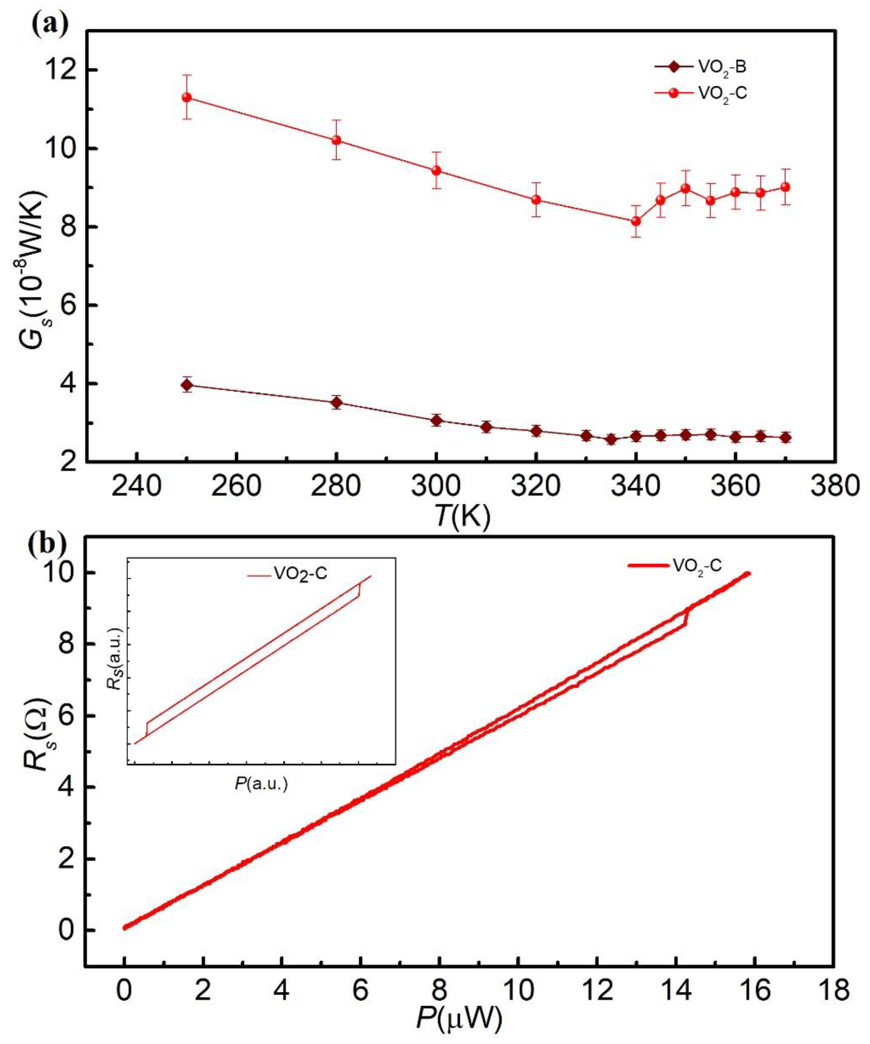
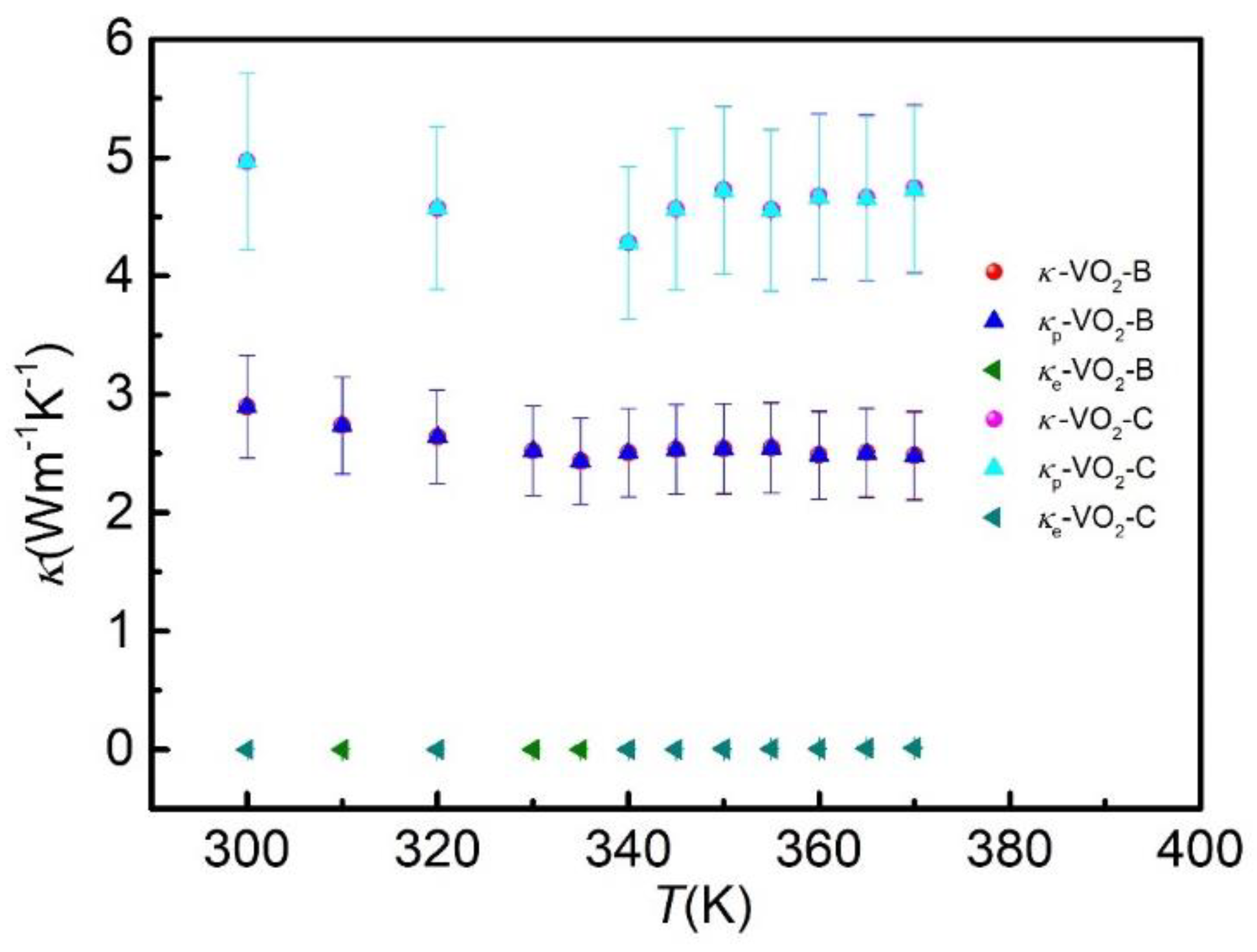
2. Results and Discussion

Monocrystalline VO2 nanowires were prepared via a variant of the vapor transport method reported previously [22]. Considering the effect of adhesion between VO2 nanowires and substrate, which may lead to the spontaneous formation of periodic, alternating M−I domain patterns along the VO2 nanowires’ length during MIT [23], single VO2 nanowire was transferred onto the suspended micro-electro-mechanical system (MEMS) device for thermal conductivity measurement using a tungsten needle in a micromanipulator (Imina Technologies Micromanipulation Platform). The MEMS device contains two thermally isolated thermometers for the measurement of thermal properties and four electrodes for the measurement of electrical properties and was suspended by the wet etching method. The inset in Figure 1b shows an exemplary scanning electron microscopy (SEM) image of the VO2 nanowire on the suspended MEMS device. To fix the VO2 nanowires, platinum (Pt) bars were deposited on the two ends of the VO2 nanowires by electron-beam induced deposition. The lengths of the VO2 nanowires changed from 11 µm to 20 µm, and their diameters ranged from 398 nm to 708 nm, labeled as VO2-A, VO2-B and VO2-C, respectively. The size parameters of the VO2 nanowires are displayed in Table 1.
Figure 1a shows the thermal conductance of VO2 nanowires versus temperature measured by the thermal bridge method. The overall measurement was performed in a high vacuum condition, better than 1 × 10⁻⁵ Pa. At a low temperature, the thermal conductance increased as the temperature increased, was mainly affected by phonon-boundary scattering and specific heat. The thermal conductance of VO2 nanowires reached a peak value of 2.14 × 10⁻⁷ W/K at T = 80 K for VO2-C. When the temperature was above 80 K, owing to phonon−phonon Umklapp scattering, the thermal conductance decreased as the temperature increased, and finally declined to 9.43 × 10⁻⁸ W/K at T = 300 K for VO2-C.
As the reciprocal of thermal conductance, the total thermal resistance (Rs) obtained from the thermal bridge method contains two parts: the intrinsic thermal resistance (Ri) of the suspended VO2 nanowires and the contact thermal resistance (Rc) between the VO2 nanowires and the electrodes (Pt). The analysis of the thermal conductance would be trivial without considering the contact thermal resistance. To further determine the result of the contact thermal resistance measured in the thermal bridge method, we measured it at room temperature directly by the electron-beam self-heating method [24,25,26]. The electron-beam self-heating method was developed on the basis of the suspended thermal bridge method, where the temperature change is monitored by the resistance change of two suspended thermometers, Rh and Rs. Different from the suspended thermal bridge method, the electron beam serves as the heat source in the electron-beam self-heating method. In general, the electron-beam can cause great damage to organic matter, and has little impact on inorganic matter [27,28]. In this work, the incident energy of the electron beam applied to the sample was 15 keV, which has been proven safe for VO2 nanowires in previous work [28]. The electron beam slowly scanned the entire VO2 nanowire, and its temperature slowly increased due to the electron beam power absorption. Subsequently, the heat transferred through the nanowire to the suspended thermometers, raising their temperature ΔTL and ΔTR, respectively. The heat conduction equations can be obtained respectively:
Δ T i ( x ) Δ T L R i ( x ) = Δ T L R b
Δ T i ( x ) Δ T R R T R i ( x ) = Δ T R R b
where Ri(x) is the total thermal resistance of VO2 nanowires from the start point to the focal point of the electron beam, ΔTi(x) is the temperature change at the focal point of the electron beam, RT and Rb are the total thermal resistance of the VO2 nanowires and the six beams of the suspended device, respectively. According to these two formulas, Ri(x) can be obtained:
R i ( x ) = R b { α 0 α i ( x ) 1 + α i ( x ) }
where α 0 = Δ T L 0 / Δ T R 0 , α i = Δ T L / Δ T R . ΔTL0 and ΔTR0 are the temperature change of the two thermometers in the suspended thermal bridge method, respectively. By measuring the thermal resistance when an electron beam scans along the nanowire, the thermal conductivity of the VO2 nanowires can be calculated as:
κ = 1 ( d R i d x ) · A
where A is the cross-sectional area of VO2 nanowires. Considering that the electron-beam self-heating method is carried out in SEM, it is usually applied to the measurement of thermal conductivity at room temperature.
Figure 1b shows the thermal resistance Ri of VO2 nanowires measured by the electron beam self-heating method as a function of scanning length at room temperature. The total measured intrinsic thermal resistance of VO2 nanowires is 2.97 × 10⁷ K/W at room temperature for VO2-A. The contact thermal resistance is obtained by subtracting the intrinsic thermal resistance from the total thermal resistance measured from the thermal bridge method. The contact thermal resistance was calculated to be 9.8 × 10⁶ K/W for VO2-A at room temperature. The contact thermal resistance accounted for 21~25% of total thermal resistance, indicating that the contact thermal resistance did indeed influence the thermal conductance of the VO2 nanowires. At low temperatures, the contact thermal resistance increased with increasing temperature. However, at high temperature, the contact thermal resistance increased and finally closed to an asymptotic value. Therefore, it is safe to assume that the contact thermal resistance at a higher temperature is similar to that at 300 K.
The thermal conductance of VO2 nanowires above room temperature are plotted in Figure 2a. Clearly, the thermal conductance dependence on temperature revealed that the samples underwent MIT [12]. The thermal conductance decreased with the increasing temperature under the phase transition temperature. Above the phase transition temperature, the VO2 nanowires were transformed into the metal phase and the thermal conductance increased as the temperature increased. The η is the ratio of the thermal conductivity change to the thermal conductivity in the I phase during the MIT, defined as η = ( κ I κ M ) / κ I , where κM and κI are the thermal conductivity in the M phase and I phase, respectively. The measured η is 4.12% in sample VO2–B. The η is smaller than that reported in VO2 films [10,12], which may be attributed to stronger boundary scattering. This result will be discussed in more detail later. The phase transition temperature is in the range of 335–340 K for bothVO2-B and VO2-C, lower than previous reports from electric measurement, probably due to the temperature rise during thermal measurement [29].
To understand more details of MIT, we modified the measurement method. The VO2 nanowires were fixed to the thermal bridge device, and the measurement temperature was set to be 335 K, slightly below MIT temperature. A DC current was applied to the heater, increasing from 0 to 150 µA, then gradually decreasing to 0. The temperature of the heater increased by nearly 27 K when the heating power reached the maximum of 15.89 μW. There was no doubt that the VO2 nanowires underwent MIT during the heating process since the resistance of the sensor had obviously jumped with the increase of heating power. As shown in Figure 2b, the resistance of the sensor jumped about 0.39 Ω with the increasing DC current at 335 K, which accounted for 3.95% of the total resistance variation. This behavior indicated great changes had taken place in the thermal conductance of the VO2 nanowires.
It is worth noting that the jump only occurred during the heating process, and the resistance displayed a linear behavior with the heating power during the cooling process. It is reasonable that a hysteresis should appear, as shown in insert of Figure 2b. However, in this measurement, the base temperature of VO2 nanowires is set to be 335 K, much higher than the phase transition temperature during the cooling process. Therefore, the jump in resistance of VO2 was not observed during the cooling process, which suggests that nanowires do not undergo MIT during the cooling process.
To further explore the characteristics of MIT, the electrical resistance of VO2 nanowires was measured by the four-electrode method from 300 K to 370 K. Figure 3 shows the temperature dependence of the electrical resistance during the cooling and heating process across the MIT. Consistent with the thermal conductance, the resistance exhibited a sharp jump across the MIT, which was over an order of magnitude. It is obvious that VO2 nanowires present the I phase at low temperature. However, it is pity to show that electrical resistance still decreased with increasing temperature at high temperature, similar to that in the I phase [30]. This was probably due to an incomplete MIT [31,32], where metal and insulator domains coexist in a single VO2 nanowire. In addition, the resistance apparently displayed a hysteresis during the temperature cycle, which is a prototypical signature of first-order MIT [33]. Notably, the hysteresis temperatures were 10 K and 7 K during the heating and cooling half cycle for VO2-B and VO2-C, respectively, which is consistent with the previous study [14]. The MIT temperatures were 347 K and 340 K for VO2-B and VO2-C, respectively, different from the result (341 K) previously reported, which may have arisen from the preparation of the sample. The four electrodes at both ends of the nanowire were deposited with Pt metal, which probably introduced a small amount of stress, resulting in the change of phase transition temperature of the VO2 nanowire [16,31].
To further analyze the underlying mechanisms, we studied the contribution of electronic thermal conductivity using the Wiedemann−Franz law: κ e = σ L T , where κe, σ, L and T are electronic thermal conductivity, electronic conductivity, Lorenz number and temperature of samples, respectively. Figure 4 shows the thermal conductivity as a function of temperature, where κp and κ were phonon thermal conductivity and measured total thermal conductivity, respectively. κp is determined by subtracting the κe from κ. It is evident that κe increases as the temperature rises over the entire temperature range. Remarkably, κe increased by two orders of magnitude near the phase transition point. However, the contribution of κe to κ was negligible, not exceeding 4%, no matter whether Wiedemann−Franz law was valid or not, as proposed previously [34]. κp decreased with the increasing temperature under the phase transition temperature. Above the phase transition temperature, the trend of temperature-dependence on thermal conductivity was reversed, i.e., κp gradually increased. The trend of κp was consistent with that of κ, indicating that the reason behind the jump of κ mainly comes from the contribution of phonons.
The measured η was only 4.12% and 5.68% for VO2-B and VO2-C, respectively. It was much smaller than that in the VO2 films which was up to 50% [10,12]. At higher temperature, i.e., in the metal state, the electrons played a dominate role in thermal conductivity, while κe was fully suppressed at insulating state [12]. This is the main reason to observe a great change in VO2 films. However, when VO2 films shrink to VO2 nanowires, both phonons and electrons are scattered by boundaries while electrons are much more severely scattered [35,36], because the electronic wave length is much larger than that in phonons, making κp dominate thermal conductivity even in the metal state. In our work, κtot was dominated by phonons and the contribution of the electrons was negligible in both the metal state and the insulating state. The η is consistent with a previous study in VO2 nanowires [11].
In low-dimensional materials, phonons are susceptible to boundary scattering because the size of the sample and the mean free path of phonons can be of the same order of magnitude [37,38]. In this work, the length of VO2-B and VO2-C was nearly the same, but with different diameters. The thermal conductivity of VO2-C was significantly higher than that of VO2-B, more than 70%. Therefore, the size effect may exist in VO2 nanowires. Similar behavior was also observed in other one-dimensional nanowires, such as silicon nanowires and zinc oxide nanowires [25,39,40,41], partially due to surface scattering and diameter-limited scattering. In addition, phonon scattering can be effectively improved by manipulating the structure of the nanomaterials such as nanoparticles [42,43], nanodots [44] and nanocomposite systems [45,46,47,48], which can lead to a series of interesting phonon transport phenomena. However, due to the limited number of samples, this result needs to be further studied.

3. Conclusions

In summary, the thermal conductance of VO2 nanowires was investigated in the temperature range of 15–370 K using the thermal bridge method. Through the phase transition from the insulator phase to metal phase, the thermal conductivity of the VO2 nanowire increased from 2.45 Wm−1K−1 to 2.55 Wm−1K−1, increasing by as much as 4.12%. Moreover, we found a size-dependent thermal conductivity in VO2 nanowires, where a thicker sample exhibited a higher thermal conductivity.

Author Contributions

Conceptualization, X.X.; methodology and formal analysis, D.L. and Q.W.; writing—original draft preparation, D.L.; writing—review and editing, D.L. and X.X. All authors have read and agreed to the published version of the manuscript.

Funding

The work was supported by the Key-Area Research and Development Program of Guangdong Province (No. 2020B010190004) and by the National Natural Science Foundation of China (No. 11890703, 11935010 and 12174286).

Data Availability Statement

The data presented in this study are available on request from the corresponding author.

Conflicts of Interest

The authors declare no conflict of interest.

References

  1. Morin, F.J. Oxides Which Show a Metal-to-Insulator Transition at the Neel Temperature. Phys. Rev. Lett. 1959, 3, 34–36. [Google Scholar] [CrossRef]
  2. Parikh, P.; Chakraborty, C.; Abhilash, T.S.; Sengupta, S.; Cheng, C.; Wu, J.; Deshmukh, M.M. Dynamically tracking the strain across the metal-insulator transition in VO2 measured using electromechanical resonators. Nano Lett. 2013, 13, 4685–4689. [Google Scholar] [CrossRef]
  3. Park, J.H.; Coy, J.M.; Kasirga, T.S.; Huang, C.; Fei, Z.; Hunter, S.; Cobden, D.H. Measurement of a solid-state triple point at the metal-insulator transition in VO2. Nature 2013, 500, 431–434. [Google Scholar] [CrossRef]
  4. Antunez, E.E.; Salazar-Kuri, U.; Estevez, J.O.; Campos, J.; Basurto, M.A.; Jiménez Sandoval, S.; Agarwal, V. Porous silicon-VO2 based hybrids as possible optical temperature sensor: Wavelength-dependent optical switching from visible to near-infrared range. J. Appl. Phys. 2015, 118, 134503. [Google Scholar] [CrossRef]
  5. Lim, H.; Stavrias, N.; Johnson, B.C.; Marvel, R.E.; Haglund, R.F.; McCallum, J.C. Optical switching and photoluminescence in erbium-implanted vanadium dioxide thin films. J. Appl. Phys. 2014, 115, 093107. [Google Scholar] [CrossRef]
  6. Li, S.Y.; Mlyuka, N.R.; Primetzhofer, D.; Hallén, A.; Possnert, G.; Niklasson, G.A.; Granqvist, C.G. Bandgap widening in thermochromic Mg-doped VO2 thin films: Quantitative data based on optical absorption. Appl. Phys. Lett. 2013, 103, 161907. [Google Scholar] [CrossRef] [Green Version]
  7. Pouget, J.P.; Launois, H.; D’Haenens, J.P.; Merenda, P.; Rice, T.M. Electron Localization Induced by Uniaxial Stress in Pure VO2. Phys. Rev. Lett. 1975, 35, 873–875. [Google Scholar] [CrossRef]
  8. Cavalleri, A.; Dekorsy, T.; Chong, H.H.W.; Kieffer, J.C.; Schoenlein, R.W. Evidence for a structurally-driven insulator-to-metal transition in VO2: A view from the ultrafast timescale. Phys. Rev. B 2004, 70, 161102. [Google Scholar] [CrossRef] [Green Version]
  9. Zheng, H.; Wagner, L.K. Computation of the correlated metal-insulator transition in vanadium dioxide from first principles. Phys. Rev. Lett. 2015, 114, 176401. [Google Scholar] [CrossRef] [PubMed]
  10. Oh, D.W.; Ko, C.; Ramanathan, S.; Cahill, D.G. Thermal conductivity and dynamic heat capacity across the metal-insulator transition in thin film VO2. Appl. Phys. Lett. 2010, 96, 151906. [Google Scholar] [CrossRef]
  11. Xie, R.; Bui, C.T.; Varghese, B.; Zhang, Q.; Sow, C.H.; Li, B.; Thong, J.T.L. An Electrically Tuned Solid-State Thermal Memory Based on Metal-Insulator Transition of Single-Crystalline VO2 Nanobeams. Adv. Funct. Mater. 2011, 21, 1602–1607. [Google Scholar] [CrossRef]
  12. Kizuka, H.; Yagi, T.; Jia, J.; Yamashita, Y.; Nakamura, S.; Taketoshi, N.; Shigesato, Y. Temperature dependence of thermal conductivity of VO2 thin films across metal–insulator transition. Jpn. J. Appl. Phys. 2015, 54, 053201. [Google Scholar] [CrossRef]
  13. Zhang, X.; Zhang, J.; Ke, F.; Li, G.; Ma, Y.; Liu, X.; Liu, C.; Han, Y.; Ma, Y.; Gao, C. Anomalous semiconducting behavior on VO2 under high pressure. RSC Adv. 2015, 5, 54843–54847. [Google Scholar] [CrossRef]
  14. Wu, J.; Gu, Q.; Guiton, B.S.; de Leon, N.P.; Ouyang, L.; Park, H. Strain-Induced Self Organization of Metal-Insulator Domains in Single-Crystalline VO2 Nanobeams. Nano Lett. 2006, 6, 2313–2317. [Google Scholar] [CrossRef]
  15. Bai, L.; Li, Q.; Corr, S.A.; Meng, Y.; Park, C.; Sinogeikin, S.V.; Ko, C.; Wu, J.; Shen, G. Pressure-induced phase transitions and metallization in VO2. Phys. Rev. B 2015, 91, 104110. [Google Scholar] [CrossRef] [Green Version]
  16. Atkin, J.M.; Berweger, S.; Chavez, E.K.; Raschke, M.B.; Cao, J.; Fan, W.; Wu, J. Strain and temperature dependence of the insulating phases of VO2 near the metal-insulator transition. Phys. Rev. B 2012, 85, 020101. [Google Scholar] [CrossRef] [Green Version]
  17. Lee, S.; Cheng, C.; Guo, H.; Hippalgaonkar, K.; Wang, K.; Suh, J.; Liu, K.; Wu, J. Axially engineered metal-insulator phase transition by graded doping VO2 nanowires. J. Am. Chem. Soc. 2013, 135, 4850–4855. [Google Scholar] [CrossRef]
  18. Kim, C.; Shin, J.S.; Ozaki, H. Effect of W doping in metal–insulator transition material VO2 by tunnelling spectroscopy. J. Phys. Condens. Matter 2007, 19, 096007. [Google Scholar] [CrossRef]
  19. Liu, K.; Fu, D.; Cao, J.; Suh, J.; Wang, K.X.; Cheng, C.; Ogletree, D.F.; Guo, H.; Sengupta, S.; Khan, A.; et al. Dense electron system from gate-controlled surface metal-insulator transition. Nano Lett. 2012, 12, 6272–6277. [Google Scholar] [CrossRef] [PubMed]
  20. Wei, J.; Ji, H.; Guo, W.; Nevidomskyy, A.H.; Natelson, D. Hydrogen stabilization of metallic vanadium dioxide in single-crystal nanobeams. Nat. Nanotechnol. 2012, 7, 357–362. [Google Scholar] [CrossRef]
  21. Yoon, H.; Choi, M.; Lim, T.W.; Kwon, H.; Ihm, K.; Kim, J.K.; Choi, S.Y.; Son, J. Reversible phase modulation and hydrogen storage in multivalent VO2 epitaxial thin films. Nat. Mater. 2016, 15, 1113–1119. [Google Scholar] [CrossRef] [PubMed]
  22. Guiton, B.S.; Gu, Q.; Prieto, A.L.; Gudiksen, M.S.; Park, H. Single-Crystalline Vanadium Dioxide Nanowires with Rectangular Cross Sections. J. Am. Chem. Soc. 2005, 127, 498–499. [Google Scholar] [CrossRef] [PubMed]
  23. Cao, J.; Fan, W.; Zheng, H.; Wu, J. Thermoelectric Effect across the Metal-Insulator Domain Walls in VO2 Microbeams. Nano Lett. 2009, 9, 4001–4006. [Google Scholar] [CrossRef] [PubMed]
  24. Wang, Q.; Liang, X.; Liu, B.; Song, Y.; Gao, G.; Xu, X. Thermal conductivity of V2O5 nanowires and their contact thermal conductance. Nanoscale 2020, 12, 1138–1143. [Google Scholar] [CrossRef]
  25. Wu, X.; Tao, Q.; Li, D.; Wang, Q.; Zhang, X.; Jin, H.; Li, J.; Wang, S.; Xu, X. Unprecedently low thermal conductivity of unique tellurium nanoribbons. Nano Res. 2021. [Google Scholar] [CrossRef]
  26. Aiyiti, A.; Bai, X.; Wu, J.; Xu, X.; Li, B. Measuring the thermal conductivity and interfacial thermal resistance of suspended MoS2 using electron beam self-heating technique. Sci. Bull. 2018, 63, 452–458. [Google Scholar] [CrossRef] [Green Version]
  27. Ferreira, A.; Xu, X.; Tan, C.-L.; Bae, S.-K.; Peres, N.M.R.; Hong, B.-H.; Özyilmaz, B.; Castro Neto, A.H. Transport properties of graphene with one-dimensional charge defects. EPL (Europhys. Lett.) 2011, 94, 28003. [Google Scholar] [CrossRef]
  28. Guo, H.; Wang, K.; Deng, Y.; Oh, Y.; Syed Asif, S.A.; Warren, O.L.; Shan, Z.W.; Wu, J.; Minor, A.M. Nanomechanical actuation from phase transitions in individual VO2 micro-beams. Appl. Phys. Lett. 2013, 102, 231909. [Google Scholar] [CrossRef] [Green Version]
  29. Fu, D.; Liu, K.; Tao, T.; Lo, K.; Cheng, C.; Liu, B.; Zhang, R.; Bechtel, H.A.; Wu, J. Comprehensive study of the metal-insulator transition in pulsed laser deposited epitaxial VO2 thin films. J. Appl. Phys. 2013, 113, 043707. [Google Scholar] [CrossRef] [Green Version]
  30. Allen, P.B.; Wentzcovitch, R.M.; Schulz, W.W.; Canfield, P.C. Resistivity of the high-temperature metallic phase of VO2. Phys. Rev. B 1993, 48, 4359–4363. [Google Scholar] [CrossRef] [PubMed]
  31. Cao, J.; Ertekin, E.; Srinivasan, V.; Fan, W.; Huang, S.; Zheng, H.; Yim, J.W.; Khanal, D.R.; Ogletree, D.F.; Grossman, J.C.; et al. Strain engineering and one-dimensional organization of metal-insulator domains in single-crystal vanadium dioxide beams. Nat. Nanotechnol. 2009, 4, 732–737. [Google Scholar] [CrossRef]
  32. Wei, J.; Wang, Z.; Chen, W.; Cobden, D.H. New aspects of the metal-insulator transition in single-domain vanadium dioxide nanobeams. Nat. Nanotechnol. 2009, 4, 420–424. [Google Scholar] [CrossRef] [PubMed] [Green Version]
  33. Ji, H.; Wei, J.; Natelson, D. Modulation of the electrical properties of VO2 nanobeams using an ionic liquid as a gating medium. Nano Lett. 2012, 12, 2988–2992. [Google Scholar] [CrossRef] [PubMed]
  34. Lee, S.; Hippalgaonkar, K.; Yang, F.; Hong, J.; Ko, C.; Suh, J.; Liu, K.; Wang, K.; Urban, J.J.; Zhang, X.; et al. Anomalously low electronic thermal conductivity in metallic vanadium dioxide. Science 2017, 355, 371–374. [Google Scholar] [CrossRef] [Green Version]
  35. Li, X.; Yan, Y.; Dong, L.; Guo, J.; Aiyiti1, A.; Xu, X.; Li, B. Thermal conduction across a boron nitride and SiO2 interface. J. Phys. D Appl. Phys. 2017, 50, 104002. [Google Scholar]
  36. Liu, D.; Chen, X.; Yan, Y.; Zhang, Z.; Jin, Z.; Yi, K.; Zhang, C.; Zheng, Y.; Wang, Y.; Yang, J.; et al. Conformal hexagonal-boron nitride dielectric interface for tungsten diselenide devices with improved mobility and thermal dissipation. Nat. Commun. 2019, 10, 1–11. [Google Scholar] [CrossRef] [Green Version]
  37. Wu, X.; Tang, W.; Xu, X. Recent progresses of thermal conduction in two-dimensional materials. Acta Phys. Sin. 2020, 69, 196602. [Google Scholar] [CrossRef]
  38. Xu, X.; Chen, J.; Li, B. Phonon thermal conduction in novel 2D materials. J. Phys. Condens. Matter 2016, 28, 483001. [Google Scholar] [CrossRef]
  39. Guo, J.; Huang, Y.; Wu, X.; Wang, Q.; Zhou, X.; Xu, X.; Li, B. Thickness-Dependent In-Plane Thermal Conductivity and Enhanced Thermoelectric Performance in p-Type ZrTe5 Nanoribbons. Phys. Status Solidi RRL 2019, 13, 1800529. [Google Scholar] [CrossRef]
  40. Yang, N.; Zhang, G.; Li, B. Violation of Fourier’s law and anomalous heat diffusion in silicon nanowires. Nano Today 2010, 5, 85–90. [Google Scholar] [CrossRef]
  41. Wang, X.; Gu, Y.; Sun, X.; Wang, H.; Zhang, Y. Third-order elastic constants of ZnO and size effect in ZnO nanowires. J. Appl. Phys. 2014, 115, 213516. [Google Scholar] [CrossRef]
  42. Jood, P.; Mehta, R.J.; Zhang, Y.; Peleckis, G.; Wang, X.; Siegel, R.W.; Borca-Tasciuc, T.; Dou, S.X.; Ramanath, G. Al-doped zinc oxide nanocomposites with enhanced thermoelectric properties. Nano Lett. 2011, 11, 4337–4342. [Google Scholar] [CrossRef]
  43. Wu, Z.; Xie, H.; Zhai, Y. Enhanced thermoelectric figure of merit in nanostructured ZnO by nanojunction effect. Appl. Phys. Lett. 2013, 103, 243901. [Google Scholar] [CrossRef]
  44. Nakamura, Y.; Isogawa, M.; Ueda, T.; Yamasaka, S.; Matsui, H.; Kikkawa, J.; Ikeuchi, S.; Oyake, T.; Hori, T.; Shiomi, J.; et al. Anomalous reduction of thermal conductivity in coherent nanocrystal architecture for silicon thermoelectric material. Nano Energy 2015, 12, 845–851. [Google Scholar] [CrossRef] [Green Version]
  45. Joshi, G.; Lee, H.; Lan, Y.; Wang, X.; Zhu, G.; Wang, D.; Gould, R.W.; Cuff, D.C.; Tang, M.Y.; Dresselhaus, M.S.; et al. Enhanced Thermoelectric Figure-of-Merit in Nanostructured p-type Silicon Germanium Bulk Alloys. Nano Lett. 2008, 8, 4670–4674. [Google Scholar] [CrossRef]
  46. Zebarjadi, M.; Joshi, G.; Zhu, G.; Yu, B.; Minnich, A.; Lan, Y.; Wang, X.; Dresselhaus, M.; Ren, Z.; Chen, G. Power factor enhancement by modulation doping in bulk nanocomposites. Nano Lett. 2011, 11, 2225–2230. [Google Scholar] [CrossRef]
  47. Tanusilp, S.; Ohishi, Y.; Muta, H.; Kurosaki, K. Synthesis and characterization of bulk Si–Ti nanocomposite and comparisons of approaches for enhanced thermoelectric properties in nanocomposites composed of Si and various metal silicides. J. Appl. Phys. 2020, 128, 095101. [Google Scholar] [CrossRef]
  48. Taniguchi, T.; Terada, T.; Komatsubara, Y.; Ishibe, T.; Konoike, K.; Sanada, A.; Naruse, N.; Mera, Y.; Nakamura, Y. Phonon transport in the nano-system of Si and SiGe films with Ge nanodots and approach to ultralow thermal conductivity. Nanoscale 2021, 13, 4971–4977. [Google Scholar] [CrossRef]
Figure 1. (a) Thermal conductance of the measured three VO2 nanowires as a function of temperature. (b) The intrinsic thermal resistance measured by the electron beam self-heating method varies with the scanning position of the electron beam for VO2-A. Inset: scanning electron microscopy images of the VO2 nanowires. The scale bar is 2 μm.
Nanomaterials 11 02428 g001
Figure 2. (a) The thermal conductance as a function of temperature for VO2-B and VO2-C, respectively. (b) The electrical resistance of the sensor as a function of the heating power using the thermal bridge method at T = 335 K. The inset shows the simulation results of electrical resistance of sensor as a function of the heating power in the thermal bridge method at T = 335 K.
Nanomaterials 11 02428 g002
Figure 3. The electrical resistance as a function of temperature for VO2-B and VO2-C, respectively.
Nanomaterials 11 02428 g003
Figure 4. The total thermal conductivity (κ, red circles and magenta circles), phonon thermal conductivity (κp, blue triangles and cyan triangles) and electronic thermal conductivity (κe, olive triangles and dark cyan triangles) of the VO2 nanowire samples as a function of temperature for VO2-B and VO2-C, respectively.
Nanomaterials 11 02428 g004
Table 1. Parameters of the VO2 nanowires used for the thermal conductance. The lengths and diameters of the VO2 nanowires were measured by SEM.
SampleLength (µm)Diameter (nm)κ (Wm−1K−1) @RTη Across MIT
VO2-A11.39398.12.32 ± 0.12-
VO2-B20.87530.73.06 ± 0.154.12%
VO2-C20.72708.44.96 ± 0.255.68%
Publisher’s Note: MDPI stays neutral with regard to jurisdictional claims in published maps and institutional affiliations.

