Article

A Novel Carbon-Assisted Chemical Vapor Deposition Growth of Large-Area Uniform Monolayer MoS2 and WS2

1
Department of Energy Systems Research, Ajou University, Suwon 16499, Korea
2
Department of Chemistry, Ajou University, Suwon 16499, Korea
*
Author to whom correspondence should be addressed.
Nanomaterials 2021, 11(9), 2423; https://doi.org/10.3390/nano11092423
Submission received: 17 August 2021 / Revised: 13 September 2021 / Accepted: 14 September 2021 / Published: 17 September 2021
(This article belongs to the Special Issue New Growth Mechanisms for Synthesizing Various Novel Nanostructures)

Abstract

:
Monolayer MoS2 can be used for various applications such as flexible optoelectronics and electronics due to its exceptional optical and electronic properties. For these applications, large-area synthesis of high-quality monolayer MoS2 is highly desirable. However, the conventional chemical vapor deposition (CVD) method using MoO3 and S powder has shown limitations in synthesizing high-quality monolayer MoS2 over a large area on a substrate. In this study, we present a novel carbon cloth-assisted CVD method for large-area uniform synthesis of high-quality monolayer MoS2. While the conventional CVD method produces thick MoS2 films in the center of the substrate and forms MoS2 monolayers at the edge of the thick MoS2 films, our carbon cloth-assisted CVD method uniformly grows high-quality monolayer MoS2 in the center of the substrate. The as-synthesized monolayer MoS2 was characterized in detail by Raman/photoluminescence spectroscopy, atomic force microscopy, and transmission electron microscopy. We reveal the growth process of monolayer MoS2 initiated from MoS2 seeds by synthesizing monolayer MoS2 with varying reaction times. In addition, we show that the CVD method employing carbon powder also produces uniform monolayer MoS2 without forming thick MoS2 films in the center of the substrate. This confirms that the large-area growth of monolayer MoS2 using the carbon cloth-assisted CVD method is mainly due to reducing properties of the carbon material, rather than the effect of covering the carbon cloth. Furthermore, we demonstrate that our carbon cloth-assisted CVD method is generally applicable to large-area uniform synthesis of other monolayer transition metal dichalcogenides, including monolayer WS2.

1. Introduction

Two-dimensional (2D) materials have attracted much attention due to their novel physical and chemical properties [1,2,3,4,5]. Graphene, the most studied 2D material, is thin, flexible, remarkably strong, and has exceptionally high electron mobility and thermal conductivity, allowing for a wide range of novel applications [1,2,6]. However, graphene has a zero bandgap, which results in very low on-off ratios in its applications of electronic devices such as transistors [4,5,7]. On the other hand, unlike graphene, transition metal dichalcogenides (TMDCs) have been intensively studied as new 2D layered materials because they have a sizable bandgap and interesting electronic and optical properties [3,4,5,7]. MoS2, a family of TMDCs, has been used as a building block for 2D field-effect transistors due to its high carrier mobility and excellent on-off ratios [8,9,10]. In addition, due to its exceptional physicochemical properties, 2D MoS2 has been extensively used for novel 2D electronics, flexible optoelectronics, and efficient catalysis [11,12,13,14,15]. When MoS2 is thinned down to a monolayer, its electronic structure and physical symmetries are radically altered, resulting in new physical behavior such as indirect to direct bandgap transitions [16,17,18]. In addition, monolayer MoS2 exhibits strong light–matter interactions due to its planar exciton confinement effect [16,19,20]. To increase the potential use of monolayer MoS2 in various applications, it is highly desirable to develop methods for preparing monolayer MoS2 [8,10,11,15,21,22]. The most well-known mechanical exfoliation method is suitable for producing high-quality single crystalline MoS2 flakes, but it cannot control the number of layers of the flakes and is unscalable for mass production [23,24,25,26]. In contrast, the chemical vapor deposition (CVD) method can control the number of MoS2 layers and enables wafer-scale synthesis [27,28,29]. However, the conventional CVD method using MoO3 and S powder has a problem in that thick MoS2 films are formed in the center of the substrate and only MoS2 monolayers are generated at the edge of the thick MoS2 films [30,31,32,33,34].
This problem is related to the growth mechanism of MoS2 in the conventional CVD method. The growth of MoS2 is mainly achieved by the reaction of S with suboxide MoO3-x species produced from MoO3 powder [35,36,37]. MoO3-x is highly volatile and improves the reaction kinetics for the formation of monolayer MoS2 [35,37]. Monolayer MoS2 can be effectively formed when the degree of MoO3-x formation is sufficiently high, whereas thick MoS2 films are generated when the degree of MoO3-x formation is low. Therefore, keeping the degree of MoO3-x formation high in the reaction process is a key condition for large-area uniform growth of high-quality monolayer MoS2 without forming thick MoS2 films. To achieve the large-area growth of monolayer MoS2, various methods have been reported, including confined-space CVD, reverse-flow chemical vapor epitaxy, inorganic vapor CVD, and metal organic CVD, etc. [38,39,40,41,42,43,44].
In this study, we report a novel carbon cloth-assisted CVD method that uniformly produces high-quality monolayer MoS2 over a large area on a substrate without forming thick MoS2 films. As-synthesized monolayer MoS2 was characterized in detail by Raman/photoluminescence (PL) spectroscopy, atomic force microscopy (AFM), and transmission electron microscopy (TEM). We reveal the detailed growth process of monolayer MoS2 initiated from MoS2 seeds by conducting a series of experiments with varying reaction times. In addition, we show that the CVD method employing carbon powder instead of carbon cloth also enables large-area growth of monolayer MoS2, confirming the large-area growth of monolayer MoS2 by the carbon cloth-assisted CVD method is mainly due to reducing properties of the carbon material, rather than the effect of covering the carbon cloth. Furthermore, we confirm that the carbon cloth-assisted CVD method can be used for the synthesis of other monolayer TMDCs such as monolayer WS2.

2. Materials and Methods

2.1. Conventional CVD Method for MoS2 and WS2 Synthesis

MoS2 was synthesized by a CVD method using a two-zone horizontal hot-wall tube furnace equipped with a mass flow controller and a vacuum pump (Edwards Vacuum, west Sussex, United Kingdom). The synthetic scheme is illustrated in Figure 1a. In a 1-inch diameter quartz tube, S powder (0.1 g, Sigma–Aldrich, St. Louis, MO, USA, 99.999%) in an alumina boat was placed upstream, and MoO3 powder (0.03 g, Sigma-Aldrich, 99.5%) in an alumina boat was put downstream. The growth promoter solution that was prepared by supersaturating NaCl in ethanol was dropped on a clean 300-nm SiO2/Si substrate and dried. NaCl serves as a promoter for the growth of MoS2 [45]. Na+ in NaCl can react with MoO3-x to form eutectic intermediates possessing a low melting point, promoting the growth of monolayer MoS2. The 300-nm SiO2/Si substrate was placed face down on the alumina boat containing MoO3 powder. We used a vacuum pump to lower the pressure of the quartz tube to 5-mTorr or less to remove air in the quartz tube before the reaction. After turning off the vacuum pump, Ar gas (ultra-high purity, 99.999%, Dong-A Gases, Seoul, Korea) flowed at a rate of 100 sccm until reaching atmospheric pressure. After the pressure reached the atmospheric pressure, Ar gas flowed at a rate of 10 sccm. The temperatures of S and MoO3 powder were independently controlled in two separate heating zones. The MoO3 powder was heated to 740 °C for 15 min at a rate of ≈47.6 °C min–1 and maintained at 740 °C for 20 min. The S powder was heated to 210 °C for 19 min at a rate of ≈9.7 °C min–1 and maintained at 210 °C for 16 min. After the end of the reactions, the furnace lid was opened to cool the furnace rapidly to room temperature.
For the synthesis of monolayer WS2, S powder (0.3 g, Sigma–Aldrich, 99.999%) and WO3 powder (0.05 g, Sigma–Aldrich, 99.9%) were used as precursors. The c-cut sapphire substrate was placed face down on an alumina boat containing WO3 powder. After the quartz tube was evacuated to 5-mTorr or less, Ar and H2 gases flowed at a rate of 140 sccm and 20 sccm, respectively, and the chamber pressure was maintained at ≈1.6 Torr. The WO3 powder was heated to 950 °C for 30 min at a rate of ≈30.8 °C/min and kept at 950 °C for 20 min. The S powder was heated to 210 °C for 32 min at a rate of ≈5.8 °C min–1 and maintained at 210 °C for 18 min.

2.2. Carbon Cloth-Assisted CVD Method for Monolayer MoS2 and WS2 Synthesis

The synthesis conditions of the carbon cloth-assisted CVD method are the same as those of the conventional CVD method described above, except that carbon cloth is placed on top of MoO3 and WO3 powder in an alumina boat for the synthesis of monolayer MoS2 and WS2, respectively.

2.3. Carbon Powder-Assisted CVD Method for Monolayer MoS2 Synthesis

The synthesis conditions of the carbon powder-assisted CVD method are the same as those of the conventional CVD synthesis method described above, except that activated carbon powder is mixed with MoO3 powder. The mixing ratios of MoO3 powder to activated carbon powder used in each experiment were 1:1, 1:2, 1:3, 1:4, 1:5, and 1:10, respectively.

2.4. Characterization

Raman spectra and maps were obtained using a 532-nm laser with 100 μW focused through a 100× objective at room temperature. Scanning electron microscopy (SEM) images and energy-dispersive X-ray spectroscopy (EDS) data were taken at 5 kV using a JSM-7900F (JEOL) microscope operating from 1 to 15 kV (JEOL Ltd., Tokyo, Japan). AFM measurement was performed in noncontact mode on an Anton–Paar Tosca 400 AFM instrument (Anton Paar, Sumida, Austria). TEM measurements were performed using a JEM-2100F microscope (JEOL Ltd., Tokyo, Japan).

3. Results and Discussion

3.1. Thick MoS2 Films and Monolayer MoS2 Synthesized Using the Conventional CVD Method

Figure 1a shows a schematic illustration of the experimental setup for the conventional CVD method in which solid powders (MoO3 and S powder) are used as precursors for MoS2 synthesis. Figure 1b shows an optical image of MoS2 synthesized on a 300-nm SiO2/Si substrate using the conventional CVD method. Figure 1c is a magnified optical image of region A in Figure 1b, showing the MoS2 grown in the form of a thick film in the center of the substrate. Figure 1d is a magnified optical image of region B in Figure 1b, showing the edge region of the thick MoS2 films. Figure 1e,f show magnified optical images of the dotted red rectangle and dotted blue rectangle in Figure 1d, respectively, confirming the partial formation of monolayer MoS2 at the edge of the thick MoS2 film. Additional data on the optical characterization of the MoS2 grown using the conventional CVD method are shown in Supplementary Materials Figure S1. The growth of such thick MoS2 films and partial formation of monolayer MoS2 have been commonly observed in MoS2 growth by the conventional CVD method using MoO3 and S powder as precursors [30,31,32,33,34]. An AFM height image of monolayer MoS2 shows small particles grown nonuniformly on the surface of monolayer MoS2 (Figure 1g). The line profile obtained along the dotted red line in Figure 1g shows that the thickness of the synthesized monolayer MoS2 is ~0.72 nm, which is consistent with the reported thickness of monolayer MoS2 (Figure 1h) [19,46].
Raman and photoluminescence (PL) analyses were performed on the as-synthesized monolayer MoS2. The Raman spectrum of monolayer MoS2 shows that the frequency difference between the E12g mode located at 382 cm−1 and the A1g mode located at 403 cm−1 was approximately 21 cm−1 (Figure 1i), which is consistent with that of the reported monolayer MoS2 [31]. Due to the direct bandgap of monolayer MoS2, the PL spectrum of MoS2 shows a strong A exciton peak at 1.84 eV (Figure 1j) [19,47]. Raman and PL maps show that monolayer MoS2 exhibited nonuniform Raman and PL peak intensities, confirming that monolayer MoS2 had nonuniform optical and electronic properties (Figure 1k–m). Even when H2 was used as a carrier gas with Ar for the MoS2 synthesis, thick MoS2 films were formed in the center of the substrate and some flakes of monolayer MoS2 were partially formed at the edge of the thick films (Figure S2).

3.2. Monolayer MoS2 Synthesized Using Carbon Cloth-Assisted CVD Method

Figure 2a shows a schematic illustration of the carbon cloth-assisted CVD growth of monolayer MoS2. The experimental conditions were the same as those of the conventional CVD synthesis growth, except that the MoO3 powder contained in the alumina boat was covered with carbon cloth. Unlike the conventional CVD method, this carbon cloth-assisted CVD method enables the growth of monolayer MoS2 without forming thick films in the center of the substrate. Figure 2b is an optical image showing MoS2 grown on a 300-nm SiO2/Si substrate by the carbon cloth-assisted CVD method, confirming that there were no thick films in the center of the substrate. Figure 2c–e show the low-magnification and high-magnification optical images for regions A, B, and C in Figure 2b, respectively, confirming that monolayer MoS2 grew relatively uniformly throughout the substrate without forming thick MoS2 films in the center of the substrate. Additional data on the optical characterization of the MoS2 grown using the carbon-assisted CVD method are shown in Figures S3 and S4. In addition, we observed that the size of the monolayer MoS2 decreased when we moved from region A to region C in Figure 2b. The change in the size of the monolayer MoS2 can be explained as follows; on regions A and B located upstream, a sufficient amount of S vapor reacts with MoO3-x to form large monolayer MoS2, whereas on region C located downstream, the amount of S vapor reaching region C is relatively small, resulting in relatively limited reactions with S vapor and MoO3-x.
To investigate the mechanisms of the carbon cloth-assisted CVD growth of monolayer MoS2, materials formed on carbon cloth during the growth were analyzed. Figure 3a,b show low-magnification and high-magnification SEM images of carbon cloth obtained after the carbon cloth-assisted CVD growth, respectively, confirming that the surface of the carbon cloth was entirely covered with nanoplates with a size of two to three microns. Raman analysis confirms that these nanoplates consisted of MoS2 and MoO2 (Figure 3c) [48]. In addition, EDS analysis shows that the nanoplates were composed of Mo, S, and O, and the proportion of O was very large compared to the proportion of S (Figure 3d), which confirms that the nanoplates were mostly composed of MoO2 and were partially composed of MoS2. MoO2 is a byproduct that is frequently formed in the conventional CVD growth of MoS2 using MoO3 and S powder as precursors. MoO2 is nonvolatile and has a high melting point, so it remains once it is formed on the substrate. One of the important roles of carbon cloth in carbon cloth-assisted CVD growth is to prevent MoO2 from forming on the SiO2/Si substrate by allowing MoO2 to form on the carbon cloth (Figure S5). Another role of carbon cloth is to improve the reaction kinetics for MoS2 growth by facilitating the formation of suboxide MoO3-x species formed from MoO3, as carbon acts as a reducing agent.
Figure 4a is an AFM image of the monolayer MoS2 synthesized using the carbon cloth-assisted CVD method, which shows that the surface of monolayer MoS2 was clean without any particles, unlike monolayer MoS2 synthesized using the conventional CVD method. The line profile obtained along the dotted red line in Figure 4a shows that the thickness of the synthesized monolayer MoS2 was ~0.988 nm, which is consistent with the reported thickness of monolayer MoS2 (Figure 4b) [19,46]. Additional AFM data of monolayer MoS2 are shown in Figure S6. Figure 4c shows an optical image of monolayer MoS2 grown on an SiO2/Si substrate. The Raman spectrum (Curve 1) of monolayer MoS2 taken at point 1 shows the Raman peaks of the E12g mode located at 380 cm−1 and the A1g mode located at 401 cm−1 (Figure 4d) [31]. Curve 2 in Figure 4d shows the Raman spectrum obtained from the substrate at point 2. The PL spectrum (Curve 1) of monolayer MoS2 shows a strong peak at 1.84 eV (Figure 4e), which is consistent with the A exciton peak due to the direct bandgap of monolayer MoS2 [19,47]. Curve 2 in Figure 4e is the PL spectrum obtained from the substrate at point 2. Raman and PL maps of MoS2 show that monolayer MoS2 exhibited uniform Raman and PL peak intensities, confirming that monolayer MoS2 had a uniform chemical composition and electronic structure (Figure 4f–h). Figure 4i shows a TEM image of monolayer MoS2. The high-resolution TEM (HRTEM) image (Figure 4j) and corresponding selected area electron diffraction (SAED) patterns (Figure 4k) with [001] zone axis confirm the hexagonal lattice structure with the lattice spacing of 0.278 nm assigned to the (100) planes of MoS2. In addition, TEM–EDS analysis shows that the monolayer MoS2 consisted of Mo and S, and the ratio of Mo to S elements was 1:2 (Figure 4l). The Cu peak originated from the TEM grid, and the Cr peak came from the pole pieces of the TEM.
Figure 5 shows the growth process of monolayer MoS2 depending on the reaction time in carbon cloth-assisted CVD growth. The reaction time was set to 5, 15, 20, and 25 min, respectively. Figure 5a–d show the low-magnification and high-magnification optical images of MoS2 flakes synthesized at each reaction time. At the reaction time of five minutes, small round-shaped MoS2 seeds were formed (Figure 5a). At the reaction times of 15 and 20 min, triangular monolayer MoS2 was generated, and its size increased with increasing reaction time (Figure 5b,c). Size distribution of monolayer MoS2 synthesized at reaction times of 5 min, 15 min, and 20 min is shown in Figure S7. At the reaction time of 25 min, monolayer MoS2 films were formed (Figure 5d). The growth of monolayer MoS2 depending on the reaction time can be explained as follows. In the initial stage of the reaction (reaction time: five minutes), S vapor and MoO3-x vapor are supplied on the substrate to form small MoS2 seeds. As the reaction time increases (reaction time: 15 and 20 min), MoS2 seeds form on the substrate and grow to form triangular monolayer MoS2, and as the reaction time increases, the size of the monolayer MoS2 increases. When the reaction time is further increased (reaction time: 25 min), S vapor and MoO3-x vapor are continuously supplied to grow triangular monolayer MoS2 to form monolayer MoS2 films. Figure 5e shows the Raman spectra of MoS2 synthesized at each reaction time, confirming that the flakes and films synthesized at all reaction times were composed of MoS2. Figure 5f shows the PL spectra of MoS2 formed at each reaction time, confirming that all MoS2, except for the MoS2 seeds formed at the reaction time of five minutes, exhibited a strong A exciton peak at 1.84 eV, indicating that the as-synthesized MoS2 flakes and layers were monolayers. We believe that the variation of the PL peak position originated from the variation of strain or defects of the as-synthesized monolayer MoS2 [49].

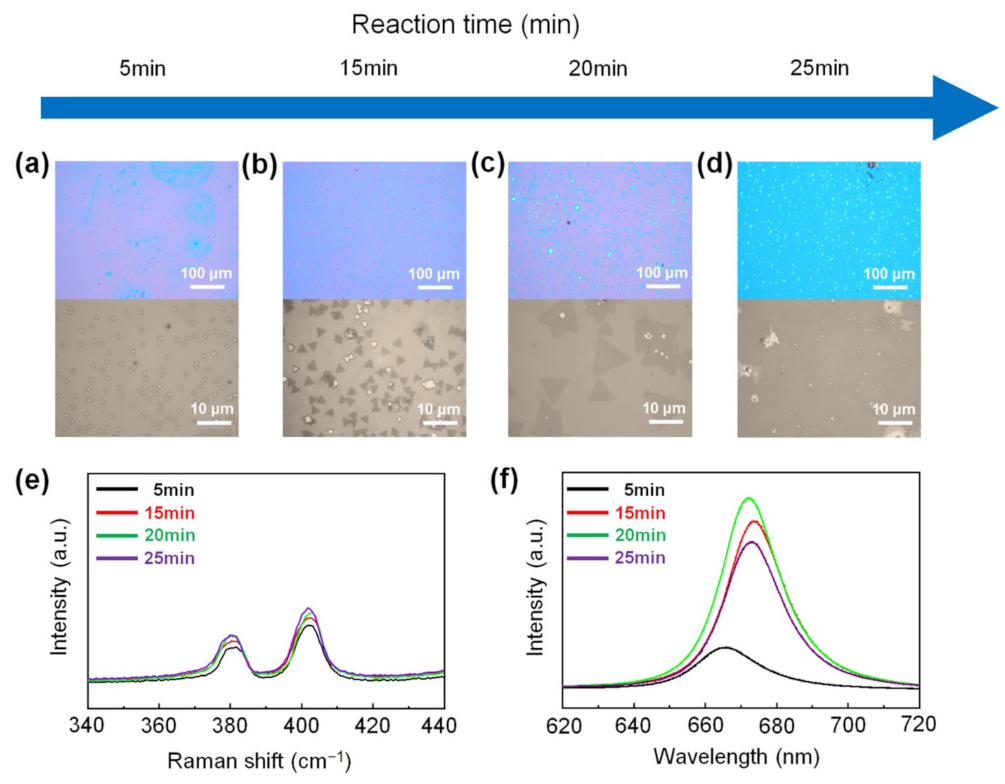
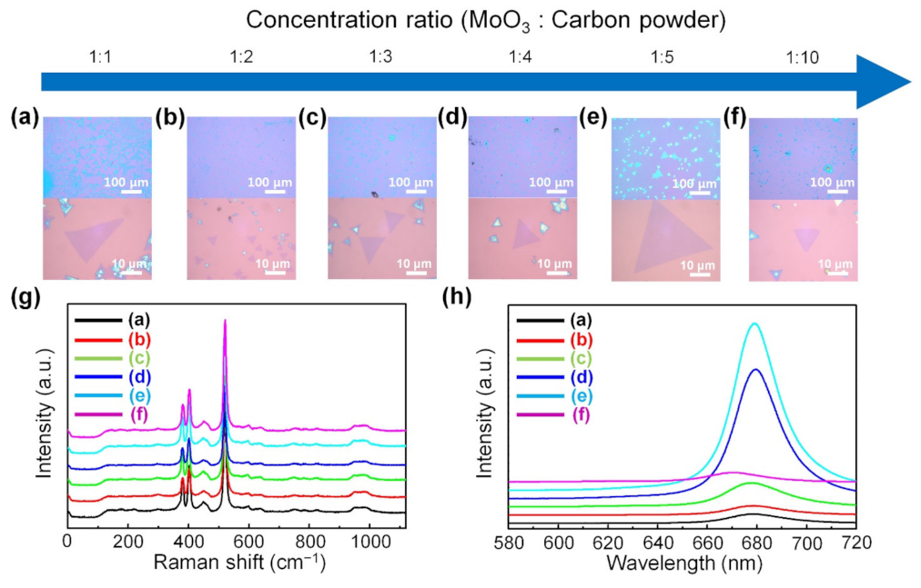
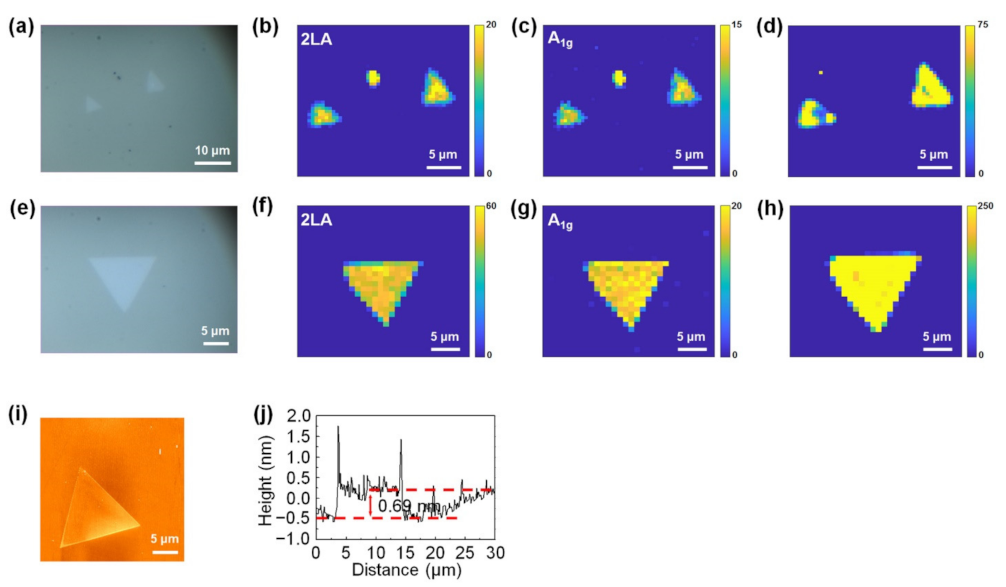
3.3. Monolayer MoS2 Synthesized Using the Carbon Powder-Assisted CVD Method

The MoS2 synthesis was conducted using the carbon powder-assisted CVD method to determine whether the large-area growth of monolayer MoS2 without forming thick MoS2 films is because carbon acts as a reducing agent or because carbon cloth physically covers the MoO3 precursor. For carbon powder-assisted CVD synthesis, experiments were conducted by mixing MoO3 powder and carbon powder in ratios of 1:1, 1:2, 1:3, 1:4, 1:5, and 1:10, respectively.
Figure 6a–f shows low-magnification and high-magnification optical images of monolayer MoS2 synthesized with various mixing ratios of carbon powder to MoO3 powder, confirming that monolayer MoS2 was grown on the substrate over the large area without forming thick films in the center of the substrate. We demonstrated that the carbon material, acting as a reducing agent, plays an important role in the large-area uniform synthesis of monolayer MoS2. When the mixing ratio of MoO3 powder to carbon powder was 1:1, the MoS2 had a nonequilateral triangle shape, which means that MoS2 has low crystallinity (Figure 6a). This is because when the ratio of carbon powder is low, the degree of the formation of suboxide MoO3-x species formed during the reaction process is low, so the reaction kinetics deteriorate. When the mixing ratio of the MoO3 powder to the carbon powder was from 1:2 to 1:10, MoS2 with an equilateral triangle shape and high crystallinity was formed. Among them, the largest monolayer MoS2 was obtained when the mixing ratio of MoO3 powder to carbon powder was 1:5 (Figure 6e). When the mixing ratio of the MoO3 powder to the carbon powder was further changed to 1:10, the size of the monolayer MoS2 became small (Figure 6f).
The Raman spectra confirm that all synthesized flakes exhibited Raman peaks at the E12g mode and the A1g mode of MoS2 (Figure 6g). Figure 6h shows the PL spectra of the MoS2 synthesized with various mixing ratios of carbon powder to MoO3 powder. As the ratio of carbon powder increased, monolayer MoS2 with higher crystallinity was produced, which showed higher PL intensity. The PL spectra of the MoS2 show strong A exciton peaks at 1.84 eV when the mixing ratio of MoO3 powder to carbon powder was 1:4 and 1:5, confirming that the as-synthesized MoS2 flakes were high-quality MoS2 monolayers. However, when the ratio of carbon powder to MoO3 powder is too high, MoO3 is reduced to suboxide MoO3-x species and further reduced to form MoO2 or Mo, which rather hinders the growth of monolayer MoS2. Thus, under this condition, the size of the monolayer MoS2 became smaller again and the PL intensity decreased.
We performed the synthesis of monolayer MoS2 using graphite powder mixed with MoO3 powder (Figure S8). Like the activated carbon powder-assisted CVD method, the graphite powder-assisted CVD method led to the synthesis of monolayer MoS2 over a large area on the substrate. These results confirm that the reducing property of carbon is the main factor inducing the large-area growth of monolayer MoS2.

3.4. Growth Mechanism of Monolayer MoS2 in the Carbon-Assisted CVD Growth

During the carbon-assisted CVD growth of monolayer MoS2, MoO3 is reduced by carbon to form volatile suboxide MoO3−x species, which are further sulfurized to form MoS2 on an SiO2/Si substrate. The proposed reaction mechanism is as follows [50,51].
2MoO3 + xC → 2MoO3−x + xCO2
2MoO3−x + (7 − x)S → 2MoS2 + (3 − x)SO2
In this paper, we showed that the reaction kinetics for the growth of monolayer MoS2 can be improved by using carbon materials. When no carbon materials were used, thick MoS2 films were formed in most areas on the substrate and Figure S1), whereas when carbon materials were used, monolayer MoS2 was formed in most areas on the substrate (Figure 2, Figure 6 and Figure S3). Thus, we believe that the carbon materials improve the reaction kinetics for the growth of monolayer MoS2 and suppress the formation of thick MoS2 films.
The generally accepted mechanism for the growth of monolayer MoS2 involves the nucleation of tiny suboxide MoO3-x seeds on the substrate surface followed by subsequent sulfurization of these seeds and subsequent growth of monolayer MoS2 [50]. Thus, suboxide MoO3-x species play a key role in the growth of monolayer MoS2. By using carbon cloth or carbon powder, we effectively increased the degree of the formation of suboxide MoO3-x species, leading to the growth of monolayer MoS2 in most areas on the substrate. On the other hand, the formation of thick MoS2 films can be achieved by either the direct nucleation of nonvolatile MoO3 or MoO2 clusters on the substrate followed by subsequent sulfurization.

3.5. Application to Other TMDCs

In addition, to confirm that the carbon cloth-assisted CVD method applies to the synthesis of other monolayer TMDCs, we performed the synthesis of monolayer WS2 using the conventional CVD method and the carbon cloth-assisted CVD method, respectively. Figure 7a is an optical image of the monolayer WS2 synthesized using the conventional CVD method. The size of the monolayer WS2 was as small as four microns, and its shape was not an equilateral triangle. Raman and PL mappings at the 2LA mode and A1g mode of WS2 show that the monolayer WS2 exhibited nonuniform Raman and PL peak intensities, confirming that the monolayer WS2 had nonuniform optical and electronic properties (Figure 7b–d). Figure 7e is an optical image of monolayer WS2 synthesized using the carbon cloth-assisted CVD method. The size of the monolayer WS2 was approximately 13.5 microns, and its shape was an equilateral triangle. Raman and PL mappings at the 2LA mode and A1g mode of WS2 show that the monolayer WS2 exhibited uniform Raman and PL peak intensities, confirming that monolayer WS2 had a uniform chemical composition and electronic structure (Figure 7f–h). Figure 7i shows an AFM image of the monolayer WS2 synthesized using the carbon cloth-assisted CVD method, confirming that the surface of the monolayer WS2 was clean without any particles. The line profile shows that the thickness of the monolayer WS2 was ~0.69 nm, which is consistent with the reported thickness of the monolayer WS2 (Figure 7j) [52,53].
The growth of high-quality monolayer WS2 by the carbon cloth-assisted CVD method can be explained as follows. For the synthesis of monolayer WS2, WO3 powder was used as a precursor. The WO3 has a significantly high melting point (1473 °C) and its vapor pressure is very low at the reaction temperature (950 °C). Thus, the conventional CVD method produces small monolayer flakes of WS2 with very low coverage on the substrate (Figure S9). When carbon cloth is placed on top of WO3 powder, carbon acts as a reducing agent and increases the degree of the formation of suboxide WO3-x species to improve the reaction kinetics for the formation of monolayer WS2. Thus, under this condition, triangular monolayer WS2 with increased size forms uniformly on the substrate (Figure S9). Consequently, we confirmed that the carbon cloth-assisted CVD method is generally applicable to the synthesis of high-quality monolayer WS2.

4. Conclusions

We developed a novel carbon-assisted CVD method for large-area uniform growth of high-quality monolayer MoS2. Using the carbon cloth-assisted CVD method, we synthesized high-quality monolayer MoS2 uniformly over a large area on the substrate without forming thick MoS2 films. Through detailed analyses of the carbon cloth that was used in the reaction and experiments with varying reaction times, we revealed the mechanisms for the large-area growth of high-quality monolayer MoS2. In addition, we showed that the carbon powder-assisted CVD method also produces high-quality monolayer MoS2 over a large area on the substrate. This confirms that the uniform large-area growth of MoS2 using the carbon cloth-assisted CVD method is mainly due to the reducing properties of the carbon material. Furthermore, we demonstrated that the carbon cloth-assisted CVD method can be generally used to synthesize monolayer WS2.

Supplementary Materials

The following are available online at https://www.mdpi.com/article/10.3390/nano11092423/s1, Figure S1: Additional optical characterization of the MoS2 grown using the conventional CVD method, Figure S2: MoS2 synthesized by the CVD method using H2 as a carrier gas with Ar, Figure S3: Additional optical characterization of the MoS2 grown using the carbon cloth-assisted CVD method, Figure S4: MoS2 flakes grown using the carbon cloth-assisted CVD growth, Figure S5: MoO2-MoS2 nanoplates grown after the carbon cloth-assisted CVD growth and after the conventional CVD growth, Figure S6: Additional AFM data of monolayer MoS2 synthesized using the carbon cloth-assisted CVD method, Figure S7: Size distribution of monolayer MoS2 synthesized at reaction times of 5 min, 15 min, and 20 min using the carbon cloth-assisted CVD method, respectively, Figure S8: Graphite powder-assisted CVD growth of monolayer MoS2, Figure S9: Monolayer WS2 synthesized on a c-cut sapphire substrate using the conventional CVD method and the carbon cloth-assisted CVD method.

Author Contributions

Conceptualization, Y.Y.; investigation, J.B. and Y.Y.; writing—original draft preparation, J.B. and Y.Y.; writing—review and editing, Y.Y.; supervision, Y.Y.; funding acquisition, Y.Y. All authors have read and agreed to the published version of the manuscript.

Funding

This work was supported by the National Research Foundation of Korea (NRF) grant funded by the Korea government (MSIT) (2019R1C1C1008070 and 2018R1C1B5044670). This work was supported by Institute of Information & communications Technology Planning & Evaluation (IITP) grant funded by the Korea government (MSIT) (2021-0-00185). This research was supported by Basic Science Research Program through the National Research Foundation of Korea (NRF) funded by the Ministry of Education (2021R1A6A1A10044950). This research was supported by Nano·Material Technology Development Program through the NRF funded by the MSIT (2009-0082580).

Conflicts of Interest

The authors declare no conflict of interest.

References

  1. Geim, A.K.; Novoselov, K.S. The rise of graphene. Nat. Mater. 2007, 6, 183–191. [Google Scholar] [CrossRef]
  2. Neto, A.C.; Guinea, F.; Peres, N.M.; Novoselov, K.S.; Geim, A.K. The electronic properties of graphene. Rev. Mod. Phys. 2009, 81, 109. [Google Scholar] [CrossRef] [Green Version]
  3. Wilson, J.A.; Yoffe, A. The transition metal dichalcogenides discussion and interpretation of the observed optical, electrical and structural properties. Adv. Phys. 1969, 18, 193–335. [Google Scholar] [CrossRef]
  4. Wang, Q.H.; Kalantar-Zadeh, K.; Kis, A.; Coleman, J.N.; Strano, M.S. Electronics and optoelectronics of two-dimensional transition metal dichalcogenides. Nat. Nanotechnol. 2012, 7, 699–712. [Google Scholar] [CrossRef] [PubMed]
  5. Manzeli, S.; Ovchinnikov, D.; Pasquier, D.; Yazyev, O.V.; Kis, A. 2D transition metal dichalcogenides. Nat. Rev. Mater. 2017, 2, 1–15. [Google Scholar] [CrossRef]
  6. Allen, M.J.; Tung, V.C.; Kaner, R.B. Honeycomb carbon: A review of graphene. Chem. Rev. 2010, 110, 132–145. [Google Scholar] [CrossRef]
  7. Mak, K.F.; Shan, J. Photonics and optoelectronics of 2D semiconductor transition metal dichalcogenides. Nat. Photonics 2016, 10, 216–226. [Google Scholar] [CrossRef]
  8. Radisavljevic, B.; Radenovic, A.; Brivio, J.; Giacometti, V.; Kis, A. Single-layer MoS2 transistors. Nat. Nanotechnol. 2011, 6, 147–150. [Google Scholar] [CrossRef]
  9. Li, H.; Yin, Z.; He, Q.; Li, H.; Huang, X.; Lu, G.; Fam, D.W.H.; Tok, A.I.Y.; Zhang, Q.; Zhang, H. Fabrication of single-and multilayer MoS2 film-based field-effect transistors for sensing NO at room temperature. Small 2012, 8, 63–67. [Google Scholar] [CrossRef]
  10. Vaknin, Y.; Dagan, R.; Rosenwaks, Y. Schottky Barrier Height and Image Force Lowering in Monolayer MoS2 Field Effect Transistors. Nanomaterials 2020, 10, 2346. [Google Scholar] [CrossRef]
  11. Lopez-Sanchez, O.; Lembke, D.; Kayci, M.; Radenovic, A.; Kis, A. Ultrasensitive photodetectors based on monolayer MoS2. Nat. Nanotechnol. 2013, 8, 497–501. [Google Scholar] [CrossRef] [PubMed]
  12. Kim, S.; Park, W.; Kim, D.; Kang, J.; Lee, J.; Jang, H.Y.; Song, S.H.; Cho, B.; Lee, D. Novel Exfoliation of High-Quality 2H-MoS2 Nanoflakes for Solution-Processed Photodetector. Nanomaterials 2020, 10, 1045. [Google Scholar] [CrossRef]
  13. Li, H.; Tsai, C.; Koh, A.L.; Cai, L.; Contryman, A.W.; Fragapane, A.H.; Zhao, J.; Han, H.S.; Manoharan, H.C.; Abild-Pedersen, F.; et al. Activating and optimizing MoS2 basal planes for hydrogen evolution through the formation of strained sulphur vacancies. Nat. Mater. 2016, 15, 48–53. [Google Scholar] [CrossRef] [PubMed]
  14. Huang, P.C.; Wu, C.L.; Brahma, S.; Shaikh, M.O.; Huang, J.L.; Lee, J.J.; Wang, S.C. MoS2-Carbon Inter-overlapped Structures as Effective Electrocatalysts for the Hydrogen Evolution Reaction. Nanomaterials 2020, 10, 1389. [Google Scholar] [CrossRef] [PubMed]
  15. Zhang, J.; Wu, J.; Guo, H.; Chen, W.; Yuan, J.; Martinez, U.; Gupta, G.; Mohite, A.; Ajayan, P.M.; Lou, J. Unveiling active sites for the hydrogen evolution reaction on monolayer MoS2. Adv. Mater. 2017, 29, 1701955. [Google Scholar] [CrossRef] [PubMed]
  16. Mak, K.F.; Lee, C.; Hone, J.; Shan, J.; Heinz, T.F. Atomically thin MoS2: A new direct-gap semiconductor. Phys. Rev. Lett. 2010, 105, 136805. [Google Scholar] [CrossRef] [Green Version]
  17. Steinhoff, A.; Kim, J.H.; Jahnke, F.; Rosner, M.; Kim, D.S.; Lee, C.; Han, G.H.; Jeong, M.S.; Wehling, T.O.; Gies, C. Efficient Excitonic Photoluminescence in Direct and Indirect Band Gap Monolayer MoS2. Nano Lett. 2015, 15, 6841–6847. [Google Scholar] [CrossRef]
  18. Niu, Y.; Gonzalez-Abad, S.; Frisenda, R.; Marauhn, P.; Drüppel, M.; Gant, P.; Schmidt, R.; Taghavi, N.S.; Barcons, D.; Molina-Mendoza, A.J.; et al. Thickness-Dependent Differential Reflectance Spectra of Monolayer and Few-Layer MoS2, MoSe2, WS2 and WSe2. Nanomaterials 2018, 8, 725. [Google Scholar] [CrossRef] [Green Version]
  19. Splendiani, A.; Sun, L.; Zhang, Y.; Li, T.; Kim, J.; Chim, C.Y.; Galli, G.; Wang, F. Emerging photoluminescence in monolayer MoS2. Nano Lett. 2010, 10, 1271–1275. [Google Scholar] [CrossRef]
  20. Liu, X.; Galfsky, T.; Sun, Z.; Xia, F.; Lin, E.-c.; Lee, Y.-H.; Kéna-Cohen, S.; Menon, V.M. Strong light–matter coupling in two-dimensional atomic crystals. Nat. Photonics 2015, 9, 30–34. [Google Scholar] [CrossRef]
  21. Yin, Z.; Li, H.; Li, H.; Jiang, L.; Shi, Y.; Sun, Y.; Lu, G.; Zhang, Q.; Chen, X.; Zhang, H. Single-layer MoS2 phototransistors. ACS Nano 2012, 6, 74–80. [Google Scholar] [CrossRef] [PubMed] [Green Version]
  22. Zhang, W.; Huang, J.K.; Chen, C.H.; Chang, Y.H.; Cheng, Y.J.; Li, L.J. High-gain phototransistors based on a CVD MoS2 monolayer. Adv. Mater. 2013, 25, 3456–3461. [Google Scholar] [CrossRef] [PubMed]
  23. Li, H.; Wu, J.; Yin, Z.; Zhang, H. Preparation and applications of mechanically exfoliated single-layer and multilayer MoS2 and WSe2 nanosheets. Acc. Chem. Res. 2014, 47, 1067–1075. [Google Scholar] [CrossRef] [PubMed]
  24. Yi, M.; Shen, Z. A review on mechanical exfoliation for the scalable production of graphene. J. Mater. Chem. A 2015, 3, 11700–11715. [Google Scholar] [CrossRef]
  25. Zeng, Z.; Yin, Z.; Huang, X.; Li, H.; He, Q.; Lu, G.; Boey, F.; Zhang, H. Single-layer semiconducting nanosheets: High-yield preparation and device fabrication. Angew. Chem. 2011, 50, 11093–11097. [Google Scholar] [CrossRef]
  26. Dumcenco, D.; Ovchinnikov, D.; Marinov, K.; Lazic, P.; Gibertini, M.; Marzari, N.; Lopez Sanchez, O.; Kung, Y.C.; Krasnozhon, D.; Chen, M.W.; et al. Large-Area Epitaxial Monolayer MoS2. ACS Nano 2015, 9, 4611–4620. [Google Scholar] [CrossRef]
  27. Cai, Z.; Liu, B.; Zou, X.; Cheng, H.-M. Chemical vapor deposition growth and applications of two-dimensional materials and their heterostructures. Chem. Rev. 2018, 118, 6091–6133. [Google Scholar] [CrossRef]
  28. Wang, X.; Feng, H.; Wu, Y.; Jiao, L. Controlled synthesis of highly crystalline MoS2 flakes by chemical vapor deposition. J. Am. Chem. Soc. 2013, 135, 5304–5307. [Google Scholar] [CrossRef]
  29. Lee, Y.H.; Zhang, X.Q.; Zhang, W.; Chang, M.T.; Lin, C.T.; Chang, K.D.; Yu, Y.C.; Wang, J.T.; Chang, C.S.; Li, L.J.; et al. Synthesis of large-area MoS2 atomic layers with chemical vapor deposition. Adv. Mater. 2012, 24, 2320–2325. [Google Scholar] [CrossRef] [Green Version]
  30. Wang, S.; Rong, Y.; Fan, Y.; Pacios, M.; Bhaskaran, H.; He, K.; Warner, J.H. Shape evolution of monolayer MoS2 crystals grown by chemical vapor deposition. Chem. Mater. 2014, 26, 6371–6379. [Google Scholar] [CrossRef]
  31. Ling, X.; Lee, Y.H.; Lin, Y.; Fang, W.; Yu, L.; Dresselhaus, M.S.; Kong, J. Role of the seeding promoter in MoS2 growth by chemical vapor deposition. Nano Lett. 2014, 14, 464–472. [Google Scholar] [CrossRef] [PubMed]
  32. Özden, A.; Ay, F.; Sevik, C.; Perkgöz, N.K. CVD growth of monolayer MoS2: Role of growth zone configuration and precursors ratio. Jpn. J. Appl. Phys. 2017, 56, 06GG05. [Google Scholar] [CrossRef]
  33. Chowdhury, S.; Roy, A.; Liu, C.; Alam, M.H.; Ghosh, R.; Chou, H.; Akinwande, D.; Banerjee, S.K. Two-Step Growth of Uniform Monolayer MoS2 Nanosheets by Metal–Organic Chemical Vapor Deposition. ACS Omega 2021, 6, 10343–10351. [Google Scholar] [CrossRef]
  34. Lin, Z.; Zhao, Y.; Zhou, C.; Zhong, R.; Wang, X.; Tsang, Y.H.; Chai, Y. Controllable Growth of Large–Size Crystalline MoS2 and Resist-Free Transfer Assisted with a Cu Thin Film. Sci. Rep. 2015, 5, 18596. [Google Scholar] [CrossRef] [Green Version]
  35. Ji, Q.; Zhang, Y.; Zhang, Y.; Liu, Z. Chemical vapour deposition of group-VIB metal dichalcogenide monolayers: Engineered substrates from amorphous to single crystalline. Chem. Soc. Rev. 2015, 44, 2587–2602. [Google Scholar] [CrossRef]
  36. Zhou, D.; Shu, H.; Hu, C.; Jiang, L.; Liang, P.; Chen, X. Unveiling the Growth Mechanism of MoS2 with Chemical Vapor Deposition: From Two-Dimensional Planar Nucleation to Self-Seeding Nucleation. Cryst. Growth Des. 2018, 18, 1012–1019. [Google Scholar] [CrossRef]
  37. Senthilkumar, V.; Tam, L.C.; Kim, Y.S.; Sim, Y.; Seong, M.-J.; Jang, J.I. Direct vapor phase growth process and robust photoluminescence properties of large area MoS2 layers. Nano Res. 2014, 7, 1759–1768. [Google Scholar] [CrossRef]
  38. Zhang, X.; Nan, H.; Xiao, S.; Wan, X.; Ni, Z.; Gu, X.; Ostrikov, K. Shape-Uniform, High-Quality Monolayered MoS2 Crystals for Gate-Tunable Photoluminescence. ACS Appl. Mater. Interfaces 2017, 9, 42121–42130. [Google Scholar] [CrossRef]
  39. Zhang, X.; Nan, H.; Xiao, S.; Wan, X.; Gu, X.; Du, A.; Ni, Z.; Ostrikov, K. Transition metal dichalcogenides bilayer single crystals by reverse-flow chemical vapor epitaxy. Nat. Commun. 2019, 10, 598. [Google Scholar] [CrossRef] [PubMed]
  40. Ahn, C.; Park, Y.; Shin, S.; Ahn, J.-G.; Song, I.; An, Y.; Jung, J.; Kim, C.S.; Kim, J.H.; Bang, J.; et al. Growth of Monolayer and Multilayer MoS2 Films by Selection of Growth Mode: Two Pathways via Chemisorption and Physisorption of an Inorganic Molecular Precursor. ACS Appl. Mater. Interfaces 2021, 13, 6805–6812. [Google Scholar] [CrossRef] [PubMed]
  41. Kang, K.; Xie, S.; Huang, L.; Han, Y.; Huang, P.Y.; Mak, K.F.; Kim, C.-J.; Muller, D.; Park, J. High-mobility three-atom-thick semiconducting films with wafer-scale homogeneity. Nature 2015, 520, 656–660. [Google Scholar] [CrossRef]
  42. Cheng, Z.; Xia, M.; Hu, R.; Liang, C.; Liang, G.; Zhang, S. Single crystal monolayer MoS2 triangles with wafer-scale spatial uniformity by MoO3 pre-deposited chemical vapor deposition. J. Cryst. Growth 2017, 480, 6–12. [Google Scholar] [CrossRef]
  43. Yu, H.; Liao, M.; Zhao, W.; Liu, G.; Zhou, X.J.; Wei, Z.; Xu, X.; Liu, K.; Hu, Z.; Deng, K.; et al. Wafer-Scale Growth and Transfer of Highly-Oriented Monolayer MoS2 Continuous Films. ACS Nano 2017, 11, 12001–12007. [Google Scholar] [CrossRef] [PubMed]
  44. Yang, P.; Zou, X.; Zhang, Z.; Hong, M.; Shi, J.; Chen, S.; Shu, J.; Zhao, L.; Jiang, S.; Zhou, X.; et al. Batch production of 6-inch uniform monolayer molybdenum disulfide catalyzed by sodium in glass. Nat. Commun. 2018, 9, 979. [Google Scholar] [CrossRef] [PubMed]
  45. Wang, P.; Lei, J.; Qu, J.; Cao, S.; Jiang, H.; He, M.; Shi, H.; Sun, X.; Gao, B.; Liu, W. Mechanism of Alkali Metal Compound-Promoted Growth of Monolayer MoS2: Eutectic Intermediates. Chem. Mater. 2019, 31, 873–880. [Google Scholar] [CrossRef]
  46. Yang, X.; Li, B. Monolayer MoS2 for nanoscale photonics. Nanophotonics 2020, 9, 1557–1577. [Google Scholar] [CrossRef] [Green Version]
  47. Feng, S.; Tan, J.; Zhao, S.; Zhang, S.; Khan, U.; Tang, L.; Zou, X.; Lin, J.; Cheng, H.M.; Liu, B. Synthesis of Ultrahigh-Quality Monolayer Molybdenum Disulfide through In Situ Defect Healing with Thiol Molecules. Small 2020, 16, 2003357. [Google Scholar] [CrossRef]
  48. DeGregorio, Z.P.; Yoo, Y.; Johns, J.E. Aligned MoO2/MoS2 and MoO2/MoTe2 Freestanding Core/Shell Nanoplates Driven by Surface Interactions. J. Phys. Chem. Lett. 2017, 8, 1631–1636. [Google Scholar] [CrossRef]
  49. Conley, H.J.; Wang, B.; Ziegler, J.I.; Haglund, R.F.; Pantelides, S.T.; Bolotin, K.I. Bandgap Engineering of Strained Monolayer and Bilayer MoS2. Nano Lett. 2013, 13, 3626–3630. [Google Scholar] [CrossRef] [Green Version]
  50. Cain, J.D.; Shi, F.; Wu, J.; Dravid, V.P. Growth Mechanism of Transition Metal Dichalcogenide Monolayers: The Role of Self-Seeding Fullerene Nuclei. ACS Nano 2016, 10, 5440–5445. [Google Scholar] [CrossRef]
  51. Choi, S.H.; Stephen, B.; Park, J.-H.; Lee, J.S.; Kim, S.M.; Yang, W.; Kim, K.K. Water-Assisted Synthesis of Molybdenum Disulfide Film with Single Organic Liquid Precursor. Sci. Rep. 2017, 7, 1983. [Google Scholar] [CrossRef] [PubMed] [Green Version]
  52. Gutiérrez, H.R.; Perea-López, N.; Elías, A.L.; Berkdemir, A.; Wang, B.; Lv, R.; López-Urías, F.; Crespi, V.H.; Terrones, H.; Terrones, M. Extraordinary room-temperature photoluminescence in triangular WS2 monolayers. Nano Lett. 2013, 13, 3447–3454. [Google Scholar] [CrossRef] [PubMed] [Green Version]
  53. Cong, C.; Shang, J.; Wu, X.; Cao, B.; Peimyoo, N.; Qiu, C.; Sun, L.; Yu, T. Synthesis and optical properties of large-area single-crystalline 2D semiconductor WS2 monolayer from chemical vapor deposition. Adv. Opt. Mater. 2014, 2, 131–136. [Google Scholar] [CrossRef]
Figure 1. Conventional chemical vapor deposition (CVD) growth of MoS2. (a) Schematic illustration of the experimental setup for the conventional CVD growth of MoS2. (b) Optical image of the MoS2 synthesized on an SiO2/Si substrate using the conventional CVD method. (c) Magnified optical image of the region A in (b). (d) Magnified optical image of the region B in (b). (e) Magnified optical image of the dotted red rectangle in (d). (f) Magnified image of the dotted blue rectangle in (d). (g) Atomic force microscopy (AFM) height image of monolayer MoS2 synthesized using the conventional CVD method. (h) Height line profiles along the dotted red line in (g). (i) Raman and (j) photoluminescence (PL) spectra of monolayer MoS2. (k,l) Raman maps of the E2g mode and A1g mode of MoS2, respectively. (m) PL map of monolayer MoS2.
Nanomaterials 11 02423 g001
Figure 2. Carbon cloth-assisted CVD growth of monolayer MoS2. (a) Schematic illustration of the experimental setup for carbon cloth-assisted CVD growth of monolayer MoS2. (b) Optical image of monolayer MoS2 grown on an SiO2/Si substrate. Low-magnification and high-magnification optical images of (c) region A, (d) region B, and (e) region C in (b).
Nanomaterials 11 02423 g002
Figure 3. MoO2-MoS2 nanoplates grown on carbon cloth after carbon cloth-assisted CVD growth. (a,b) Low-magnification and high-magnification scanning electron microscopy (SEM) images of MoO2-MoS2 nanoplates grown on carbon cloth after the carbon cloth-assisted CVD growth. (c) Raman spectrum of MoO2-MoS2 nanoplates. (d) SEM–energy-dispersive X-ray spectroscopy (SEM–EDS) data of MoO2-MoS2 nanoplates.
Nanomaterials 11 02423 g003
Figure 4. Detailed analysis of monolayer MoS2 synthesized by CVD growth using carbon cloth. (a) AFM image of monolayer MoS2. (b) Height line profile along the dotted red line in (a). (c) Optical image of monolayer MoS2. (d) Raman spectra taken at points 1 and 2 of (c). (e) PL spectra taken at points 1 and 2 of (c). (f,g) Raman maps of the E2g mode and A1g mode of MoS2, respectively. (h) PL map of monolayer MoS2. (i) Low-magnification transmission electron microscopy (TEM) image of monolayer MoS2. (j) High-resolution TEM (HRTEM) image of monolayer MoS2. (k) Selected area electron diffraction (SAED) patterns of monolayer MoS2. (l) TEM–energy-dispersive X-ray spectroscopy (TEM–EDS) data of monolayer MoS2.
Nanomaterials 11 02423 g004
Figure 5. Growth process of monolayer MoS2 in the carbon cloth-assisted CVD growth. Low-magnification and high-magnification optical images of monolayer MoS2 synthesized at reaction times of (a) 5 min, (b) 15 min, (c) 20 min, and (d) 25 min, respectively. (e) Raman and (f) PL spectra of monolayer MoS2 synthesized at reaction times of 5 min, 15 min, 20 min, and 25 min, respectively.
Nanomaterials 11 02423 g005
Figure 6. Carbon powder-assisted CVD growth of monolayer MoS2. Low-magnification and high-magnification optical images of monolayer MoS2 synthesized depending on the mixing ratio of carbon powder to MoO3 powder; (a) 1:1, (b) 1:2, (c) 1:3, (d) 1:4, (e) 1:5, and (f) 1:10, respectively. (g) Raman and (h) PL spectra of monolayer MoS2 synthesized using the carbon powder-assisted CVD method.
Nanomaterials 11 02423 g006
Figure 7. Conventional CVD growth and carbon cloth-assisted CVD growth of monolayer WS2. (a) Optical image of monolayer WS2 synthesized using the conventional CVD method. (b,c) Raman maps of monolayer WS2 synthesized using the conventional CVD method, taken at the 2LA mode and the A1g mode of WS2, respectively. (d) PL map of monolayer WS2 synthesized using the conventional CVD method. (e) Optical image of monolayer WS2 synthesized using the carbon cloth-assisted CVD method. (f,g) Raman maps of monolayer WS2 synthesized using the carbon cloth-assisted CVD method, taken at the 2LA mode and A1g mode of WS2, respectively. (h) PL map of monolayer WS2 synthesized using the carbon cloth-assisted method. (i,j) AFM image and height line profiles of monolayer WS2 synthesized using carbon cloth-assisted CVD method.
Nanomaterials 11 02423 g007
Publisher’s Note: MDPI stays neutral with regard to jurisdictional claims in published maps and institutional affiliations.

