
In-Sn-Zn Oxide Nanocomposite Films with Enhanced Electrical Properties Deposited by High-Power Impulse Magnetron Sputtering


 ,
,  ,
,
Abstract
:1. Introduction
2. Experimental Details
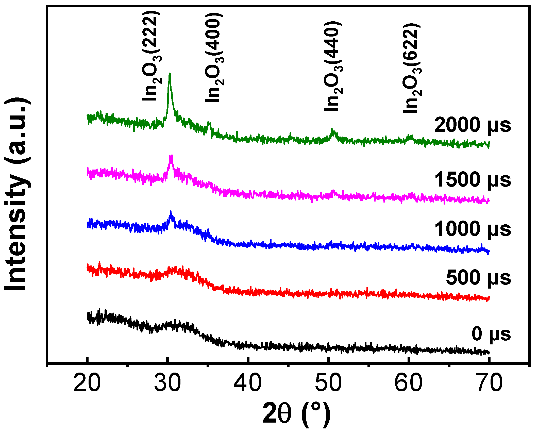
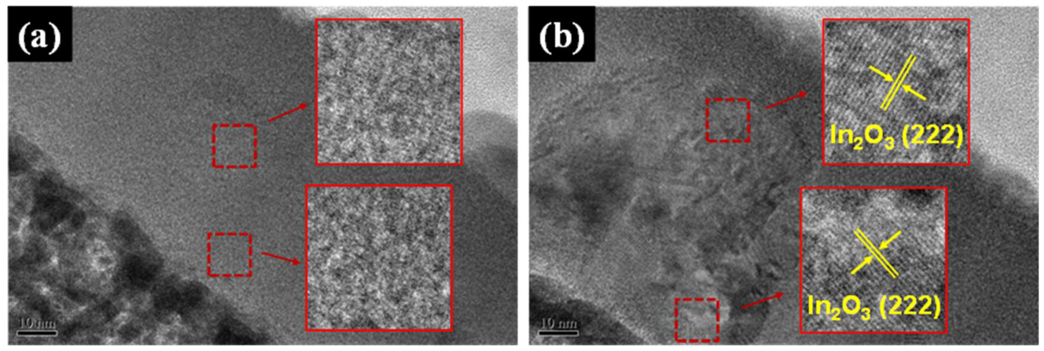
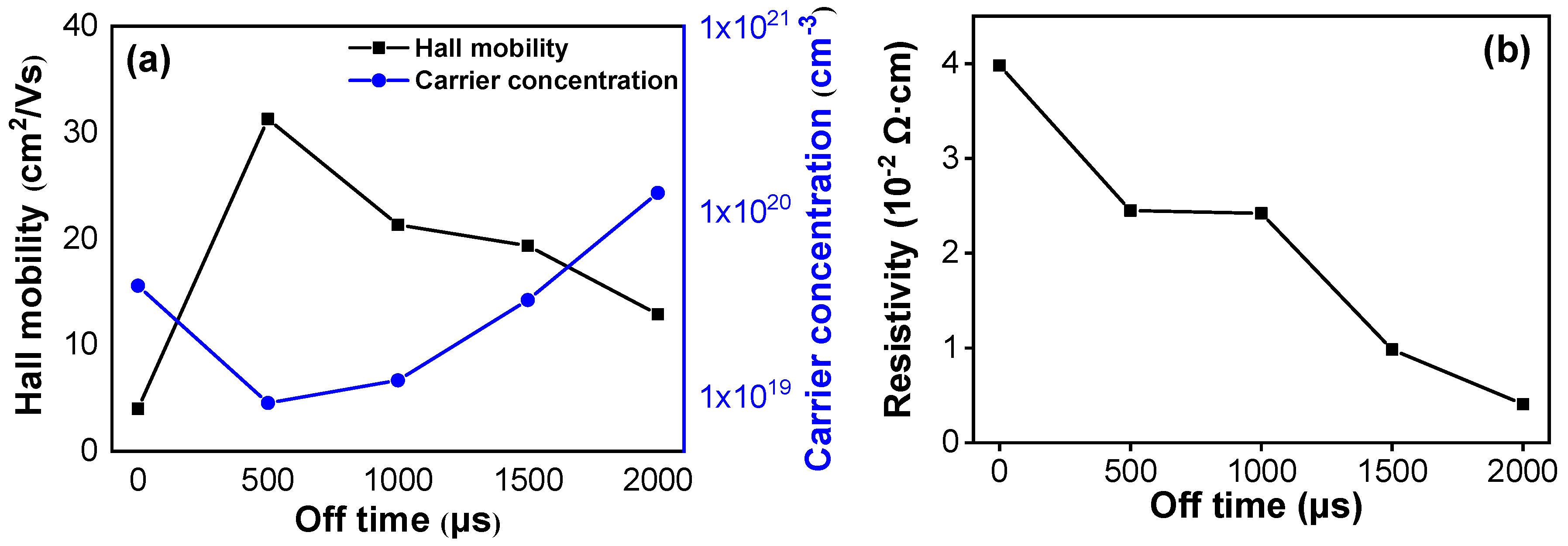
3. Results
4. Conclusions
Author Contributions
Funding
Acknowledgments
Conflicts of Interest
References
- Lee, C.C.; Wang, C.W. Interfacial fracture investigation of patterned active matrix OLED driven by amorphous-Si TFTs under film-type packaging technology. Appl. Surf. Sci. 2020, 510, 145428. [Google Scholar] [CrossRef]
- Hong, Y.; Wu, M.; Bae, J.H.; Hong, S.; Jeong, Y.; Jang, D.; Kim, J.S.; Hwang, C.S.; Park, B.-G.; Lee, J.H. A new sensing mechanism of Si FET-based gas sensor using pre-bias. Sens. Actuators B Chem. 2020, 302, 127147. [Google Scholar] [CrossRef]
- Song, J.H.; Kim, K.S.; Mo, Y.G.; Choi, R.; Jeong, J.K. Achieving High Field-Effect Mobility Exceeding 50 cm2/Vs in In-Zn-Sn-O Thin-Film Transistors. IEEE Electron Device Lett. 2014, 35, 853. [Google Scholar] [CrossRef]
- Sun, H.; Chen, S.C.; Peng, W.C.; Wen, C.K.; Wang, X.; Chuang, T.H. The influence of oxygen flow ratio on the optoelectronic properties of p-Type Ni1−xO films deposited by ion beam assisted sputtering. Coatings 2018, 8, 168. [Google Scholar] [CrossRef] [Green Version]
- Tiwari, B.; Bahubalindruni, P.G.; Santos, A.; Santa, A.; Figueiredo, C.; Pereira, M.; Martins, R.; Fortunato, E.; Barquinha, P. Low-Voltage High-Speed Ring Oscillator With a-InGaZnO TFTs. IEEE J. Electron Devices Soc. 2020, 8, 584–588. [Google Scholar] [CrossRef]
- Marrani, A.G.; Bonomo, M.; Dini, D. Adsorption Dynamics of Redox Active Species onto Polarized Surfaces of Sensitized NiO. ACS Omega 2019, 4, 1690–1699. [Google Scholar] [CrossRef]
- Kim, J.; Park, J.; Yoon, G.; Khushabu, A.; Kim, J.S.; Pae, S.; Cho, E.C.; Yi, J. Effect of IGZO thin films fabricated by Pulsed-DC and RF sputtering on TFT characteristics. Mater. Sci. Semicond. Process. 2020, 120, 105264. [Google Scholar] [CrossRef]
- Sun, H.; Jen, S.U.; Chiang, H.P.; Chen, S.C.; Lin, M.H.; Chen, J.Y.; Wang, X. Investigation of optoelectronic performance in In, Ga co-doped ZnO thin films with various In and Ga levels. Thin Solid Films 2017, 641, 12–18. [Google Scholar] [CrossRef]
- Chae, M.S.; Park, J.H.; Son, H.W.; Hwang, K.S.; Kim, T.G. IGZO-based electrolyte-gated field-effect transistor for in situ biological sensing platform. Sens. Actuators B Chem. 2018, 262, 876–883. [Google Scholar] [CrossRef]
- Jia, J.; Torigoshi, Y.; Shigesato, Y. In situ analyses on negative ions in the indium-gallium-zinc oxide sputtering process. Appl. Phys. Lett. 2013, 103, 013501. [Google Scholar] [CrossRef]
- Tomai, S.; Nishimura, M.; Itose, M.; Matuura, M.; Kasami, M.; Matsuzaki, S.; Kawashima, H.; Utsumo, F.; Uano, K. High-Performance Thin Film Transistor with Amorphous In2O3–SnO2–ZnO Channel Layer. Jpn. J. Appl. Phys. 2012, 51, 03CB01. [Google Scholar] [CrossRef]
- Jang, J.; Kim, D.G.; Kim, D.M.; Choi, S.J.; Lim, J.H.; Lee, J.H.; Kim, Y.S.; Ahn, B.D.; Kim, D.H. Investigation on the negative bias illumination stress-induced instability of amorphous indium-tin-zinc-oxide thin film transistors. Appl. Phys. Lett. 2014, 105, 152108. [Google Scholar] [CrossRef]
- Jia, J.; Torigoshi, Y.; Kawashima, E.; Utsuno, F.; Yano, K.; Shigesato, Y. Amorphous indium-tin-zinc oxide films deposited by magnetron sputtering with various reactive gases: Spatial distribution of thin film transistor performance. Appl. Phys. Lett. 2015, 106, 023502. [Google Scholar] [CrossRef]
- Noh, J.Y.; Kim, H.; Nahm, H.H.; Kim, Y.S.; Kim, D.H.; Ahn, B.D.; Lim, J.H.; Kim, G.H.; Lee, J.H.; Song, J. Cation composition effects on electronic structures of In-Sn-Zn-O amorphous semiconductors. J. Appl. Phys. 2013, 113, 183706. [Google Scholar] [CrossRef] [Green Version]
- Li, Z.Y.; Chen, S.C.; Huo, Q.H.; Liao, M.H.; Dai, M.J.; Lin, S.S.; Yang, T.L.; Sun, H. Influence of sputtering power on the electrical properties of In-Sn-Zn oxide thin films deposited by high power impulse magnetron sputtering. Coatings 2019, 9, 715. [Google Scholar] [CrossRef] [Green Version]
- Wen, L.; Sahu, B.B.; Kim, H.R.; Han, J.G. Study on the electrical, optical, structural, and morphological properties of highly transparent and conductive AZO thin films prepared near room temperature. Appl. Surf. Sci. 2019, 473, 649–656. [Google Scholar] [CrossRef]
- Ayaz, S.; Mishra, P.K.; Sharma, R.K.; Kamal, S.; Sen, S. Structural, Optoelectronic, and Electrochemical Properties of Zn1–x(Ga0.5Al0.5)xO Nanoparticles for Supercapacitor Applications. ACS Appl. Nano Mater. 2020, 3, 4562–4573. [Google Scholar] [CrossRef]
- Li, Z.Y.; Yang, H.Z.; Chen, S.C.; Lu, Y.B.; Xin, Y.Q.; Yang, T.L.; Sun, H. Impact of active layer thickness of nitrogen-doped In–Sn–Zn–O films on materials and thin film transistor performances. J. Phys. 2018, 51, 175101. [Google Scholar] [CrossRef]
- Cui, Y.; Li, C.J.; Li, J.; Xiong, L.Y.; Liu, S. Characterization of FeCeAlY thin film deposited by magnetron sputtering and its corrosion resistance under high-temperature water vapor environment. Surf. Technol. 2020, 49, 72–78. [Google Scholar]
- Song, S.; Sun, H.; Chen, S.C.; Dai, M.; Wang, K.; Zheng, X.; Lu, Y.B.; Yang, T.L.; Yue, Z.M. The adhesion strength and mechanical properties of SiC films deposited on SiAlON buffer layer by magnetron sputtering. Surf. Coat. Technol. 2019, 360, 116–120. [Google Scholar] [CrossRef]
- Fan, X.; Huai, X.; Wang, J.; Jing, L.C.; Wang, T.; Liu, J.; Geng, H.Z. Low surface roughness graphene oxide film reduced with aluminum film deposited by magnetron sputtering. Nanomaterials 2021, 11, 1428. [Google Scholar] [CrossRef] [PubMed]
- Chen, S.C.; Kuo, T.Y.; Lin, H.C.; Chen, R.Z.; Sun, H. Optoelectronic properties of p-type NiO films deposited by direct current magnetron sputtering versus high power impulse magnetron sputtering. Appl. Surf. Sci. 2020, 508, 145106. [Google Scholar] [CrossRef]
- Lin, S.S.; Gao, D.; Su, Y.F.; Xu, W.; Guo, C.Q.; Li, H.; Shi, Q.; Wei, C.B.; Dai, M.J.; Yang, J.C. Effect of bias voltage on structure and properties of DLC films deposited by high power pulse magnetron sputtering. Mater. Res. Appl. 2020, 14, 1–8. [Google Scholar]
- Sun, H.; Kuo, T.Y.; Chen, S.C.; Chen, Y.H.; Lin, H.C.; Yazdi, M.A.P.; Billard, A. Contribution of enhanced ionization to the optoelectronic properties of p-type NiO films deposited by high power impulse magnetron sputtering. J. Eur. Ceram. Soc. 2019, 39, 5285–5291. [Google Scholar] [CrossRef]
- Ghailane, A.; Larhlimi, H.; Tamraoui, Y.; Makha, M.; Busch, H.; Fischer, C.B.; Alami, J. The effect of magnetic field configuration on structural and mechanical properties of TiN coatings deposited by HiPIMS and dcMS. Surf. Coat. Technol. 2020, 404, 126572. [Google Scholar] [CrossRef]
- Chuang, T.H.; Wen, C.K.; Chen, S.C.; Liao, M.H.; Liu, F.; Sun, H. p-type semi-transparent conductive NiO films with high deposition rate produced by superimposed high power impulse magnetron sputtering. Ceram. Int. 2020, 46, 27695–27701. [Google Scholar] [CrossRef]
- Wang, Z.; Li, Q.; Yuan, Y.; Yang, L.; Zhang, H.; Liu, Z.; Ouyang, J.T.; Chen, Q. The semi-conductor of ZnO deposited in reactive HiPIMS. Appl. Surf. Sci. 2019, 494, 384–390. [Google Scholar] [CrossRef]
- Stranak, V.; Bogdanowicz, R.; Sezemsky, P.; Wulff, H.; Kruth, A.; Smietana, M.; Kratochvil, J.; Cada, M.; Hubicka, Z. Towards high quality ITO coatings: The impact of nitrogen admixture in HiPIMS discharges. Surf. Coat. Technol. 2018, 335, 126–133. [Google Scholar] [CrossRef]
- Jia, J.; Torigoshi, Y.; Suko, A.; Nakamura, S.I.; Kawashima, E.; Utsuno, F.; Shigesato, Y. Effect of nitrogen addition on the structural, electrical, and optical properties of In-Sn-Zn oxide thin films. Appl. Surf. Sci. 2017, 396, 897–901. [Google Scholar] [CrossRef]
- Chen, S.C.; Huang, S.Y.; Sakalley, S.; Paliwal, A.; Chen, Y.H.; Liao, M.H.; Sun, H.; Biring, S. Optoelectronic properties of Cu3N thin films deposited by reactive magnetron sputtering and its diode rectification characteristics. J. Alloys Compd. 2019, 789, 428–434. [Google Scholar] [CrossRef]


| Parameters | Value | Parameters | Value |
|---|---|---|---|
| Target | ITZO | Background pressure (Pa) | <7 10−4 |
| Substrate | Glass/silicon | Working pressure (Pa) | 0.7 |
| ton (µs) | 50 | Ar flow rate (sccm) | 20 |
| toff (µs) | 0 → 2000 | Deposition temp. (°C) | ambient |
| Power (W) | 300 | Film thickness (nm) | ~100 |
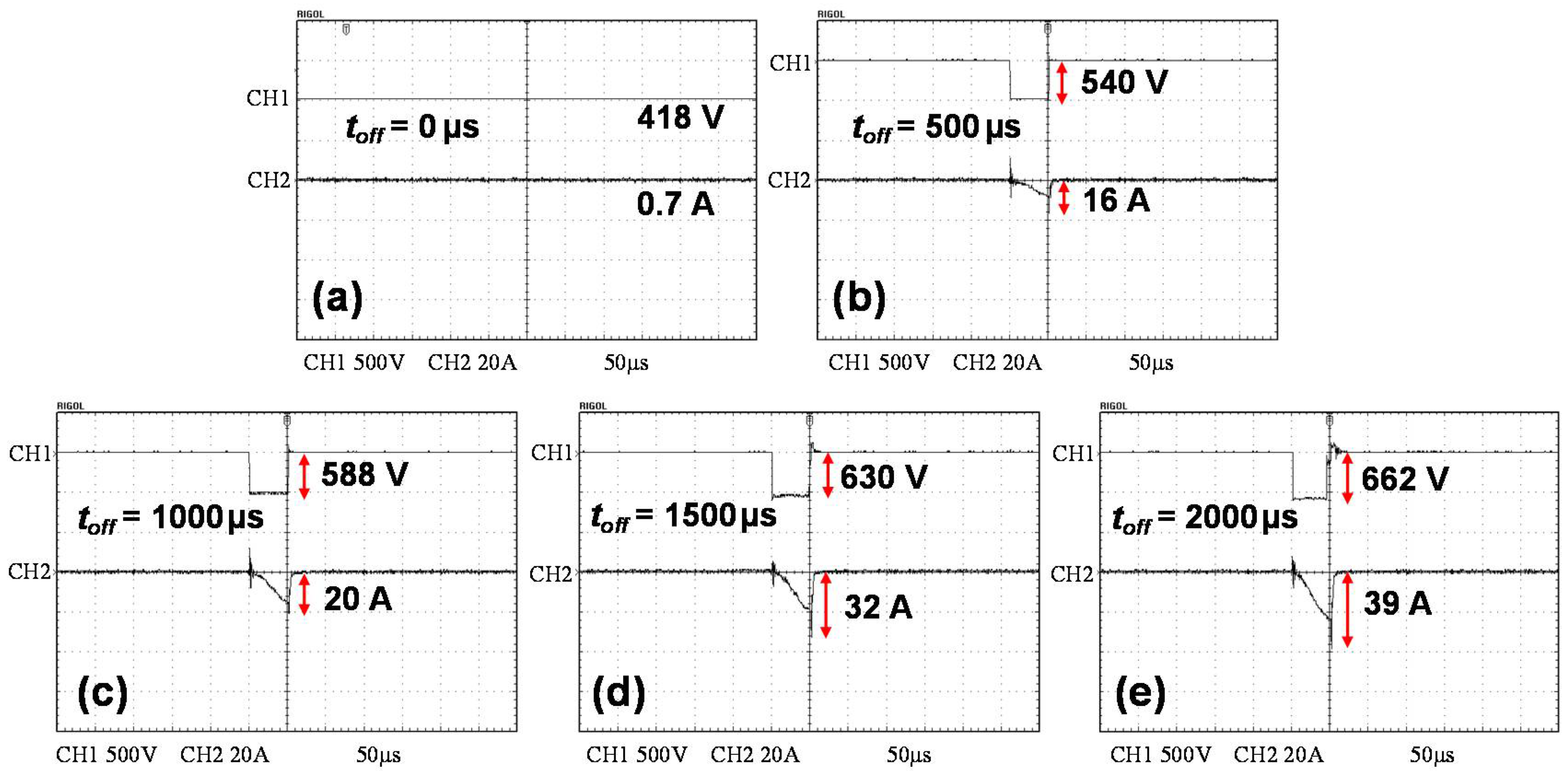
| toff (μs) | 0 | 500 | 1000 | 1500 | 2000 |
| Duty cycle (%) | 100 | 9.09 | 4.72 | 3.23 | 2.44 |
| Peak power density (W/cm2) | 6.42 | 189.47 | 257.89 | 442.11 | 531.97 |
| toff (μs) | In | Sn | Zn | O |
|---|---|---|---|---|
| 0 | 54.69 (±0.1) at.% | 3.49 (±0.1) at.% | 1.19 (±0.1) at.% | 40.63 (±0.1) at.% |
| 500 | 52.95 (±0.1) at.% | 3.47 (±0.1) at.% | 1.03 (±0.1) at.% | 42.56 (±0.1) at.% |
| 1000 | 52.31 (±0.1) at.% | 3.32 (±0.1) at.% | 1.19 (±0.1) at.% | 43.18 (±0.1) at.% |
| 1500 | 52.91 (±0.1) at.% | 3.56 (±0.1) at.% | 1.03 (±0.1) at.% | 42.50 (±0.1) at.% |
| 2000 | 51.67 (±0.1) at.% | 3.89 (±0.1) at.% | 1.14 (±0.1) at.% | 43.30 (±0.1) at.% |
Publisher’s Note: MDPI stays neutral with regard to jurisdictional claims in published maps and institutional affiliations. |
© 2021 by the authors. Licensee MDPI, Basel, Switzerland. This article is an open access article distributed under the terms and conditions of the Creative Commons Attribution (CC BY) license (https://creativecommons.org/licenses/by/4.0/).
Share and Cite
Sun, H.; Li, Z.-Y.; Chen, S.-C.; Liao, M.-H.; Gong, J.-H.; Bai, Z.; Wang, W.-X. In-Sn-Zn Oxide Nanocomposite Films with Enhanced Electrical Properties Deposited by High-Power Impulse Magnetron Sputtering. Nanomaterials 2021, 11, 2016. https://doi.org/10.3390/nano11082016
Sun H, Li Z-Y, Chen S-C, Liao M-H, Gong J-H, Bai Z, Wang W-X. In-Sn-Zn Oxide Nanocomposite Films with Enhanced Electrical Properties Deposited by High-Power Impulse Magnetron Sputtering. Nanomaterials. 2021; 11(8):2016. https://doi.org/10.3390/nano11082016
Chicago/Turabian StyleSun, Hui, Zhi-Yue Li, Sheng-Chi Chen, Ming-Han Liao, Jian-Hong Gong, Zhamatuofu Bai, and Wan-Xia Wang. 2021. "In-Sn-Zn Oxide Nanocomposite Films with Enhanced Electrical Properties Deposited by High-Power Impulse Magnetron Sputtering" Nanomaterials 11, no. 8: 2016. https://doi.org/10.3390/nano11082016
APA StyleSun, H., Li, Z.-Y., Chen, S.-C., Liao, M.-H., Gong, J.-H., Bai, Z., & Wang, W.-X. (2021). In-Sn-Zn Oxide Nanocomposite Films with Enhanced Electrical Properties Deposited by High-Power Impulse Magnetron Sputtering. Nanomaterials, 11(8), 2016. https://doi.org/10.3390/nano11082016