Article

Conformal Self-Assembly of Nanospheres for Light-Enhanced Airtightness Monitoring and Room-Temperature Gas Sensing

1
College of Advanced Interdisciplinary Studies, National University of Defense Technology, Changsha 410073, China
2
Beijing Institute for Advanced Study, National University of Defense Technology, Beijing 100000, China
3
State Key Laboratory of High Performance Computing, College of Computer Science and Technology, National University of Defense Technology, Changsha 410073, China
*
Authors to whom correspondence should be addressed.
Nanomaterials 2021, 11(7), 1829; https://doi.org/10.3390/nano11071829
Submission received: 22 June 2021 / Revised: 7 July 2021 / Accepted: 11 July 2021 / Published: 14 July 2021

Abstract

:
The fabrication of conformal nanostructures on microarchitectures is of great significance for diverse applications. Here a facile and universal method was developed for conformal self-assembly of nanospheres on various substrates including convex bumps and concave holes. Hydrophobic microarchitectures could be transferred into superhydrophilic ones using plasma treatment due to the formation of numerous hydroxyl groups. Because of superhydrophilicity, the nanosphere suspension spread on the microarchitectures quickly and conformal self-assembly of nanospheres can be realized. Besides, the feature size of the conformal nanospheres on the substrates could be further regulated by plasma treatment. After transferring two-dimensional tungsten disulfide sheets onto the conformal nanospheres, the periodic nanosphere array was demonstrated to be able to enhance the light harvesting of WS2. Based on this, a light-enhanced room-temperature gas sensor with a fast recovery speed (<35 s) and low detecting limit (500 ppb) was achieved. Moreover, the WS2-covered nanospheres on the microarchitectures were very sensitive to the changes in air pressure due to the formation of suspended sheets on the convex bumps and concave holes. A sensitive photoelectronic pressure sensor that was capable of detecting the airtightness of vacuum devices was developed using the WS2-decorated hierarchical architectures. This work provides a simple method for the fabrication of conformal nanospheres on arbitrary substrates, which is promising for three-dimensional microfabrication of multifunctional hierarchical microarchitectures for diverse applications, such as biomimetic compound eyes, smart wetting surfaces and photonic crystals.

1. Introduction

The utilization of conformal nanostructures formed on microarchitectures is of great significance for diverse applications, such as wetting tunability [1,2], flexible electronics [3,4], photodetectors [5], biomimetic photonics [6] and green energy [7]. Although micro/nanostructure fabrication via broad-range techniques of photolithography [8], laser etching [9], three-dimensional (3D) printing [10], thermal oxidation [11] and chemical deposition [12] has been highly developed, a method for validly constructing conformal nanostructures on complex microarchitectures remains elusive, especially for large-area fabrication of periodic nanostructures on convex and concave surfaces. With the merit of surface wrinkling, mechanical-driven assembly of wrinkling patterns has been demonstrated as an efficient method to fabricate nanostructures on curved substrates [13,14]. Tan et al. [15] obtained hierarchical wrinkled papillae arrays on spherical substrates via 3D shrinking-induced wrinkling of nonuniform graphene oxide films. Li et al. [14] fabricated multiscale microarchitecture arrays through photoinduced wrinkling of 3D microstructures. However, it is difficult to control the orientation and the feature size of wrinkling patterns on microarchitectures. Recently, the self-assembly of nanostructures (e.g., nanospheres, nanorods and nanowires) on microarchitectures has attracted much attention due to simple operation and high efficiency [16,17,18,19]. As a low-cost commercial nanomodule with tunable diameter, polystyrene (PS) nanospheres have been widely used in the fabrication of photonic crystals and sacrificial templates for antireflective microstructures [20], low-temperature gas sensors [21], photodetectors [22] and electromagnetic absorption [23]. However, most previous studies mainly focused on hexagonal stacking of PS nanospheres on flat substrates, while few studies concentrated on the assembly of nanospheres on curved microarchitectures, which may limit their applications in the fabrication of biomimetic compound eyes [24,25] and micro/nanorobots [26]. Therefore, it is crucial to develop a highly efficient assembly method for the formation of conformal nanostructures on various curved microarchitectures, especially for convex and concave surfaces.
Because of versatile functions and low cost, the fabrication of high-performance room-temperature gas sensors has become more and more important for environmental protection, gas leak detection and sustainable development [27,28,29]. Through the synthesis and design of micro/nanostructures, such as one-dimensional tubes [30], two-dimensional (2D) sheets [31] and 3D hierarchical architectures [32], many efforts have been put into improving the recoverability, stability and especially sensitivity and selectivity of the gas sensor [33,34,35,36]. For example, Yin et al. [37,38,39,40] prepared a series of gas sensors based on metal oxide nanoparticles and nanocomposites, and the sensors exhibited high sensitivity and selectivity in the detection of low-concentration H2 and CO gas. Due to tunable bandgap and high surface-to-volume ratio, 2D materials have been demonstrated as promising candidates for room-temperature gas sensing [41,42,43,44,45], also showing high potential in photoactivation recently [46,47,48,49]. As a member of the transition metal dichalcogenide (TMDC) family, tungsten disulfide (WS2) is applicable for the fabrication of light-enhanced room-temperature gas sensors due to broadband spectral response and fast relaxation interval [50,51,52,53,54]. Polyakov et al. [51] fabricated Au-decorated WS2 nanotubes for light-enhanced room-temperature detection of low-concentration NO2 gas using periodical 530 nm illumination. Huo et al. [52] constructed WS2-based field-effect transistors that can respond to both oxidizing gas and reducing gas at room temperature. Although the performance of WS2-based gas sensors can be improved using light illumination, the room-temperature gas sensor still suffers from a long recovery time and poor stability. The combination of hierarchical microarchitectures with the enhanced active area and photoresponsive 2D materials may shine some light on addressing this problem.
Herein, a facile, highly efficient and universal self-assembly method for the fabrication of conformal nanospheres on curved substrates including convex bumps and concave holes is proposed. The formation of nanosphere-supported WS2 sheets can be achieved by immersing the nanosphere-covered substrate into the WS2 suspension. Similar to the hierarchical papillae on the rose petals, the conformal nanosphere arrays were demonstrated to be able to enhance the interaction between the light and WS2 sheets. Besides, the WS2 sheets suspended over the nanospheres are very sensitive to the air pressure since the contact between the WS2 sheets and the nanospheres can be regulated by varying the pressure. These advantages make the nanosphere-supported WS2 sheets promising candidates for the fabrication of light-enhanced room-temperature gas sensors and sensitive pressure sensors. Impressively, a light-enhanced gas sensor with a fast recovery speed (<35 s) and a low detection limit (500 ppb NO2) is realized under room temperature based on the WS2-decorated nanospheres. In addition, an optoelectronic pressure sensor that is capable of monitoring the airtightness of vacuum devices is also fabricated by suspending the WS2 sheets over the nanosphere-covered microarchitectures. The pressure sensor exhibits a high sensitivity of 22.07 kPa−1 within the pressure range of 30 to 140 Pa. Particularly, the sensitivity of the light-enhanced pressure sensor increases dramatically with the reduction in air pressure from 101 to 0.03 kPa, enabling the pressure sensor to monitor the airtightness of vacuum devices. The fabrication method for suspended 2D WS2 sheets over 3D conformal nanospheres provides a new strategy for high-performance gas sensors and pressure detectors.

2. Materials and Methods

2.1. Polystyrene Nanospheres

The PS nanosphere suspension was purchased from Hangzhou Nano-Mall Technology Co., Ltd. (Hangzhou, China). The weight percentage of the PS nanospheres of the suspension is 2.5%, which can be diluted by the addition of deionized water. The average diameter of the nanospheres is 200 nm.

2.2. Flat and Curved Substrates

Smooth Pt electrodes and SiO2 substrates were selected as the substrates to investigate the assembly of PS nanospheres on flat metal and inorganic surfaces; they were provided by Beijing Sino Aggtech Co., Ltd. (Beijing, China). Bumpy Au electrodes and porous Polyethylene terephthalate (PET) substrates were selected as the curved substrates to study the assembly of PS nanospheres on convex and concave substrates, respectively.

2.3. Plasma Treatment of the Substrates

Before plasma treatment, the substrates were immersed in ethanol for 10 min and then dropped into an ultrasonic cleaner for 10 min. After that, the substrates were put into the chamber of plasma generator (PDC-36G) produced by Hefei Kejing Materials Technology Co., Ltd. (Hefei, China). The power was fixed at 18 W and the output frequency was 13.56 MHz.

2.4. Conformal Self-Assembly of the PS Nanospheres

After ultrasonic cleaning and plasma treatment, the hydrophobic substrates became superhydrophilic, which renders the suspension of PS nanospheres easy to spread around the surface, forming a uniform conformal coating of nanospheres. The substrates were immersed into the suspension of PS nanospheres for 5 min and then lifted out. Conformal nanosphere coatings can be obtained on various flat and curved substrates after solvent evaporation.

2.5. Fabrication of the WS2-Decorated Gas Sensor

Bumpy Au interdigital electrodes deposited on flexible porous PET substrates were used as the electrodes. Then, the PS nanospheres were conformally coated on the plasma-treated Au electrodes and PET substrates, forming hierarchical nanostructured surfaces. After that, the conformal nanosphere-coated surface was sputtered with a thin Au coating to improve the conductive network. Then, a plasma treatment of the Au-coated surfaces was carried out to enhance the adhesion between WS2 sheets and the nanostructured surfaces. Finally, WS2 suspension with a concentration of 1 mg/mL was directly dropped onto the conformal nanosphere-coated surfaces, leading to the formation of WS2-decorated nanosphere arrays with enhanced light-harvesting capability.

2.6. Characterization

Field emission scanning electron microscope MIRA 3 (TESCAN, Brno, Czech Republic) was used to characterize the surface morphology of various samples. Before characterization, the samples were sputtered with thin Au nanofilms to enhance their conductivity. The element analysis of WS2 sheets was carried out via the X-MAX20 (Oxford, UK) detector.

2.7. Performance of the Gas Sensor

The performance of the gas sensor was characterized with CGS-MT, an optoelectronics gas sensor test platform produced by Beijing Sino Aggtech Co., Ltd. (Beijing, China). A gas chamber with an optically polished quartz window was used to investigate the effect of light illumination on the performance of the gas sensor. The standard gas including NO2, CH2O, CO and NH3 was purchased from Shanghai Weichuang Standard Gas Analytical Technology Co., Ltd. (Shanghai, China). The test gas was calibrated according to the standard of GB/T5274-1-2018 (Gas analysis—Preparation of calibration gas mixtures—Part 1: Gravimetric method for Class I mixtures). The gravimetric method is an internationally recognized calibration method. The purchased standard gas was prepared by the gravimetric method. The test gas with various concentrations can be obtained by varying the concentration of the purchased standard gas using compressed dry air as carrier gas. Two mass flow controllers were used to mix different gases.

2.8. Performance of the Pressure Sensor

To characterize the performance of the pressure sensor, a vacuum pump (RV8) produced by Edwards was used to reduce the pressure of the chamber, and a vacuum gauge (ZJ-52T/kf10-16) produced by Chengdu Ruibao Electronic Technology Co., Ltd. (Chengdu, China) was used to measure the pressure of the test chamber. A semiconductor laser was used to produce high-quality light illumination of 532 nm wavelength.

3. Results and Discussion

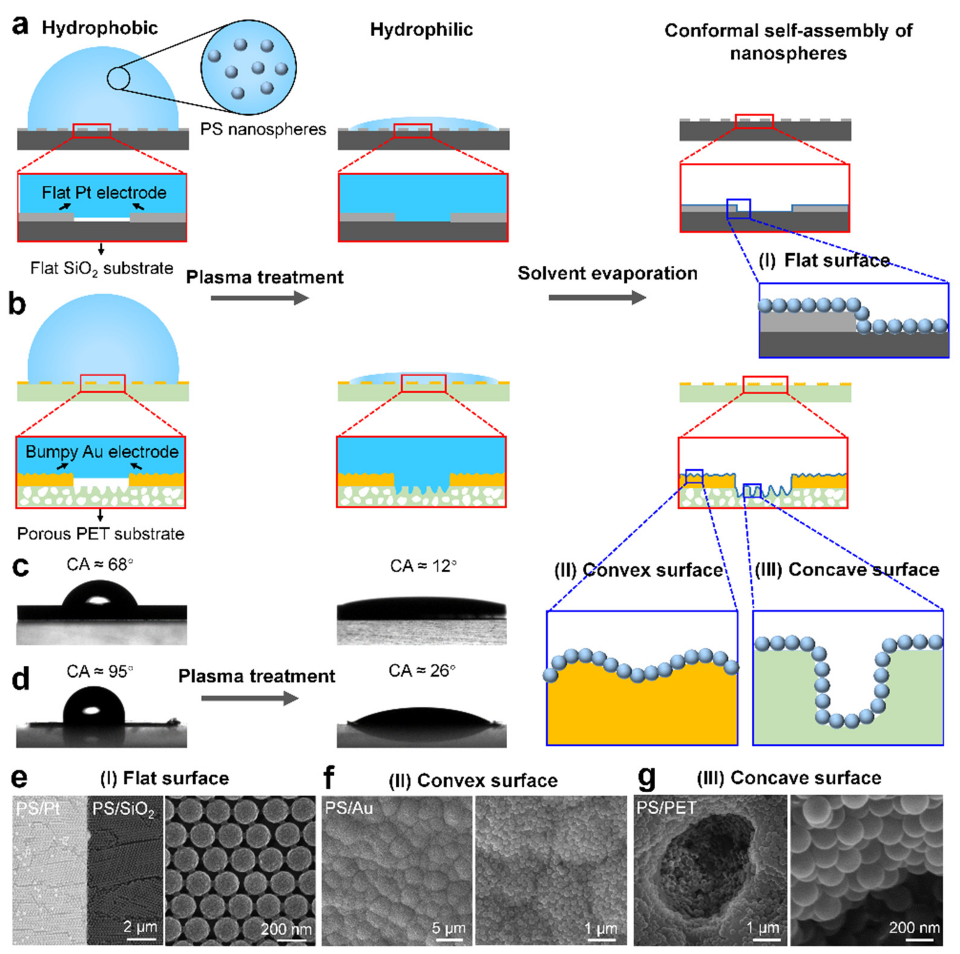
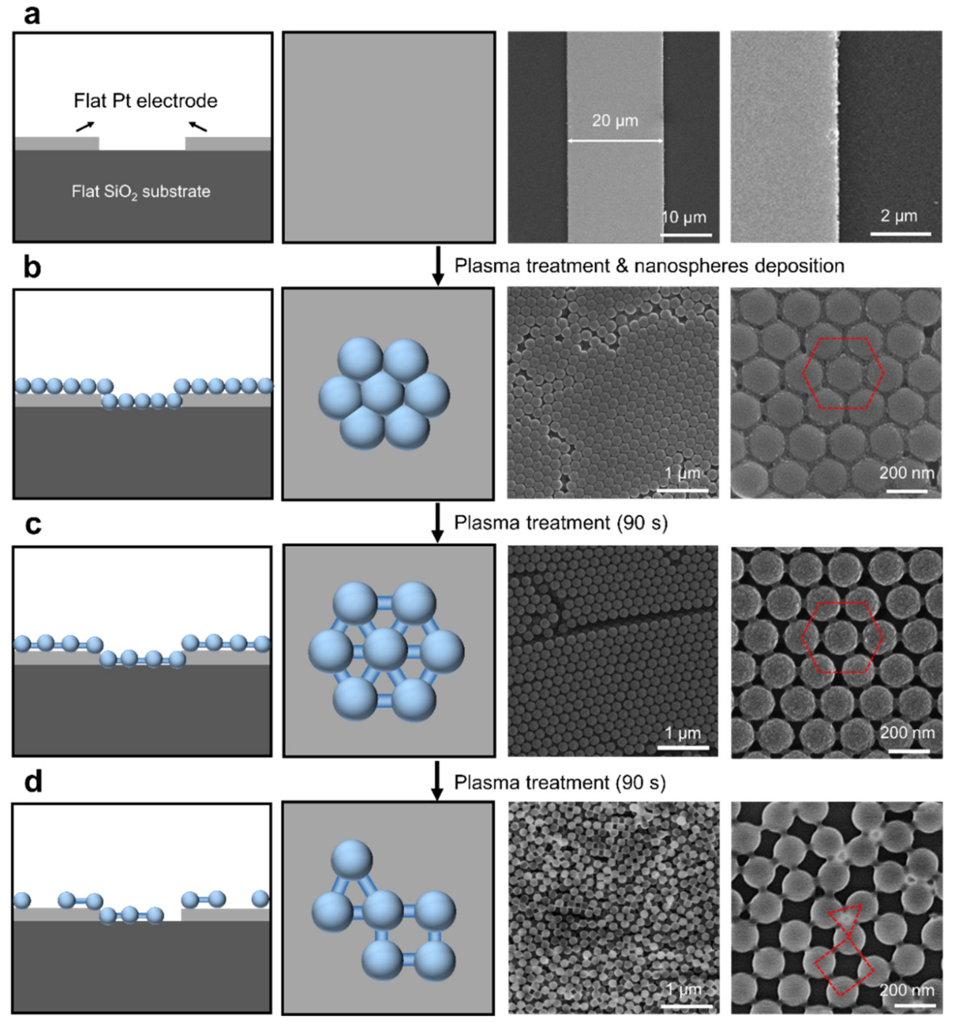
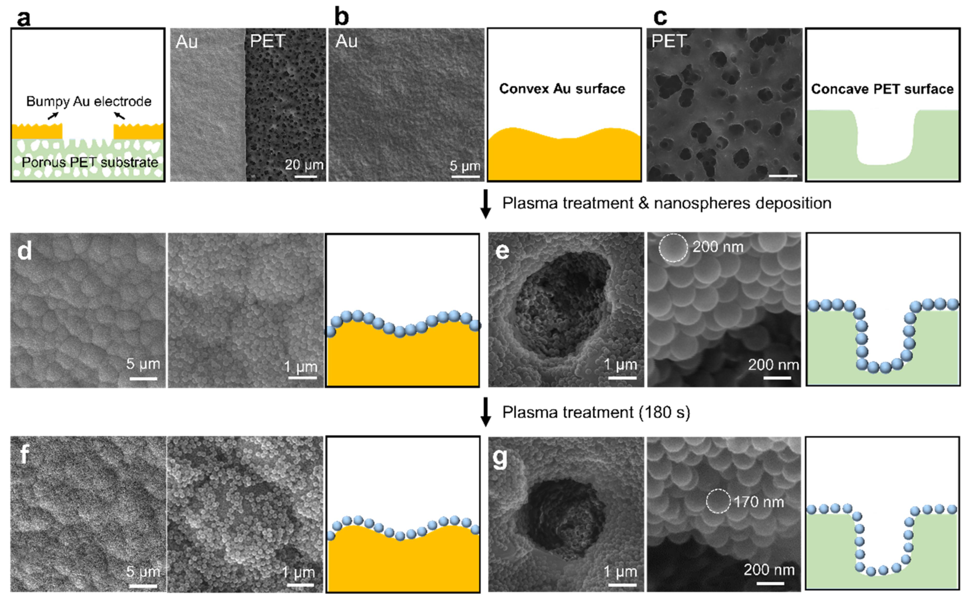
3.1. Conformal Assembly of Nanospheres on Flat and Curved Substrates

Figure 1a,b depicts the assembly process of conformal nanospheres on flat and curved substrates. Firstly, plasma treatment was used to enhance the hydrophilicity of the substrates, and the substrates became superhydrophilic due to the introduction of numerous hydrophilic hydroxyl groups (Figure 1c,d). For example, the contact angle of the hydrophobic Au-decorated PET substrate decreased from 95° to 26° after plasma treatment (Figure 1d). Then, the plasma-treated substrates were immersed into the suspension of PS nanospheres with an average diameter of 200 nm. Due to the superhydrophilicity of the substrates, the suspension containing nanospheres quickly spread onto the surfaces and penetrated the concave holes, forming uniform liquid films on the substrates. After solvent evaporation, conformal self-assembly of nanospheres can be realized on both flat and curved substrates. Importantly, the developed method for the self-assembly of conformal nanostructures on microarchitectures is suitable for various substrates that have different shapes and surface chemicals, such as flat metal and inorganic surfaces (Figure 1e), convex metal surfaces (Figure 1f) and concave polymer holes (Figure 1g). The plasma-enhanced adhesion between the substrates and the nanospheres not only prevents the nanospheres from slipping off the convex bumps but also promotes the self-assembly of nanospheres in the spatial-confinement holes.
The morphology evolution of the plasma-treated nanospheres on flat substrates was then characterized to see the effect of plasma treatment on the feature size and the arrangement of the self-assembled nanospheres (Figure 2). The SEM images in Figure 2a show that the surfaces of Pt and SiO2 substrates are flat. When the nanosphere suspension was spread onto the substrates, the nanospheres self-assembled into close-packed hexagonal arrays (Figure 2b). After a plasma treatment of 90 s, the close-packed nanospheres transferred into interconnected hexagonal skeletons consisting of balls and sticks (Figure 2c). Interestingly, the obtained ball–stick skeleton is very similar to the honeycomb molecular skeleton of graphene. With a further increase in the plasma treatment time, much more plasma etching was concentrated on the nanospheres, and the interconnected hexagonal skeletons evolved into randomly distributed nanospheres (Figure 2d). Besides, the diameter of the nanospheres decreased from 200 to 160 nm with the increase in the plasma treatment time from 0 to 180 s (Figure S1). The developed method for the self-assembly of nanospheres into ordered interconnected hexagonal skeletons provides a simple approach for constructing artificial molecular models for metastructures.
Although the assembly of nanospheres on flat substrates has been investigated intensively [55,56], the realization of a conformal assembly of nanospheres on convex bumps and concave holes is still challenging. With the use of the plasma treatment, the conformal assembly of nanospheres on curved substrates was next studied. As shown in Figure 3a–c, the undulating Au electrodes and the porous PET substrates were selected as the convex and concave surfaces to demonstrate the conformal assembly of nanospheres on curved substrates. As mentioned above, the substrates became superhydrophilic after plasma treatment. This makes it possible to realize the conformal assembly of nanospheres on bumps and holes. The nanosphere suspension spread quickly on the superhydrophilic substrates and the nanospheres were close-packed onto the substrates after solvent evaporation (Figure S2). It can be seen from the SEM images in Figure 3d,e that the nanospheres conformally covered on the Au microbumps and the PET microholes. Impressively, the nanospheres were close-packed on the inner surface of the microholes instead of filling up them, so the multilayer stacking of the nanospheres was avoided. Similarly, the diameter of the self-assembled nanospheres could be further reduced by additional plasma treatment. Particularly, the diameter of the nanospheres decreased from 200 to 170 nm after 180 s plasma treatment, as illustrated in Figure 3f,g (Figure S3). It is worth mentioning that the diameter of the nanospheres was reduced to 160 nm on a flat SiO2 substrate using the same treatment time. This indicates that the plasma etching is affected by the types of substrates, and flat substrates may be more beneficial for plasma etching. To clarify the morphology difference between thermal shrinking and plasma etching of PS nanospheres. The surface morphology of thermal-shrinking nanospheres was characterized (Figure S4). The conformal nanospheres on the bumpy Au electrodes and PET substrates were heated to 120 °C for 180 s. Different from the plasma-treated nanosphere array, the thermal-shrinking nanospheres agglomerated together, suggesting that plasma etching can better maintain the morphology of the nanospheres and avoid agglomeration.

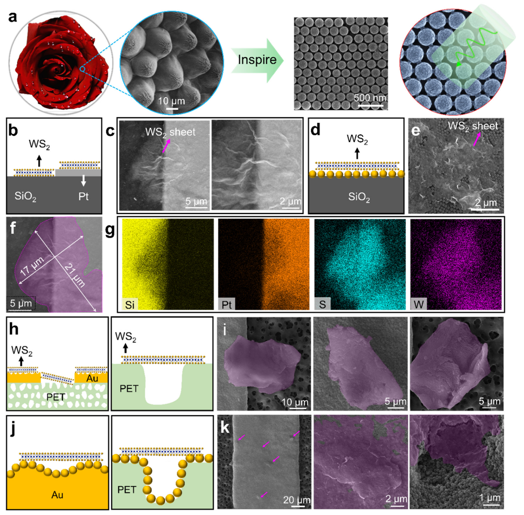
3.2. Decoration of WS2 Sheets on the Conformal Nanospheres

Many studies have demonstrated that the rose petal is capable of enhancing light harvesting due to periodic hierarchical papillae arrays on its surface [57,58], and a number of artificial papillary micro/nanostructures have been fabricated for improving the light-capturing efficiency of solar cells [59], as well as surface-enhanced Raman scattering [60,61]. Inspired by this, 2D WS2 sheets were loaded on the nanosphere array to enhance the interaction of light and WS2 (Figure 4a). The WS2 sheets were deposited onto the flat and the curved substrates by immersing the plasma-treated substrates into WS2 suspension with a concentration of 1 mg/mL. After solvent evaporation, the WS2 sheets with a feature size of ~20 μm spontaneously buckled into nanowrinkles on the substrates (Figure 4b,c). For the nanosphere-covered substrates, the WS2 sheets wrap the nanospheres and form undulating films (Figure 4d,e). The energy-dispersive spectroscopy (EDS) mapping and spectra further demonstrate that the WS2 sheets were successfully loaded on the flat Pt and SiO2 substrate (Figure 4f,g), as well as the nanosphere-covered substrates (Figure S5). Different from the flat substrates, the WS2 sheets tend to agglomerate on the surface of the bumpy Au electrode and the porous PET substrate, spontaneously folding into crumples (Figure 4h,i). Besides, the crumpled WS2 sheets overlap on the electrode and the substrate. By contrast, the WS2 sheets uniformly spread onto the nanosphere-coated curved substrates, forming continuous films on the nanosphere array (Figure 4j,k). Impressively, plenty of WS2 sheets suspend over the nanosphere-coated microholes, leading to the formation of numerous WS2-capsuled micro/nanocavities. These results suggest that the conformally coated nanospheres on the curved substrates are beneficial in facilitating the attachment of 2D materials.
The absorbance spectra of the WS2 sheets on the flat SiO2 substrate and the nanosphere-covered flat SiO2 substrate were characterized to see the effect of hexagonally packed nanospheres on the light absorbance. Two feature exciton absorption peaks of WS2 induced by two direct bandgap transitions were observed in the spectra: A exciton peak (~500–550 nm) and B exciton peak (~600–650 nm) (Figure S6) [62,63]. For simplicity, the nanosphere is abbreviated as NS, and the WS2-decorated nanospheres are abbreviated as WS2-NS. The light absorption of the WS2 sheet was demonstrated to be enhanced by suspending the WS2 sheet onto the nanosphere array, and a more than 15% increase in the absorbance of A and B exciton peaks was observed. This result shows that the interaction between WS2 sheets and the incident light can be effectively improved by introducing sub-wavelength nanosphere arrays.

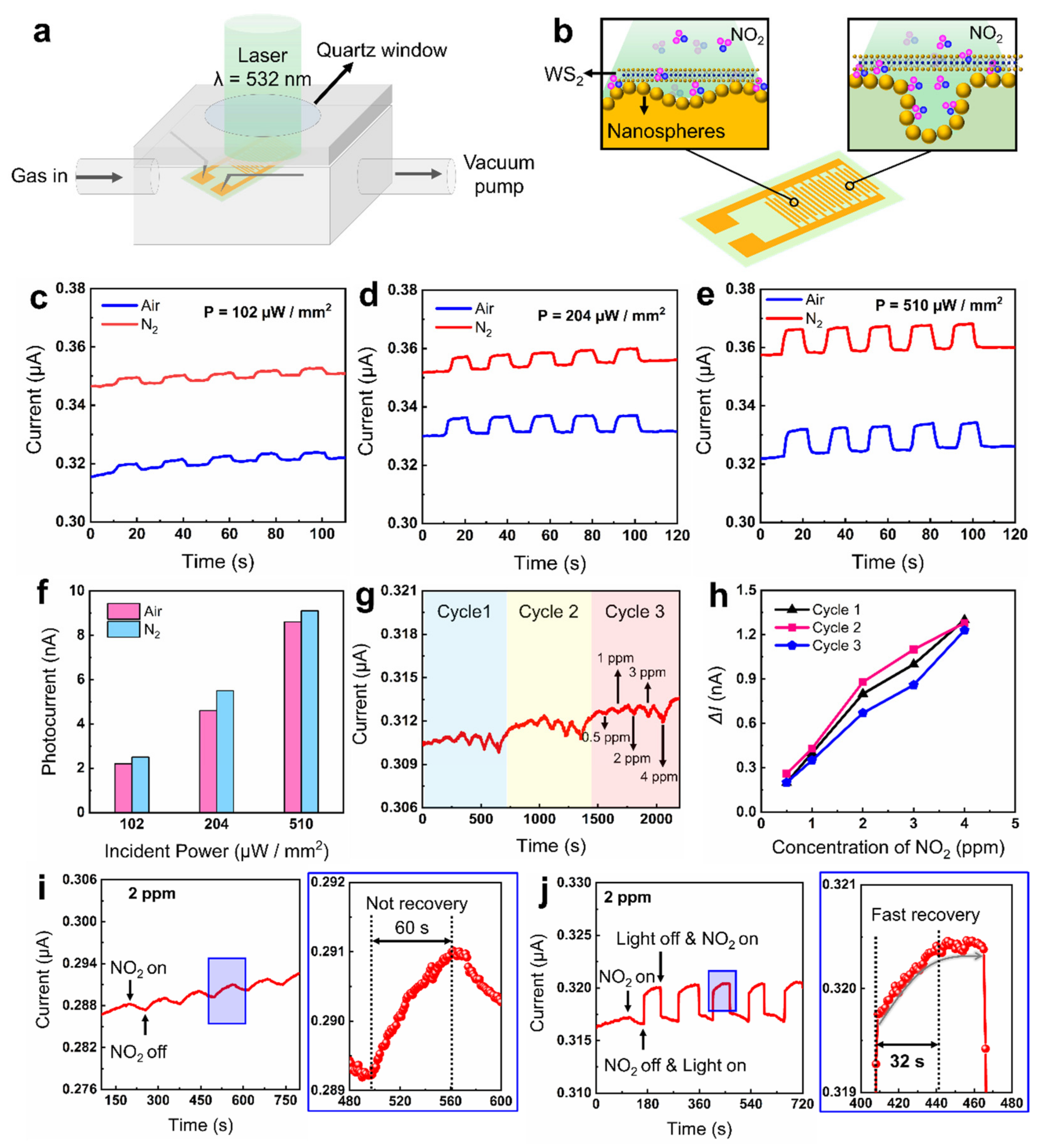
3.3. Light-Enhanced Room-Temperature Gas Sensing

With the advantages of photoresponsive 2D WS2 sheets and 3D nanosphere-coated microarchitectures, light-enhanced pressure monitors and gas sensors with excellent performance may be developed. WS2-decorated nanospheres (WS2-NS) on bumpy Au electrodes and porous PET substrates were fabricated to investigate their performance in airtightness monitoring and gas sensing (Figure 5a,b). A gas chamber equipped with a quartz window and metal probes was used to characterize the performance of the sensor (Figure 5a; Figure S7). It is worth mentioning that an Au nanofilm was sputtered on the nanospheres to improve the conductivity. Firstly, the photocurrent of the WS2-NS sensor in dry air and N2 gas was characterized to see the effect of O2 on the photoelectric property of the sensor. By increasing the incident power from 102 to 510 μW/mm2, the photocurrent increased from 2.2 to 8.6 nA in air (Figure 5c–e). After replacing the air with N2, the photocurrent increased slightly (Figure 5f). The air used in this work was dry air, and the main difference in the components between the dry air and the N2 is that the air contains O2 molecules. Compared with pure N2, the O2 molecules absorbed from the air can act as electron acceptors to induce a slight decrease in the current. This result is consistent with that of previous work [52]. Huo et al. [52] also demonstrated that the absorbed O2 molecules act as electron acceptors that are able to accept electrons from WS2, inducing a decrease in overall conductivity. Since the O2-induced decrease in the photocurrent was very small (less than 1 nA), the dry air could be used as the purge gas for the developed gas sensor.
As a typical toxic gas, the detection of low-concentration NO2 gas is of great significance for early warning of hazardous chemical exposure [46]. For example, the detection of NO2 exposure in a chemical warehouse may provide an early warning of spontaneous combustion and explosion so as to reduce economic losses. However, most room-temperature NO2 sensors suffer from slow recovery speed, which limits their application in timely warning of hazardous exposure. To speed up the recovery time, light illumination may be a simple and fast method. Considering low dark current and porous microstructures, the NO2 sensing performance of the WS2-NS sensor was investigated. Firstly, the response of the sensor under various gas concentrations without light illumination was characterized (Figure 5g). The current decrease (ΔI) induced by the NO2 within 60 s was used to characterize the response of the gas sensor. As shown in Figure 5h, the current response increased from 0.2 to 1.3 nA with the increase in the NO2 concentration from 0.5 to 4 ppm. Besides, the gas sensor exhibited good reproducibility and linearity through three absorption–desorption cycles. Then, the response of the gas sensor to 0.1, 0.2 and 0.5 ppm NO2 gas was measured to characterize the detection limit of the gas sensor (Supplementary Materials, Figure S8a). As a result, the detection limit of the gas sensor was demonstrated to be 0.5 ppm. Moreover, the sensor exhibited good selectivity in the detection of NO2 gas (Figure S8b). When various target gases, including CH2O, NH3, CO and NO2, with a concentration of 1 ppm were assessed, the sensor only showed an obvious response to the exposure of NO2 gas. However, it is still hard to realize the total desorption of the absorbed NO2 gas at room temperature. To clarify whether the light illumination is beneficial for NO2 desorption, the current response of the sensor to 2 ppm NO2 gas under dark and light illumination was studied (Figure 5i,j). The result shows that total desorption of NO2 was difficult to realize within 60 s. Impressively, the recovery time decreases remarkably to 32 s after introducing 532 nm light illumination during the gas desorption. This demonstrates that the photoexcited carriers are capable of reducing the recovery time of the NO2 gas sensor. Fast recovery speed makes the developed room-temperature gas sensor a promising candidate for monitoring hazardous exposure.

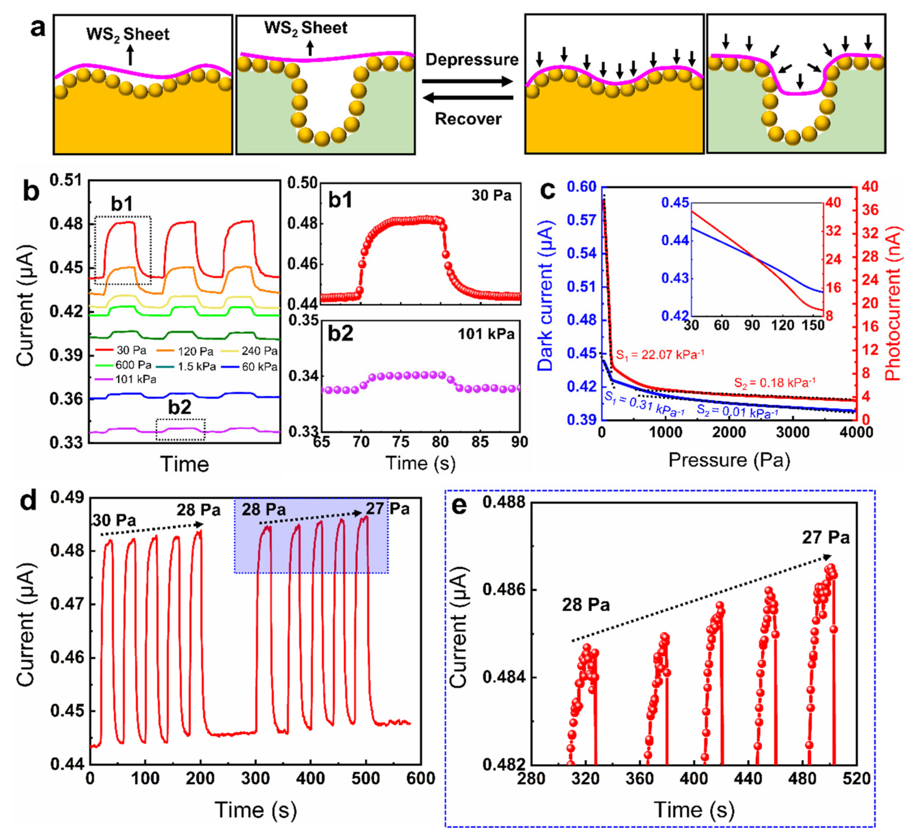
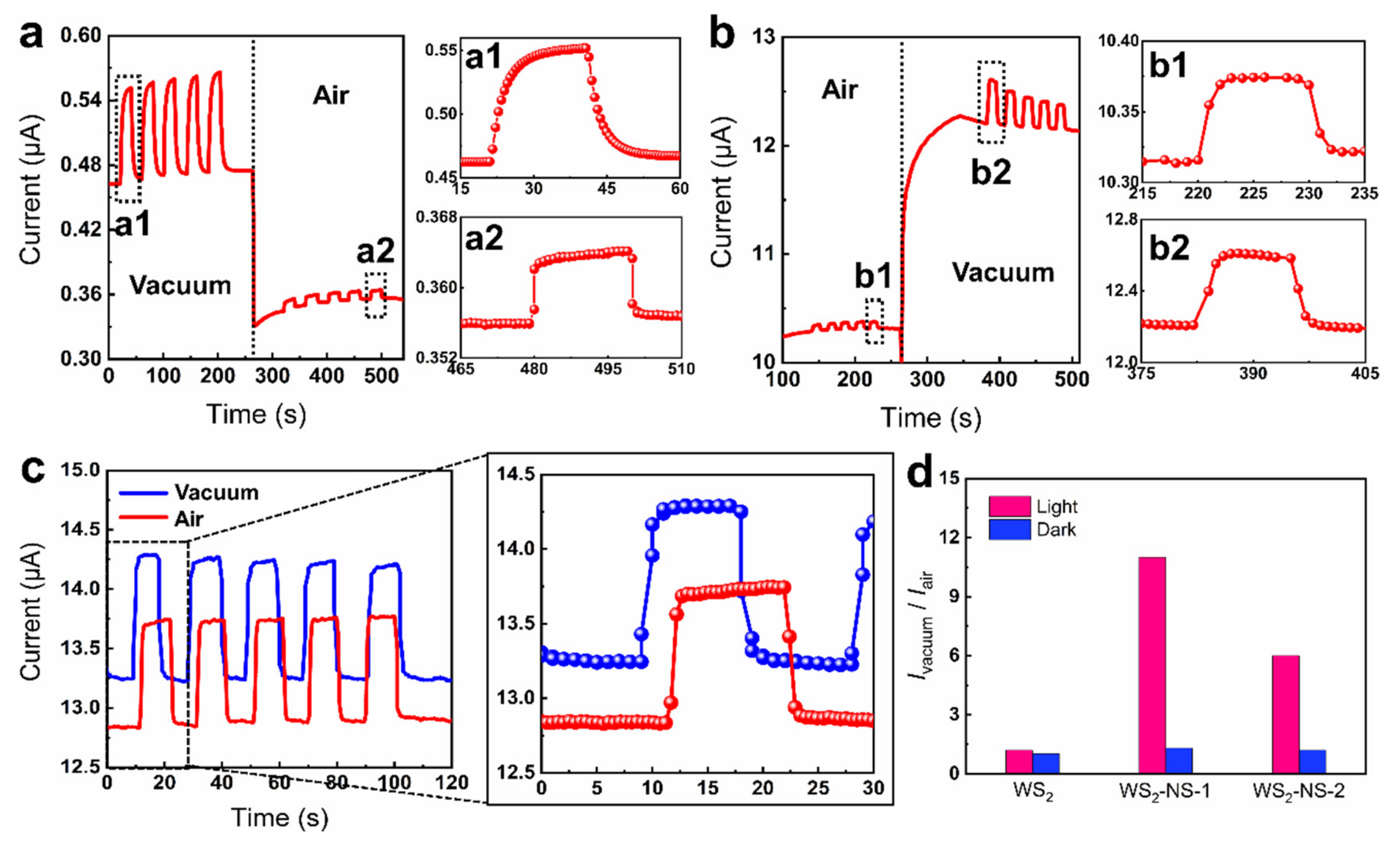
3.4. Light-Enhanced Airtightness Monitoring

The combination of 2D materials and conformal nanospheres on 3D microarchitectures provides a new avenue for designing gas sensors that are able to detect the gas pressure, which is crucial for gas detection under ultrahigh or ultralow ambient pressure. To address this challenge, photoenhanced pressure sensors based on the WS2-decorated nanospheres were designed (Figure 6a). For comparison, two types of sensors were fabricated: the WS2 sensor was obtained by directly depositing WS2 sheets on the interdigital electrode, and the WS2-NS sensor was achieved via coating the WS2 sheets onto the nanosphere-covered interdigital electrode. The photoresponse of the WS2-NS sensor under the pressure ranging from 0.03 to 101 kPa was characterized firstly (Figure 6b). Both the dark current and the photocurrent increased with the decrease in the air pressure (Figure 6c). For example, the photocurrent increased from 2.4 to 37.7 nA when the pressure was reduced from 101 to 0.03 kPa. Compared with the dark current, the photocurrent of the WS2-NS sensor is much more sensitive to pressure. The sensitivity (S) of the pressure sensor is defined as the ratio of the relative current change (ΔI/I0) to the pressure change (ΔP). A high sensitivity of 22.07 kPa−1 (~30–140 Pa) was demonstrated for the WS2-NS pressure sensor under light illumination, which is 71 times larger than that under dark conditions (~30–160 Pa). After that, the performance of the sensor responses to much lower pressure (e.g., 27 Pa) was characterized (Figure 6d). The results show that the sensor has excellent stability in the detection of pressure ranging from 0.027 to 101 kPa. Particularly, the sensitivity of the pressure sensor increased dramatically with the reduction in pressure below 200 Pa. For example, when the pressure is reduced from 30 to 27 Pa, the dark current and the photocurrent of the sensor increased by 4.1 and 1.3 nA, respectively (Figure S9). Currently, the lower and upper application limits of the WS2-NS sensor are 27 Pa and 101 kPa, respectively. In the future, we will continue to improve the test conditions and explore the performance of the sensor at much lower pressures (e.g., 10−4 Pa).
Because of high sensitivity to low pressure and fast response speed, the fabricated WS2-NS pressure sensor is suitable for airtightness monitoring. Two pressure sensors named WS2-NS-1 and WS2-NS-2 were fabricated by coating 1 and 2 mg/mL WS2 suspension onto the nanosphere-covered interdigital electrodes, so as to explore their performance in airtightness monitoring. Surprisingly, the photocurrent of the WS2/NS-1 sensor under vacuum (120 Pa) was 91 nA, 11 times higher than that in air (101 kPa) (Figure 7a). A fast and sharp decrease in the current was observed when the vacuum was broken by opening the air inlet. Accordingly, the photocurrent also decreased dramatically with the increase in pressure. This makes the WS2/NS sensor a promising candidate for monitoring airtightness in situations where a vacuum is needed. Compared with the WS2-NS-1 sensor, the WS2-NS-2 sensor exhibited a much higher dark current and photocurrent under both vacuum and air conditions (Figure 7b). Similarly, the WS2-NS-2 sensor was also demonstrated to be able to detect gas leakage in a dynamic-pressure environment.
By contrast, the current of the WS2 sensor without conformal nanospheres remained stable under both vacuum and air conditions (Figure 7c). The dark current of the sensor in air and under vacuum was as large as 12.8 and 13.2 μA, respectively, due to direct contact between the WS2 sheets and the electrode. Correspondingly, the photocurrents of the WS2 sensor were 0.87 μA in air and 1.04 μA under vacuum, respectively. The performance of the pressure sensor in airtightness monitoring was evaluated by the ratio of dark/photocurrent under vacuum (Ivacuum) to that in air (Iair). As shown in Figure 7d, the ratio of dark current under vacuum to that in air was lower than 1.5. Except for the WS2 sensor, both WS2-NS-1 and WS2-NS-2 sensors showed a vacuum-to-air photocurrent ratio higher than 6. This result further demonstrates the significance of conformal nanospheres in enhancing the sensitivity of the pressure sensor. For WS2-decorated conformal nanospheres on undulating substrates, numerous micro/nano air-pockets can be induced, and the contact between WS2 sheets and the nanospheres is poor in air. The contact area between the WS2 sheets and the nanospheres can be improved dramatically by depressuring, so as to induce a sharp decrease in the resistance. Similarly, depressure-induced better ohmic contact between the WS2 sheets and the substrates is also beneficial for the separation of electron–hole pairs, resulting in a much higher photocurrent. The combination of 2D materials and conformal nanospheres on curved surfaces provides a new avenue for the detection of airtightness, which may find applications in monitoring the airtightness of space aircraft.

4. Conclusions

In summary, a highly efficient self-assembly method was developed for the fabrication of conformal nanospheres on microarchitectures such as metal microbumps and polymer microholes. Plasma treatment plays a significant role in enhancing the hydrophilicity of the target substrates, and it is crucial for the conformal assembly of nanospheres. Different from previous methods, this approach is much more universal for fabricating conformal nanostructures on microarchitectures with various surface chemicals. Besides, plasma treatment was also demonstrated to be able to regulate the feature size of the conformal nanospheres. Similar to the hierarchical papillae array on the rose petal, the conformal nanospheres with nanogaps were demonstrated to be able to enhance the light harvesting of WS2 sheets. Based on this, a light-enhanced airtightness monitor and a room-temperature gas sensor with a fast recovery speed (<35 s) and low detecting limit (500 ppb) were developed. This work provides a universal method for fabricating conformal nanospheres on arbitrary substrates, especially for curved surfaces, which is promising for designing and fabricating artificial metasurfaces, biomimetic microarchitectures and other functional structures.

Supplementary Materials

The following are available online at https://www.mdpi.com/article/10.3390/nano11071829/s1, Figure S1: Controlling the feature size and the arrangement of the nanospheres on flat substrate by varying the plasma treatment time, Figure S2: Schematics illustrate the assembly mechanism of conformal nanospheres on flat and curved substrates, Figure S3: Controlling the feature size of the nanospheres on curved substrate by varying the plasma treatment time, Figure S4: Surface morphology of the PS nanospheres on curved substrates after thermal treatment, Figure S5: EDS analysis of the WS2 sheets loaded on the nanosphere array, Figure S6: Absorbance spectra of the WS2 sheets. Figure S7: Photographs show the mass flow controllers and the test chamber. Figure S8: Detection limit and selectivity of the gas sensor. Figure S9: Dark current and photocurrent of the sensor with the variation of the pressure.

Author Contributions

Conceptualization, Y.T. and T.J.; Methodology, Y.T.; Software, Q.L.; Validation, T.J., Y.T. and Q.L.; Formal Analysis, T.J., Y.K. and G.Z.; Investigation, Q.L. and Y.T.; Resources, Y.T.; Data Curation, Q.L.; Writing–Original Draft Preparation, Q.L. and Y.T.; Writing–Review & Editing, T.J. and R.Z.; Visualization, Y.T. and Q.L.; Supervision, Y.K. and X.Z.; Project Administration, T.J. and R.Z.; Funding Acquisition, T.J. and R.Z. All authors have read and agreed to the published version of the manuscript.

Funding

This research was funded by the Scientific Researches Foundation of National University of Defense Technology (ZK18-01-03); The Youth Talent Lifting Project (17-JCJQ-QT-004); National Natural Science Foundation of China (61801498).

Data Availability Statement

The data presented in this study are available on request from the corresponding author.

Conflicts of Interest

Authors declare no conflict of interest.

References

  1. Su, B.; Tian, Y.; Jiang, L. Bioinspired Interfaces with Superwettability: From Materials to Chemistry. J. Am. Chem. Soc. 2016, 138, 1727–1748. [Google Scholar] [CrossRef] [PubMed]
  2. Yan, X.; Huang, Z.; Sett, S.; Oh, J.; Cha, H.; Li, L.; Feng, L.; Wu, Y.; Zhao, C.; Orejon, D.; et al. Atmosphere-Mediated Superhydrophobicity of Rationally Designed Micro/Nanostructured Surfaces. ACS Nano 2019, 13, 4160–4173. [Google Scholar] [CrossRef] [Green Version]
  3. Rim, Y.S.; Bae, S.-H.; Chen, H.; Yang, J.L.; Kim, J.; Andrews, A.; Weiss, P.; Yang, Y.; Tseng, H.-R. Printable Ultrathin Metal Oxide Semiconductor-Based Conformal Biosensors. ACS Nano 2015, 9, 12174–12181. [Google Scholar] [CrossRef] [PubMed] [Green Version]
  4. Zhang, Z.; Li, H.; Miller, R.; Malissa, H.; Jamali, S.; Boehme, C.; Grossman, J.C.; Ren, S. Freestanding Organic Charge-Transfer Conformal Electronics. Nano Lett. 2018, 18, 4346–4354. [Google Scholar] [CrossRef] [PubMed]
  5. Yang, J.; Tang, L.; Luo, W.; Shen, J.; Zhou, D.; Feng, S.; Wei, X.; Shi, H. Light Trapping in Conformal Graphene/Silicon Nanoholes for High-Performance Photodetectors. ACS Appl. Mater. Interfaces 2019, 11, 30421–30429. [Google Scholar] [CrossRef]
  6. Kwon, Y.W.; Park, J.; Kim, T.; Kang, S.H.; Kim, H.; Shin, J.; Jeon, S.; Hong, S.W. Flexible Near-Field Nanopatterning with Ultrathin, Conformal Phase Masks on Nonplanar Substrates for Biomimetic Hierarchical Photonic Structures. ACS Nano 2016, 10, 4609–4617. [Google Scholar] [CrossRef]
  7. Ran, L.; Qiu, S.; Zhai, P.; Li, Z.; Gao, J.; Zhang, X.; Zhang, B.; Wang, C.; Sun, L.; Hou, J. Conformal Macroporous Inverse Opal Oxynitride-Based Photoanode for Robust Photoelectrochemical Water Splitting. J. Am. Chem. Soc. 2021, 143, 7402–7413. [Google Scholar] [CrossRef]
  8. Sun, J.; Litchinitser, N.M. Toward Practical, Subwavelength, Visible-Light Photolithography with Hyperlens. ACS Nano 2018, 12, 542–548. [Google Scholar] [CrossRef]
  9. Gilboa, T.; Zvuloni, E.; Zrehen, A.; Squires, A.H.; Meller, A. Automated, Ultra-Fast Laser-Drilling of Nanometer Scale Pores and Nanopore Arrays in Aqueous Solutions. Adv. Funct. Mater. 2020, 30, 1900642. [Google Scholar] [CrossRef]
  10. Zhou, L.; Fu, J.; He, Y. A Review of 3D Printing Technologies for Soft Polymer Materials. Adv. Funct. Mater. 2020, 30, 2000187. [Google Scholar] [CrossRef]
  11. Yin, X.-T.; Lv, P.; Li, J.; Jafari, A.; Wu, F.-Y.; Wang, Q.; Dastan, D.; Shi, Z.; Yu, S.; Garmestani, H. Nanostructured tungsten trioxide prepared at various growth temperatures for sensing applications. J. Alloys Compd. 2020, 825, 154105. [Google Scholar] [CrossRef]
  12. Jafari, A.; Alam, M.H.; Dastan, D.; Ziakhodadadian, S.; Shi, Z.; Garmestani, H.; Weidenbach, A.S.; Ţălu, Ş. Statistical, morphological, and corrosion behavior of PECVD derived cobalt oxide thin films. J. Mater. Sci. Mater. Electron. 2019, 30, 21185–21198. [Google Scholar] [CrossRef]
  13. Tan, Y.; Hu, B.; Song, J.; Chu, Z.; Wu, W. Bioinspired Multiscale Wrinkling Patterns on Curved Substrates: An Overview. Nano-Micro Lett. 2020, 12, 101. [Google Scholar] [CrossRef] [Green Version]
  14. Li, M.; Hakimi, N.; Perez, R.; Waldman, S.; Kozinski, J.A.; Hwang, D.K. Microarchitecture for a Three-Dimensional Wrinkled Surface Platform. Adv. Mater. 2015, 27, 1880–1886. [Google Scholar] [CrossRef]
  15. Tan, Y.; Hu, B.; Chu, Z.; Wu, W. Bioinspired Superhydrophobic Papillae with Tunable Adhesive Force and Ultralarge Liquid Capacity for Microdroplet Manipulation. Adv. Funct. Mater. 2019, 29, 1900266. [Google Scholar] [CrossRef]
  16. Liu, D.; Aleisa, R.; Cai, Z.; Li, Y.; Yin, Y. Self-assembly of superstructures at all scales. Matter 2021, 4, 927–941. [Google Scholar] [CrossRef]
  17. Yu, Y.; Ng, C.; König, T.A.F.; Fery, A. Tackling the Scalability Challenge in Plasmonics by Wrinkle-Assisted Colloidal Self-Assembly. Langmuir 2019, 35, 8629–8645. [Google Scholar] [CrossRef]
  18. Wang, Z.; Zhang, L.; Labib, M.; Chen, H.; Wei, M.; Poudineh, M.; Green, B.J.; Duong, B.; Das, J.; Ahmed, S.; et al. Peptide-functionalized nanostructured microarchitectures enable rapid mechanotransductive differentiation. ACS Appl. Mater. Interfaces 2019, 11, 41030–41037. [Google Scholar] [CrossRef]
  19. Brasse, Y.; Gupta, V.; Schollbach, H.C.T.; Karg, M.; König, T.A.F.; Fery, A. Mechanotunable Plasmonic Properties of Colloidal Assemblies. Adv. Mater. Interfaces 2020, 7, 1901678. [Google Scholar] [CrossRef] [Green Version]
  20. Yang, S.; Sun, N.; Stogin, B.B.; Wang, J.; Huang, Y.; Wong, T.-S. Ultra-antireflective synthetic brochosomes. Nat. Commun. 2017, 8, 1285. [Google Scholar] [CrossRef]
  21. Alenezy, E.K.; Sabri, Y.M.; Kandjani, A.E.; Korcoban, D.; Rashid, S.S.A.A.H.; Ippolito, S.J.; Bhargava, S.K. Low-Temperature Hydrogen Sensor: Enhanced Performance Enabled through Photoactive Pd-Decorated TiO2 Colloidal Crystals. ACS Sens. 2020, 5, 3902–3914. [Google Scholar] [CrossRef] [PubMed]
  22. Chen, Z.; Li, X.; Wang, J.; Tao, L.; Long, M.; Liang, S.-J.; Ang, L.K.; Shu, C.; Tsang, H.K.; Xu, J.-B. Synergistic Effects of Plasmonics and Electron Trapping in Graphene Short-Wave Infrared Photodetectors with Ultrahigh Responsivity. ACS Nano 2017, 11, 430–437. [Google Scholar] [CrossRef] [PubMed]
  23. Deng, Y.; Zheng, Y.; Zhang, D.; Han, C.; Cheng, A.; Shen, J.; Zeng, G.; Zhang, H. A novel and facile-to-synthesize three-dimensional honeycomb-like nano-Fe3O4@C composite: Electromagnetic wave absorption with wide bandwidth. Carbon 2020, 169, 118–128. [Google Scholar] [CrossRef]
  24. Shin, D.; Huang, T.; Neibloom, D.; Bevan, M.A.; Frechette, J. Multifunctional Liquid Marble Compound Lenses. ACS Appl. Mater. Interfaces 2019, 11, 34478–34486. [Google Scholar] [CrossRef] [PubMed]
  25. Wang, W.; Li, J.; Li, R.; Li, B.; Mei, X.; Sun, X. Fabrication of Hierarchical Micro/Nano Compound Eyes. ACS Appl. Mater. Interfaces 2019, 11, 34507–34516. [Google Scholar] [CrossRef] [PubMed]
  26. Zhou, H.; Mayorga-Martinez, C.C.; Pané, S.; Zhang, L.; Pumera, M. Magnetically Driven Micro and Nanorobots. Chem. Rev. 2021, 121, 4999–5041. [Google Scholar] [CrossRef] [PubMed]
  27. Xia, Y.; Zhou, L.; Yang, J.; Du, P.; Xu, L.; Wang, J. Highly Sensitive and Fast Optoelectronic Room-Temperature NO2 Gas Sensor Based on ZnO Nanorod-Assembled Macro-/Mesoporous Film. ACS Appl. Electron. Mater. 2020, 2, 580–589. [Google Scholar] [CrossRef]
  28. Kumar, R.; Goel, N.; Kumar, M. UV-Activated MoS2 Based Fast and Reversible NO2 Sensor at Room Temperature. ACS Sens. 2017, 2, 1744–1752. [Google Scholar] [CrossRef]
  29. Ko, K.Y.; Park, K.; Lee, S.; Kim, Y.; Woo, W.J.; Kim, D.; Song, J.-G.; Park, J. Recovery Improvement for Large-Area Tungsten Diselenide Gas Sensors. ACS Appl. Mater. Interfaces 2018, 10, 23910–23917. [Google Scholar] [CrossRef]
  30. Kwon, K.C.; Suh, J.M.; Lee, T.H.; Choi, K.S.; Hong, K.T.; Song, Y.G.; Shim, Y.-S.; Shokouhimehr, M.; Kang, C.-Y.; Kim, S.Y.; et al. SnS2 Nanograins on Porous SiO2 Nanorods Template for Highly Sensitive NO2 Sensor at Room Temperature with Excellent Recovery. ACS Sens. 2019, 4, 678–686. [Google Scholar] [CrossRef]
  31. Raghu, A.V.; Karuppanan, K.K.; Nampoothiri, J.; Pullithadathil, B. Wearable, Flexible Ethanol Gas Sensor Based on TiO2 Nanoparticles-Grafted 2D-Titanium Carbide Nanosheets. ACS Appl. Nano Mater. 2019, 2, 1152–1163. [Google Scholar] [CrossRef]
  32. Han, L.; Wang, D.; Lu, Y.; Jiang, T.; Liu, B.; Lin, Y. Visible-Light-Assisted HCHO Gas Sensing Based on Fe-Doped Flowerlike ZnO at Room Temperature. J. Phys. Chem. C 2011, 115, 22939–22944. [Google Scholar] [CrossRef]
  33. Nie, S.; Dastan, D.; Li, J.; Zhou, W.-D.; Wu, S.-S.; Zhou, Y.-W.; Yin, X.-T. Gas-sensing selectivity of n-ZnO/p-Co3O4 sensors for homogeneous reducing gas. J. Phys. Chem. Solids 2021, 150, 109864. [Google Scholar] [CrossRef]
  34. Yin, X.-T.; Dastan, D.; Wu, F.-Y.; Li, J. Facile Synthesis of SnO2/LaFeO3−XNX Composite: Photocatalytic Activity and Gas Sensing Performance. Nanomaterials 2019, 9, 1163. [Google Scholar] [CrossRef] [Green Version]
  35. Zhou, W.-D.; Dastan, D.; Yin, X.-T.; Nie, S.; Wu, S.; Wang, Q.; Li, J. Optimization of gas sensing properties of n-SnO2/p-xCuO sensors for homogenous gases and the sensing mechanism. J. Mater. Sci. Mater. Electron. 2020, 31, 18412–18426. [Google Scholar] [CrossRef]
  36. Zhou, W.-D.; Dastan, D.; Li, J.; Yin, X.-T.; Wang, Q. Discriminable Sensing Response Behavior to Homogeneous Gases Based on n-ZnO/p-NiO Composites. Nanomaterials 2020, 10, 785. [Google Scholar] [CrossRef] [Green Version]
  37. Yin, X.-T.; Wu, S.-S.; Dastan, D.; Nie, S.; Liu, Y.; Li, Z.-G.; Zhou, Y.-W.; Li, J.; Faik, A.; Shan, K.; et al. Sensing selectivity of SnO2-Mn3O4 nanocomposite sensors for the detection of H2 and CO gases. Surfaces Interfaces 2021, 25, 101190. [Google Scholar] [CrossRef]
  38. Yin, X.-T.; Li, J.; Dastan, D.; Zhou, W.-D.; Garmestani, H.; Alamgir, F.M. Ultra-high selectivity of H2 over CO with a p-n nanojunction based gas sensors and its mechanism. Sens. Actuators B Chem. 2020, 319, 128330. [Google Scholar] [CrossRef]
  39. Yin, X.-T.; Zhou, W.-D.; Li, J.; Wang, Q.; Wu, F.-Y.; Dastan, D.; Wang, D.; Garmestani, H.; Wang, X.-M.; Ţălu, Ş. A highly sensitivity and selectivity Pt-SnO2 nanoparticles for sensing applications at extremely low level hydrogen gas detection. J. Alloys Compd. 2019, 805, 229–236. [Google Scholar] [CrossRef]
  40. Yin, X.-T.; Zhou, W.-D.; Li, J.; Lv, P.; Wang, Q.; Wang, D.; Wu, F.-Y.; Dastan, D.; Garmestani, H.; Shi, Z.; et al. Tin dioxide nanoparticles with high sensitivity and selectivity for gas sensors at sub-ppm level of hydrogen gas detection. J. Mater. Sci. Mater. Electron. 2019, 30, 14687–14694. [Google Scholar] [CrossRef]
  41. Zhang, L.; Li, Z.; Liu, J.; Peng, Z.; Zhou, J.; Zhang, H.; Li, Y. Optoelectronic Gas Sensor Based on Few-Layered InSe Nanosheets for NO2 Detection with Ultrahigh Antihumidity Ability. Anal. Chem. 2020, 92, 11277–11287. [Google Scholar] [CrossRef] [PubMed]
  42. Zheng, W.; Xu, Y.; Zheng, L.; Yang, C.; Pinna, N.; Liu, X.; Zhang, J. MoS2 Van der Waals p–n Junctions Enabling Highly Selective Room-Temperature NO2 Sensor. Adv. Funct. Mater. 2020, 30, 2000435. [Google Scholar] [CrossRef]
  43. Kim, S.J.; Koh, H.-J.; Ren, C.E.; Kwon, O.; Maleski, K.; Cho, S.; Anasori, B.; Kim, C.-K.; Choi, Y.-K.; Kim, J.; et al. Metallic Ti3C2Tx MXene Gas Sensors with Ultrahigh Signal-to-Noise Ratio. ACS Nano 2018, 12, 986–993. [Google Scholar] [CrossRef] [PubMed] [Green Version]
  44. Cui, H.; Zheng, K.; Xie, Z.; Yu, J.; Zhu, X.; Ren, H.; Wang, Z.; Zhang, F.; Li, X.; Tao, L.-Q.; et al. Tellurene Nanoflake-Based NO2 Sensors with Superior Sensitivity and a Sub-Parts-per-Billion Detection Limit. ACS Appl. Mater. Interfaces 2020, 12, 47704–47713. [Google Scholar] [CrossRef] [PubMed]
  45. Guo, J.; Wen, R.; Zhai, J.; Wang, Z.L. Enhanced NO2 gas sensing of a single-layer MoS2 by photogating and piezo-phototronic effects. Sci. Bull. 2019, 64, 128–135. [Google Scholar] [CrossRef] [Green Version]
  46. Kumar, R.; Liu, X.; Zhang, J.; Kumar, M. Room-Temperature Gas Sensors Under Photoactivation: From Metal Oxides to 2D Materials. Nano-Micro Lett. 2020, 12, 164. [Google Scholar] [CrossRef]
  47. Yan, X.; Wu, Y.; Li, R.; Shi, C.; Moro, R.; Ma, Y.; Ma, L. High-Performance UV-Assisted NO2 Sensor Based on Chemical Vapor Deposition Graphene at Room Temperature. ACS Omega 2019, 4, 14179–14187. [Google Scholar] [CrossRef] [Green Version]
  48. Wu, E.; Xie, Y.; Yuan, B.; Zhang, H.; Hu, X.; Liu, J.; Zhang, D. Ultrasensitive and Fully Reversible NO2 Gas Sensing Based on p-Type MoTe2 under Ultraviolet Illumination. ACS Sens. 2018, 3, 1719–1726. [Google Scholar] [CrossRef]
  49. Mai, H.D.; Jeong, S.; Nguyen, T.K.; Youn, J.-S.; Ahn, S.; Park, C.-M.; Jeon, K.-J. Pd Nanocluster/Monolayer MoS2 Heterojunctions for Light-Induced Room-Temperature Hydrogen Sensing. ACS Appl. Mater. Interfaces 2021, 13, 14644–14652. [Google Scholar] [CrossRef]
  50. Ding, J.; Feng, A.; Li, X.; Ding, S.; Liu, L.; Ren, W. Properties, preparation, and application of tungsten disulfide: A review. J. Phys. D Appl. Phys. 2021, 54, 173002. [Google Scholar] [CrossRef]
  51. Polyakov, A.Y.; Kozlov, D.A.; Lebedev, V.A.; Chumakov, R.G.; Frolov, A.; Yashina, L.V.; Rumyantseva, M.N.; Goodilin, E. Gold Decoration and Photoresistive Response to Nitrogen Dioxide of WS2 Nanotubes. Chem. A Eur. J. 2018, 24, 18952–18962. [Google Scholar] [CrossRef]
  52. Huo, N.; Yang, S.; Wei, Z.; Li, S.-S.; Xia, J.-B.; Li, J. Photoresponsive and Gas Sensing Field-Effect Transistors based on Multilayer WS2 Nanoflakes. Sci. Rep. 2015, 4, 5209. [Google Scholar] [CrossRef] [Green Version]
  53. Paolucci, V.; Emamjomeh, S.M.; Ottaviano, L.; Cantalini, C. Near Room Temperature Light-Activated WS2-Decorated rGO as NO2 Gas Sensor. Sensors 2019, 19, 2617. [Google Scholar] [CrossRef] [Green Version]
  54. Gu, D.; Li, X.; Wang, H.; Li, M.; Xi, Y.; Chen, Y.; Wang, J.; Rumyntseva, M.N.; Gaskov, A.M. Light enhanced VOCs sensing of WS2 microflakes based chemiresistive sensors powered by triboelectronic nangenerators. Sens. Actuators B Chem. 2018, 256, 992–1000. [Google Scholar] [CrossRef]
  55. Banik, M.; Mukherjee, R. Fabrication of Ordered 2D Colloidal Crystals on Flat and Patterned Substrates by Spin Coating. ACS Omega 2018, 3, 13422–13432. [Google Scholar] [CrossRef]
  56. Jeon, H.; Kim, D.J.; Park, M.S.; Ryu, D.Y.; Kim, J.H. Amphiphilic Graft Copolymer Nanospheres: From Colloidal Self-Assembly to CO2 Capture Membranes. ACS Appl. Mater. Interfaces 2016, 8, 9454–9461. [Google Scholar] [CrossRef]
  57. Feng, L.; Zhang, Y.; Li, M.; Zheng, Y.; Shen, W.; Jiang, L. The Structural Color of Red Rose Petals and Their Duplicates. Langmuir 2010, 26, 14885–14888. [Google Scholar] [CrossRef]
  58. Chen, A.; Qian, J.; Chen, Y.; Lu, X.; Wang, F.; Tang, Z. Enhanced sunlight photocatalytic activity of porous TiO2 hierarchical nanosheets derived from petal template. Powder Technol. 2013, 249, 71–76. [Google Scholar] [CrossRef]
  59. Hünig, R.; Mertens, A.; Stephan, M.; Schulz, A.; Richter, B.; Hetterich, M.; Powalla, M.; Lemmer, U.; Colsmann, A.; Gomard, G. Flower Power: Exploiting Plants’ Epidermal Structures for Enhanced Light Harvesting in Thin-Film Solar Cells. Adv. Opt. Mater. 2016, 4, 1487–1493. [Google Scholar] [CrossRef]
  60. Chou, S.-Y.; Yu, C.-C.; Yen, Y.-T.; Lin, K.-T.; Chen, H.-L.; Su, W.-F. Romantic Story or Raman Scattering? Rose Petals as Ecofriendly, Low-Cost Substrates for Ultrasensitive Surface-Enhanced Raman Scattering. Anal. Chem. 2015, 87, 6017–6024. [Google Scholar] [CrossRef]
  61. Xu, B.-B.; Zhang, Y.-L.; Zhang, W.-Y.; Liu, X.-Q.; Wang, J.-N.; Zhang, X.-L.; Zhang, D.-D.; Jiang, H.; Zhang, R.; Sun, H.-B. Silver-Coated Rose Petal: Green, Facile, Low-Cost and Sustainable Fabrication of a SERS Substrate with Unique Superhydrophobicity and High Efficiency. Adv. Opt. Mater. 2013, 1, 56–60. [Google Scholar] [CrossRef]
  62. Zhao, W.; Ghorannevis, Z.; Chu, L.; Toh, M.; Kloc, C.; Tan, P.-H.; Eda, G. Evolution of Electronic Structure in Atomically Thin Sheets of WS2 and WSe2. ACS Nano 2013, 7, 791–797. [Google Scholar] [CrossRef] [Green Version]
  63. Ramasubramaniam, A. Large excitonic effects in monolayers of molybdenum and tungsten dichalcogenides. Phys. Rev. B 2012, 86, 115409. [Google Scholar] [CrossRef] [Green Version]
Figure 1. Conformal self-assembly of nanospheres on flat and curved substrates. (a,b) Schematics illustrate the fabrication process for conformal nanospheres on (a) flat and (b) curved substrates. (c,d) Improving the hydrophilicity of the substrates by plasma treatment: (c) Pt electrodes on SiO2 substrates; (d) Au electrodes on polyethylene terephthalate (PET) substrate. (eg) SEM images show the conformal nanospheres on (e) flat Pt and SiO2 substrate, (f) convex Au substrate and (g) concave PET substrate.
Nanomaterials 11 01829 g001
Figure 2. Controlling the feature size and the arrangement of the nanospheres on flat substrates via plasma treatment. (ad) Schematics and SEM images show the morphology of (a) the flat Pt and SiO2 substrate, as well as the morphology evolution of the self-assembled nanospheres on the substrates with the variation of the plasma treatment time: (b) 0 s, (c) 90 s and (d) 180 s.
Nanomaterials 11 01829 g002
Figure 3. Conformal self-assembly of nanospheres on convex and concave substrates. (ac) Schematics and SEM images of the substrates: (a) bumpy Au electrodes on porous PET substrate; (b) the undulating Au substrate; (c) the concave PET substrate. (dg) SEM images and the schematics show the morphology of the nanosphere assembly on curved substrates (d,e) before and (f,g) after plasma treatment.
Nanomaterials 11 01829 g003
Figure 4. The fabrication of 2D WS2 sheets on rose-petal-inspired nanosphere array. (a) Biomimetic strategy for enhancing light harvesting using the nanosphere array; the photo and SEM image of rose petal were taken by the author. (be) Schematics and SEM images show WS2-decorated (b,c) flat substrates and (d,e) nanosphere-covered substrate. (f,g) SEM image and EDS mapping results of the WS2-decorated Pt and SiO2 substrates. (hk) Schematics and SEM images show the WS2-decorated (h,i) Au and PET substrate and (j,k) conformal nanosphere-coated substrates. The WS2 sheets in the SEM images are highlighted with purple color.
Nanomaterials 11 01829 g004
Figure 5. WS2-decorated nanospheres for light-enhanced room-temperature gas sensing. (a,b) Schematics of (a) the test platform and (b) the WS2-decorated nanospheres (WS2-NS) on the interdigital electrode for NO2 sensing. (ce) Photoresponse of the WS2-NS sensor to air and N2 under various incident power conditions: (c) 102 µW/mm2, (d) 204 µW/mm2, (e) 510 µW/mm2. (f) Photocurrent of the sensor with the variation of the incident power. (g,h) Current changes with the variation of NO2 concentration from 0.5 to 4 ppm under room temperature (26 °C). (i) Cycling response of the gas sensor to 2 ppm NO2 gas. (j) Light-enhanced gas desorption. The incident power is 102 µW/mm2.
Nanomaterials 11 01829 g005
Figure 6. WS2-decorated nanospheres for photoresponsive pressure sensor. (a) Schematics illustrate the sensing mechanism of the WS2-NS pressure sensor. (b) Photoresponse of the WS2-NS sensor under various pressure conditions: (b1) 30 Pa; (b2) 101 kPa. (c) Dark current and photocurrent of the sensor with the variation of the pressure. (d) Photoresponse of the WS2-NS sensor a decrease in pressure from 30 to 27 Pa. (e) Enlarged view of the blue box in Figure 6d. The incident power is 102 µW/mm2.
Nanomaterials 11 01829 g006
Figure 7. Demonstration of the WS2-NS pressure sensor for airtightness monitoring. (a,b) Controlling the photoresponse of the WS2-NS sensor under vacuum and air conditions by varying the concentration of WS2 suspension: (a) 1 mg/mL; (b) 2 mg/mL. The obtained sensors are named WS2-NS-1 and WS2-NS-2, respectively. (c) Dynamic response of the WS2 sensor without nanosphere coatings. The incident power is 510 µW/mm2. (d) The ratio of the dark/photocurrent in vacuum to that in air.
Nanomaterials 11 01829 g007
Publisher’s Note: MDPI stays neutral with regard to jurisdictional claims in published maps and institutional affiliations.

