
Formation Mechanisms and Phase Stability of Solid-State Grown CsPbI3 Perovskites

 ,
,  ,
,  ,
,  , and
, and 
Abstract
:
1. Introduction
2. Material and Methods
2.1. Materials
2.2. Synthesis
2.3. Characterization
3. Results and Discussion
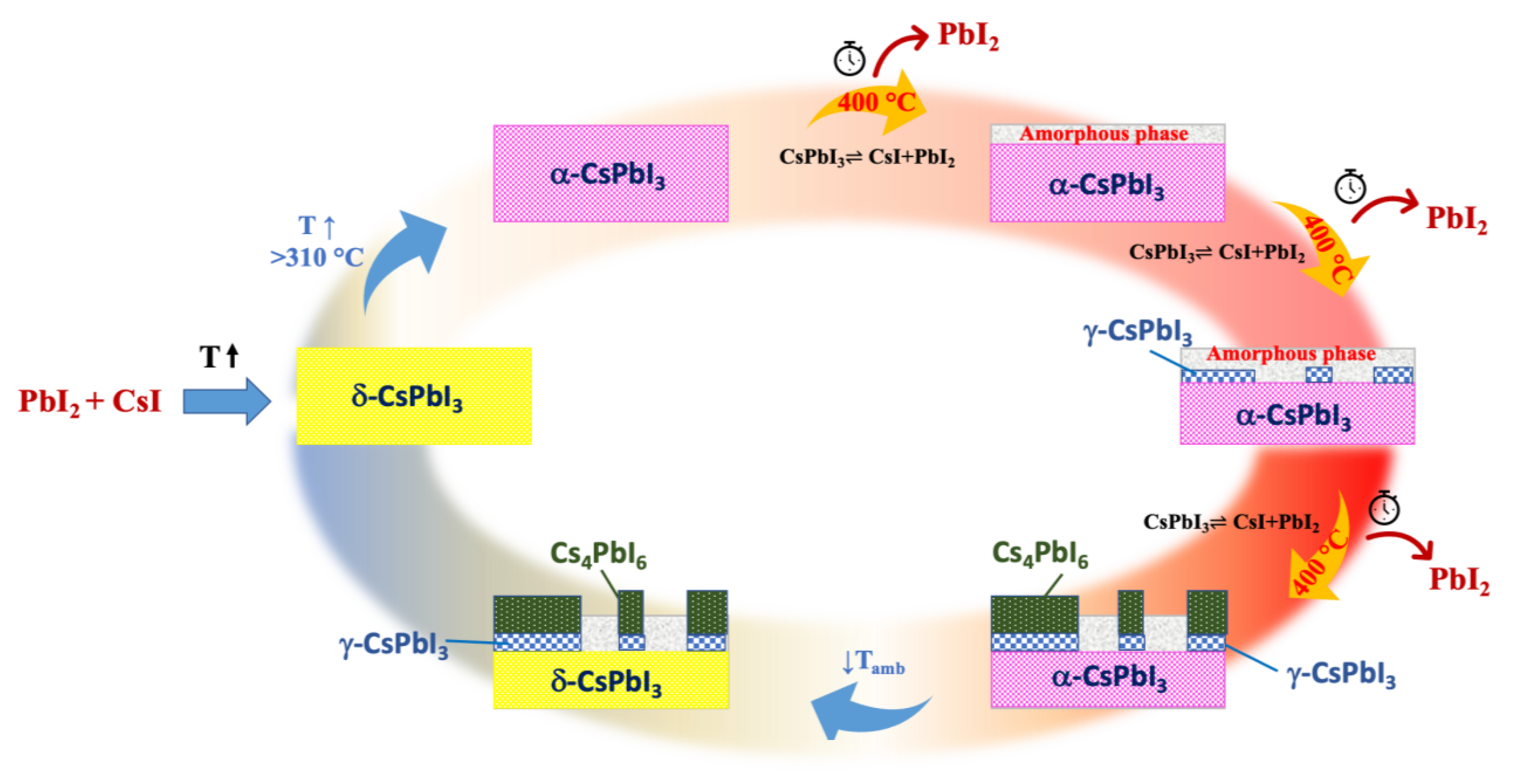
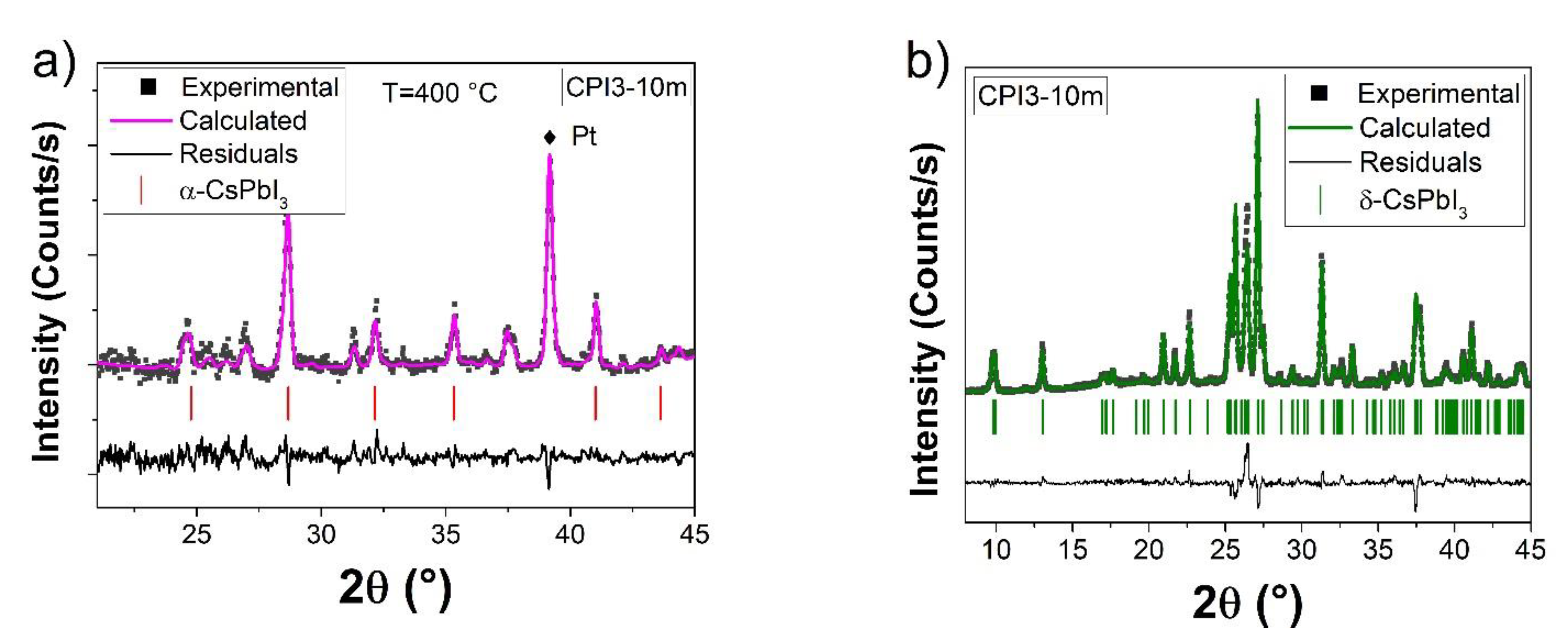
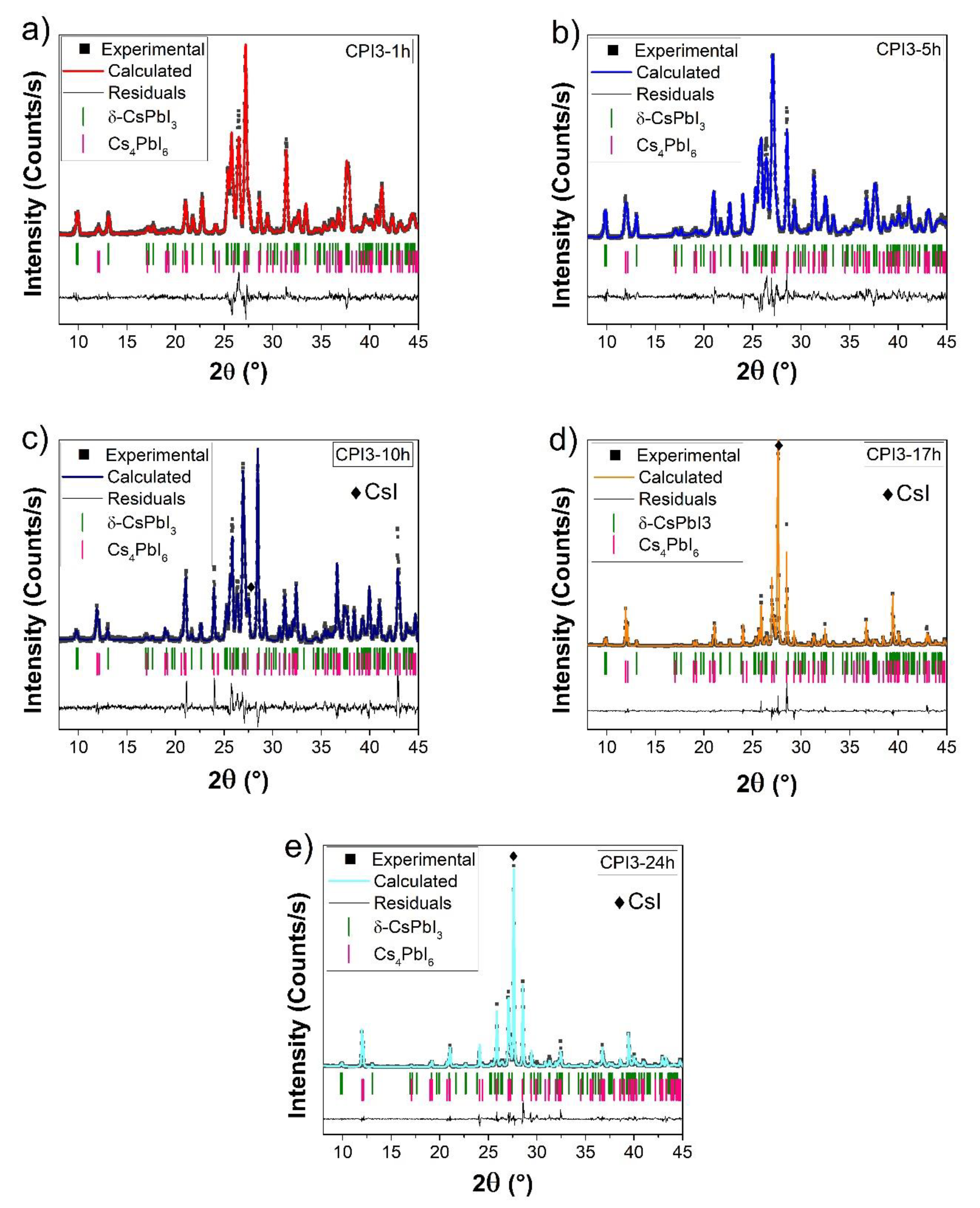
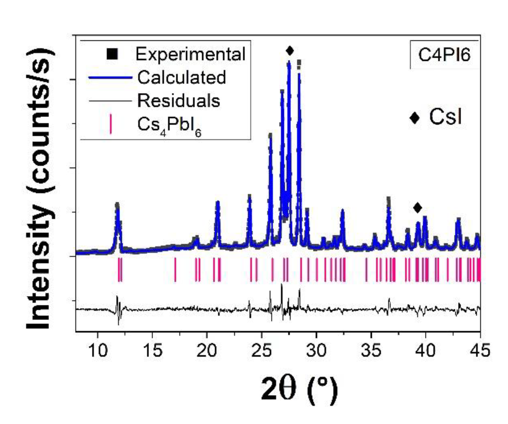
3.1. X-ray Diffraction Measurements
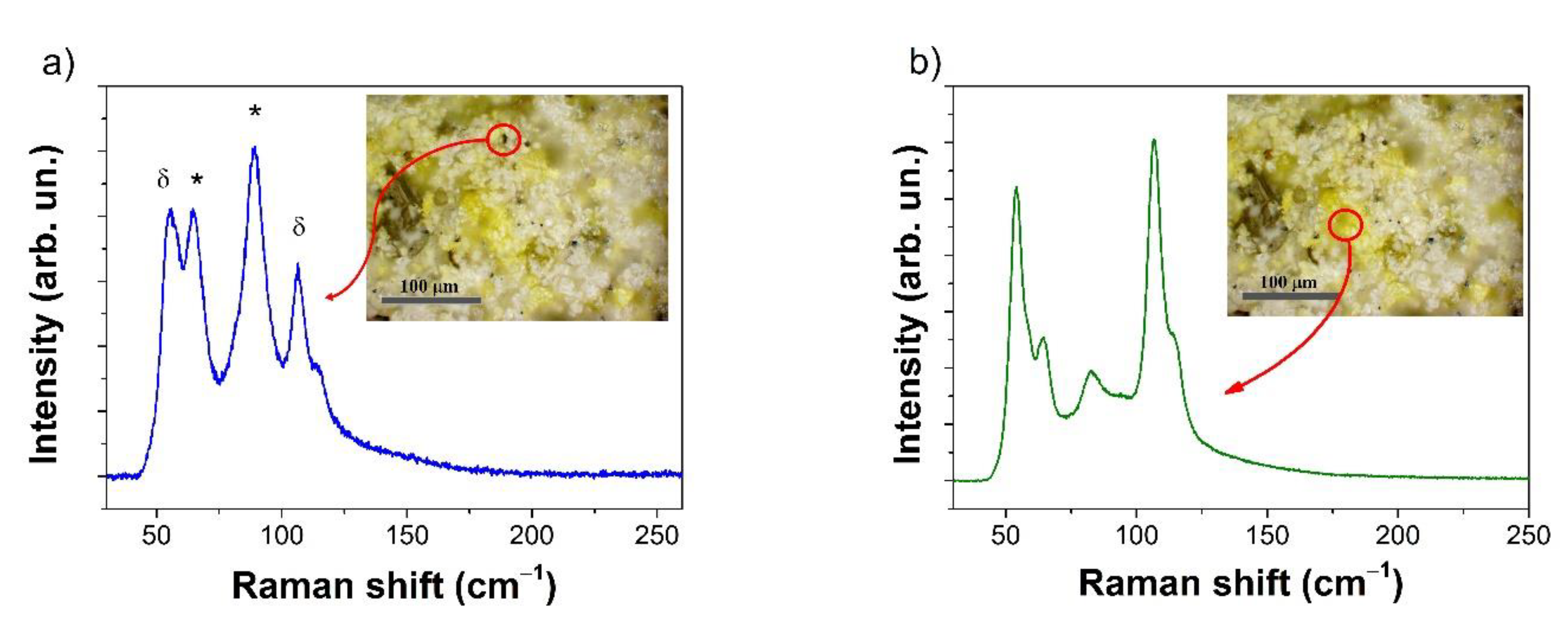
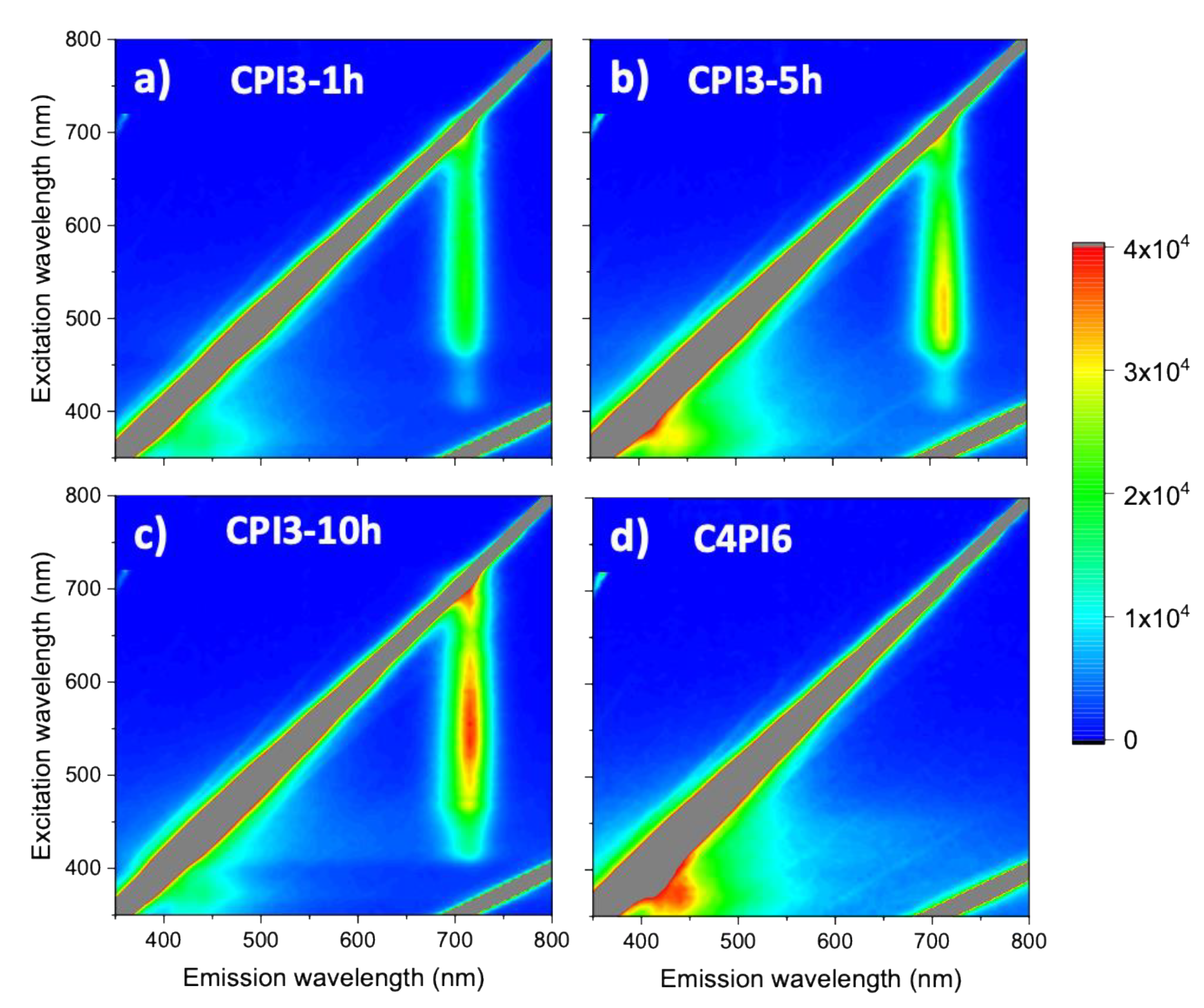
3.2. Luminescence and Raman Maps
3.3. HRTEM and Epitaxy Studies
4. Conclusions
Supplementary Materials
Author Contributions
Funding
Informed Consent Statement
Data Availability Statement
Acknowledgments
Conflicts of Interest
References
- Mitzi, D.B. Synthesis, Structure, and Properties of Organic-Inorganic Perovskites and Related Materials. In Progress in Inorganic Chemistry; Wiley: Hoboken, NJ, USA, 2007; pp. 1–121. [Google Scholar]
- Stranks, S.D.; Eperon, G.E.; Grancini, G.; Menelaou, C.; Alcocer, M.J.P.; Leijtens, T.; Herz, L.M.; Petrozza, A.; Snaith, H.J. Electron-Hole Diffusion Lengths Exceeding 1 Micrometer in an Organometal Trihalide Perovskite Absorber. Science 2013, 342, 341–344. [Google Scholar] [CrossRef] [Green Version]
- Green, M.A.; Jiang, Y.; Soufiani, A.M.; Ho-Baillie, A. Optical Properties of Photovoltaic Organic–Inorganic Lead Halide Perovskites. J. Phys. Chem. Lett. 2015, 6, 4774–4785. [Google Scholar] [CrossRef] [PubMed]
- Xing, G.; Mathews, N.; Sun, S.; Lim, S.S.; Lam, Y.M.; Gratzel, M.; Mhaisalkar, S.; Sum, T.C. Long-Range Balanced Electron- and Hole-Transport Lengths in Organic-Inorganic CH3NH3PbI3. Science 2013, 342, 344–347. [Google Scholar] [CrossRef]
- Walsh, A. Principles of Chemical Bonding and Band Gap Engineering in Hybrid Organic–Inorganic Halide Perovskites. J. Phys. Chem. C 2015, 119, 5755–5760. [Google Scholar] [CrossRef] [PubMed] [Green Version]
- Kim, H.-S.; Lee, C.-R.; Im, J.-H.; Lee, K.-B.; Moehl, T.; Marchioro, A.; Moon, S.-J.; Humphry-Baker, R.; Yum, J.-H.; Moser, J.E.; et al. Lead Iodide Perovskite Sensitized All-Solid-State Submicron Thin Film Mesoscopic Solar Cell with Efficiency Exceeding 9%. Sci. Rep. 2012, 2, 591. [Google Scholar] [CrossRef] [PubMed] [Green Version]
- Cho, H.; Kim, Y.-H.; Wolf, C.; Lee, H.-D.; Lee, T.-W. Improving the Stability of Metal Halide Perovskite Materials and Light-Emitting Diodes. Adv. Mater. 2018, 30, 1704587. [Google Scholar] [CrossRef]
- Yang, Z.; Deng, Y.; Zhang, X.; Wang, S.; Chen, H.; Yang, S.; Khurgin, J.; Fang, N.X.; Zhang, X.; Ma, R. High-Performance Single-Crystalline Perovskite Thin-Film Photodetector. Adv. Mater. 2018, 30, 1704333. [Google Scholar] [CrossRef]
- Dong, Q.; Fang, Y.; Shao, Y.; Mulligan, P.; Qiu, J.; Cao, L.; Huang, J. Electron-hole diffusion lengths >175 μm in solution-grown CH3 NH3 PbI3 single crystals. Science 2015, 347, 967–970. [Google Scholar] [CrossRef] [Green Version]
- Huang, H.; Polavarapu, L.; Sichert, J.A.; Susha, A.S.; Urban, A.S.; Rogach, A.L. Colloidal lead halide perovskite nanocrystals: Synthesis, optical properties and applications. NPG Asia Mater. 2016, 8, e328. [Google Scholar] [CrossRef] [Green Version]
- Anni, M.; Cretí, A.; De Giorgi, M.L.; De Lomascolo, M. Local Morphology Effects on the Photoluminescence Properties of Thin CsPbBr3 Nanocrystal Films. Nanomaterials 2021, 11, 1470. [Google Scholar] [CrossRef]
- Akbulatov, A.F.; Luchkin, S.Y.; Frolova, L.A.; Dremova, N.N.; Gerasimov, K.L.; Zhidkov, I.S.; Anokhin, D.V.; Kurmaev, E.Z.; Stevenson, K.J.; Troshin, P.A. Probing the Intrinsic Thermal and Photochemical Stability of Hybrid and Inorganic Lead Halide Perovskites. J. Phys. Chem. Lett. 2017, 8, 1211–1218. [Google Scholar] [CrossRef] [PubMed]
- Iagher, L.; Etgar, L. Effect of Cs on the Stability and Photovoltaic Performance of 2D/3D Perovskite-Based Solar Cells. ACS Energy Lett. 2018, 3, 366–372. [Google Scholar] [CrossRef]
- Zhou, Y.; Zhao, Y. Chemical stability and instability of inorganic halide perovskites. Energy Environ. Sci. 2019, 12, 1495–1511. [Google Scholar] [CrossRef]
- Deretzis, I.; Bongiorno, C.; Mannino, G.; Smecca, E.; Sanzaro, S.; Valastro, S.; Fisicaro, G.; Magna, A.L.; Alberti, A. Exploring the structural competition between the black and the yellow phase of cspbi3. Nanomaterials 2021, 11, 1282. [Google Scholar] [CrossRef]
- Stoumpos, C.C.; Malliakas, C.D.; Kanatzidis, M.G. Semiconducting Tin and Lead Iodide Perovskites with Organic Cations: Phase Transitions, High Mobilities, and Near-Infrared Photoluminescent Properties. Inorg. Chem. 2013, 52, 9019–9038. [Google Scholar] [CrossRef]
- Marronnier, A.; Roma, G.; Boyer-Richard, S.; Pedesseau, L.; Jancu, J.M.; Bonnassieux, Y.; Katan, C.; Stoumpos, C.C.; Kanatzidis, M.G.; Even, J. Anharmonicity and Disorder in the Black Phases of Cesium Lead Iodide Used for Stable Inorganic Perovskite Solar Cells. ACS Nano 2018, 12, 3477–3486. [Google Scholar] [CrossRef] [PubMed]
- Mehdi, H.; Mhamdi, A.; Hannachi, R.; Bouazizi, A. MAPbBr3 perovskite solar cells via a two-step deposition process. RSC Adv. 2019, 9, 12906–12912. [Google Scholar] [CrossRef] [Green Version]
- Huang, D.; Xie, P.; Pan, Z.; Rao, H.; Zhong, X. One-step solution deposition of CsPbBr3 based on precursor engineering for efficient all-inorganic perovskite solar cells. J. Mater. Chem. A 2019, 7, 22420–22428. [Google Scholar] [CrossRef]
- Konstantakou, M.; Perganti, D.; Falaras, P.; Stergiopoulos, T. Anti-Solvent Crystallization Strategies for Highly Efficient Perovskite Solar Cells. Crystals 2017, 7, 291. [Google Scholar] [CrossRef] [Green Version]
- Wang, P.; Zhang, X.; Zhou, Y.; Jiang, Q.; Ye, Q.; Chu, Z.; Li, X.; Yang, X.; Yin, Z.; You, J. Solvent-controlled growth of inorganic perovskite films in dry environment for efficient and stable solar cells. Nat. Commun. 2018, 9, 2225. [Google Scholar] [CrossRef]
- Li, B.; Zhang, Y.; Fu, L.; Yu, T.; Zhou, S.; Zhang, L.; Yin, L. Surface passivation engineering strategy to fully-inorganic cubic CsPbI3 perovskites for high-performance solar cells. Nat. Commun. 2018, 9, 1076. [Google Scholar] [CrossRef] [PubMed]
- Luo, P.; Xia, W.; Zhou, S.; Sun, L.; Cheng, J.; Xu, C.; Lu, Y. Solvent Engineering for Ambient-Air-Processed, Phase-Stable CsPbI3 in Perovskite Solar Cells. J. Phys. Chem. Lett. 2016, 7, 3603–3608. [Google Scholar] [CrossRef]
- Xiang, S.; Fu, Z.; Li, W.; Wei, Y.; Liu, J.; Liu, H.; Zhu, L.; Zhang, R.; Chen, H. Highly Air-Stable Carbon-Based α-CsPbI3 Perovskite Solar Cells with a Broadened Optical Spectrum. ACS Energy Lett. 2018, 3, 1824–1831. [Google Scholar] [CrossRef]
- Protesescu, L.; Yakunin, S.; Bodnarchuk, M.I.; Krieg, F.; Caputo, R.; Hendon, C.H.; Yang, R.X.; Walsh, A.; Kovalenko, M.V. Nanocrystals of Cesium Lead Halide Perovskites (CsPbX3, X = Cl, Br, and I): Novel Optoelectronic Materials Showing Bright Emission with Wide Color Gamut. Nano Lett. 2015, 15, 3692–3696. [Google Scholar] [CrossRef] [Green Version]
- Ke, W.; Spanopoulos, I.; Stoumpos, C.C.; Kanatzidis, M.G. Myths and reality of HPbI3 in halide perovskite solar cells. Nat. Commun. 2018, 9, 4785. [Google Scholar] [CrossRef]
- El Ajjouri, Y.; Palazon, F.; Sessolo, M.; Bolink, H.J. Single-Source Vacuum Deposition of Mechanosynthesized Inorganic Halide Perovskites. Chem. Mater. 2018, 30, 7423–7427. [Google Scholar] [CrossRef] [Green Version]
- Karmakar, A.; Dodd, M.S.; Zhang, X.; Oakley, M.S.; Klobukowski, M.; Michaelis, V.K. Mechanochemical synthesis of 0D and 3D cesium lead mixed halide perovskites. Chem. Commun. 2019, 55, 5079–5082. [Google Scholar] [CrossRef] [PubMed]
- Hong, Z.; Tan, D.; John, R.A.; Tay, Y.K.E.; Ho, Y.K.T.; Zhao, X.; Sum, T.C.; Mathews, N.; García, F.; Soo, H. Sen Completely Solvent-free Protocols to Access Phase-Pure, Metastable Metal Halide Perovskites and Functional Photodetectors from the Precursor Salts. iScience 2019, 16, 312–325. [Google Scholar] [CrossRef] [PubMed] [Green Version]
- Straus, D.B.; Guo, S.; Cava, R.J. Kinetically Stable Single Crystals of Perovskite-Phase CsPbI3. J. Am. Chem. Soc. 2019, 141, 11435–11439. [Google Scholar] [CrossRef] [Green Version]
- Satta, J.; Melis, C.; Carbonaro, C.M.; Pinna, A.; Salado, M.; Salazar, D.; Ricci, P.C. Raman spectra and vibrational analysis of CsPbI3: A fast and reliable technique to identify lead halide perovskite polymorphs. J. Mater. 2021, 7, 127–135. [Google Scholar] [CrossRef]
- Lutterotti, L. Total pattern fitting for the combined size–strain–stress–texture determination in thin film diffraction. Nucl. Instrum. Methods Phys. Res. Sect. B Beam Interact. Mater. Atoms 2010, 268, 334–340. [Google Scholar] [CrossRef]
- Zhang, Q.; Zhou, Y.; Wei, Y.; Tai, M.; Nan, H.; Gu, Y.; Han, J.; Yin, X.; Li, J.; Lin, H. Improved phase stability of γ-CsPbI 3 perovskite nanocrystals using the interface effect using iodine modified graphene oxide. J. Mater. Chem. C 2020, 8, 2569–2578. [Google Scholar] [CrossRef]
- Sutton, R.J.; Filip, M.R.; Haghighirad, A.A.; Sakai, N.; Wenger, B.; Giustino, F.; Snaith, H.J. Cubic or Orthorhombic? Revealing the Crystal Structure of Metastable Black-Phase CsPbI3 by Theory and Experiment. ACS Energy Lett. 2018, 3, 1787–1794. [Google Scholar] [CrossRef]
- Yang, Y.; Robbins, J.P.; Ezeonu, L.; Ma, Y.; Sparta, N.; Kong, X.; Strauf, S.; Podkolzin, S.G.; Lee, S.S. Probing lattice vibrations of stabilized CsPbI3 polymorphs via low-frequency Raman spectroscopy. J. Mater. Chem. C 2020, 8, 8896–8903. [Google Scholar] [CrossRef]
- Liu, F.; Zhang, Y.; Ding, C.; Kobayashi, S.; Izuishi, T.; Nakazawa, N.; Toyoda, T.; Ohta, T.; Hayase, S.; Minemoto, T.; et al. Highly Luminescent Phase-Stable CsPbI 3 Perovskite Quantum Dots Achieving Near 100% Absolute Photoluminescence Quantum Yield. ACS Nano 2017, 11, 10373–10383. [Google Scholar] [CrossRef]
- Zhao, B.; Jin, S.-F.; Huang, S.; Liu, N.; Ma, J.-Y.; Xue, D.-J.; Han, Q.; Ding, J.; Ge, Q.-Q.; Feng, Y.; et al. Thermodynamically Stable Orthorhombic γ-CsPbI3 Thin Films for High-Performance Photovoltaics. J. Am. Chem. Soc. 2018, 140, 11716–11725. [Google Scholar] [CrossRef] [PubMed]
- Babin, V.; Krasnikov, A.; Nikl, M.; Nitsch, K.; Stolovits, A.; Zazubovich, S. Luminescence and relaxed excited state origin in CsI:Pb crystals. J. Lumin. 2003, 101, 219–226. [Google Scholar] [CrossRef]
- Chen, C.; Zhang, L.; Shi, T.; Liao, G.; Tang, Z. Controllable synthesis of all inorganic lead halide perovskite nanocrystals with various appearances in multiligand reaction system. Nanomaterials 2019, 9, 1751. [Google Scholar] [CrossRef] [Green Version]
- Lakowicz, J.R. Principles of Fluorescence Spectroscopy; Lakowicz, J.R., Ed.; Springer: Boston, MA, USA, 2006; ISBN 978-0-387-31278-1. [Google Scholar]
- Becker, P.; Márquez, J.A.; Just, J.; Al-Ashouri, A.; Hages, C.; Hempel, H.; Jošt, M.; Albrecht, S.; Frahm, R.; Unold, T. Low Temperature Synthesis of Stable γ-CsPbI3 Perovskite Layers for Solar Cells Obtained by High Throughput Experimentation. Adv. Energy Mater. 2019, 9, 1900555. [Google Scholar] [CrossRef] [Green Version]


| Time | Phases | Rwp | RB | |
|---|---|---|---|---|
| δ-CsPbI3 | Cs4PbI6 | |||
| 10 min | 100% | 10.5% | 8.0% | |
| 1 h | 90.6% | 9.4% | 12.1% | 9.6% |
| 5 h | 54.9% | 45.1% | 12.6% | 9.8% |
| 10 h | 42.1% | 57.9% | 13.6% | 10.6% |
| 17 h | 33.2% | 66.8% | 12.8% | 8.9% |
| 24 h | 21.5% | 78.5% | 17.6% | 12.6% |
| Sample | CPI3-1 h | CPI3-5 h | CPI3-10 h | CPI3-17 h | CPI3-24 h |
|---|---|---|---|---|---|
| Synthesis time | 1 h | 5 h | 10 h | 17 h | 24 h |
| Quantum yield | 0.6% | 0.7% | 1.86% | 0.5% | 0% |
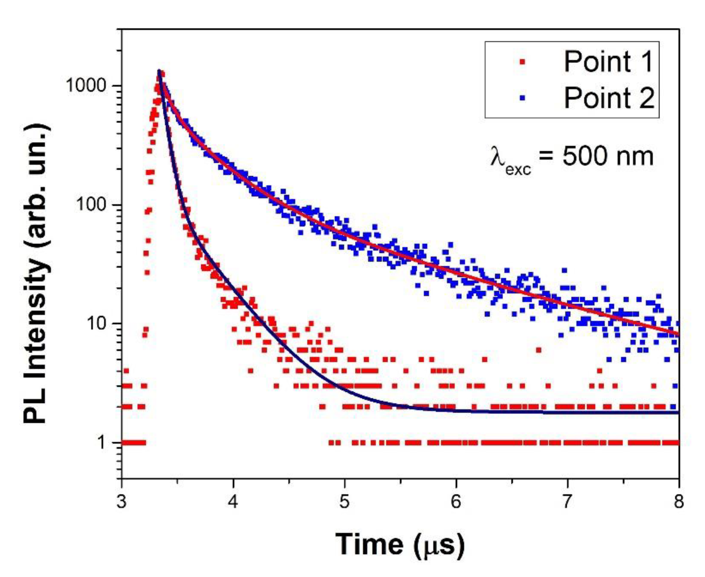
| A1 | τ1 (μs) | A2 | τ2 (μs) | A3 | τ3 (μs) | ||
|---|---|---|---|---|---|---|---|
| Point 1 | 0.144 | 1,823.671 | 0.060 | 131.900 | 0.346 | - | - |
| Point 2 | 0.908 | 448.511 | 0.093 | 497.428 | 0.399 | 136.149 | 1.548 |
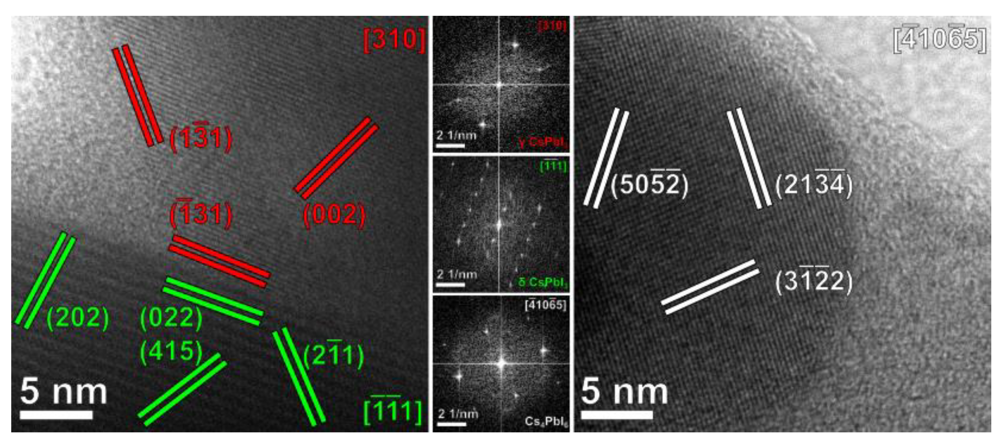
| Commensurate Lattice Mismatches m | |
|---|---|
| δ-phase//γ-phase | m |
| 6 *(0 2 2)//8 *(−1 3 1) | 4.0% |
| (2 −1 1)//(1 −3 1) | 1.0% |
| 3 *(−1 −1 1)//4 *(3 1 0) | 2.0% |
Publisher’s Note: MDPI stays neutral with regard to jurisdictional claims in published maps and institutional affiliations. |
© 2021 by the authors. Licensee MDPI, Basel, Switzerland. This article is an open access article distributed under the terms and conditions of the Creative Commons Attribution (CC BY) license (https://creativecommons.org/licenses/by/4.0/).
Share and Cite
Satta, J.; Casu, A.; Chiriu, D.; Carbonaro, C.M.; Stagi, L.; Ricci, P.C. Formation Mechanisms and Phase Stability of Solid-State Grown CsPbI3 Perovskites. Nanomaterials 2021, 11, 1823. https://doi.org/10.3390/nano11071823
Satta J, Casu A, Chiriu D, Carbonaro CM, Stagi L, Ricci PC. Formation Mechanisms and Phase Stability of Solid-State Grown CsPbI3 Perovskites. Nanomaterials. 2021; 11(7):1823. https://doi.org/10.3390/nano11071823
Chicago/Turabian StyleSatta, Jessica, Alberto Casu, Daniele Chiriu, Carlo Maria Carbonaro, Luigi Stagi, and Pier Carlo Ricci. 2021. "Formation Mechanisms and Phase Stability of Solid-State Grown CsPbI3 Perovskites" Nanomaterials 11, no. 7: 1823. https://doi.org/10.3390/nano11071823
APA StyleSatta, J., Casu, A., Chiriu, D., Carbonaro, C. M., Stagi, L., & Ricci, P. C. (2021). Formation Mechanisms and Phase Stability of Solid-State Grown CsPbI3 Perovskites. Nanomaterials, 11(7), 1823. https://doi.org/10.3390/nano11071823