
Size-Dependent Electrical Transport Properties in Conducting Diamond Nanostripes


Abstract
:1. Introduction
2. Materials and Methods
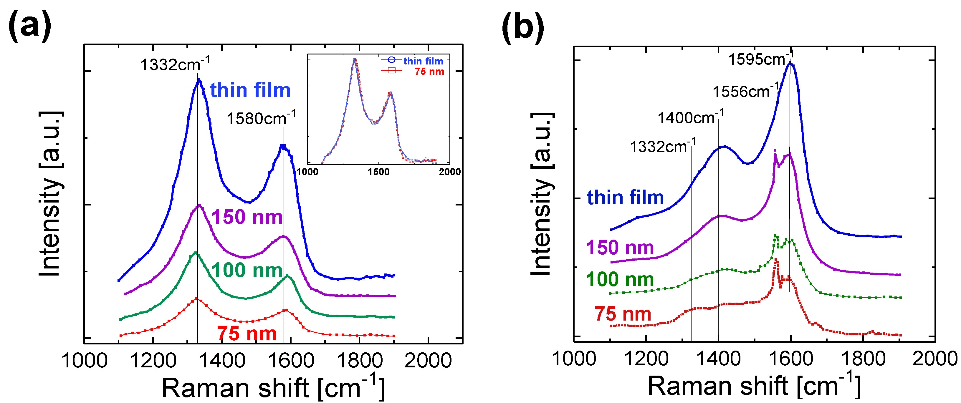
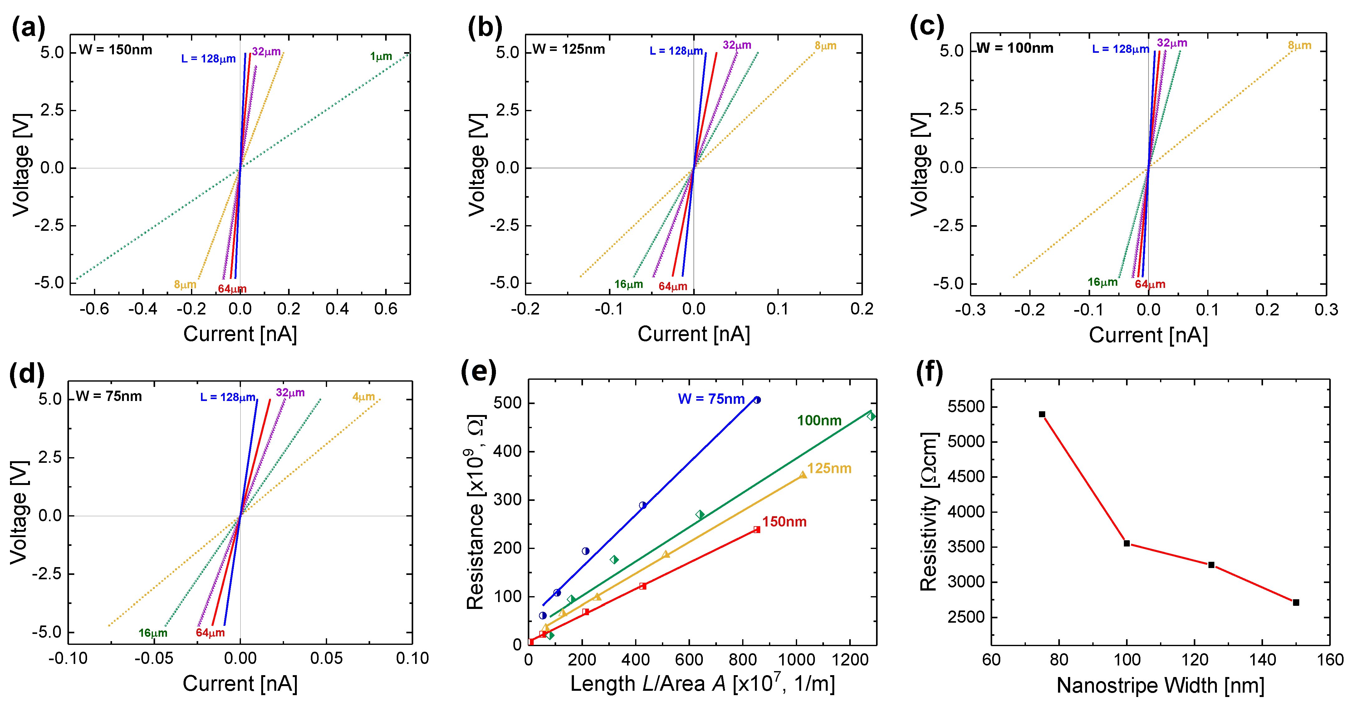
3. Results and Discussion
4. Conclusions
Author Contributions
Funding
Data Availability Statement
Acknowledgments
Conflicts of Interest
References
- Jiao, S.; Sumant, A.; Kirk, M.A.; Gruen, D.M.; Krauss, A.R.; Auciello, O. Microstructure of ultrananocrystalline diamond films grown by microwave Ar–CH4 plasma chemical vapor deposition with or without added H2. J. Appl. Phys. 2001, 90, 118–122. [Google Scholar] [CrossRef]
- Williams, O.A.; Curat, S.; Gerbi, J.E.; Gruen, D.M.; Jackman, R.B. n-type conductivity in ultrananocrystalline diamond films. Appl. Phys. Lett. 2004, 85, 1680. [Google Scholar] [CrossRef]
- Feng, P.; Wang, X.; Aldalbahi, A.; Zhou, A.F. Methane induced electrical property change of nitrogen doped ultrananocrys-talline diamond nanowires. Appl. Phys. Lett. 2013, 107, 233103. [Google Scholar] [CrossRef]
- Zhou, A.F.; Wang, X.; Feng, X.P. Nitrogen-doped Diamond Nanowire Gas Sensor for the Detection of Methane. Adv. Mater. Lett. 2020, 11, 20021473. [Google Scholar] [CrossRef]
- Peng, X.; Li, Y.; Duan, S.; Chu, J.; Feng, P. Precise ultrananocrystalline diamond nanowire arrays for high performance gas sensing application. Mater. Lett. 2020, 265, 127404. [Google Scholar] [CrossRef]
- Zhou, A.F.; Velázquez, R.; Wang, X.; Feng, P.X. Nanoplasmonic 1D Diamond UV Photodetectors with High Performance. ACS Appl. Mater. Interfaces 2019, 11, 38068–38074. [Google Scholar] [CrossRef]
- Feng, P.X.; Zhang, H.X.; Peng, X.Y.; Sajjad, M.; Chu, J. A novel compact design of calibration equipment for gas and thermal sensors. Rev. Sci. Instrum. 2011, 82, 043303. [Google Scholar] [CrossRef] [PubMed]
- Zhou, A.; Wang, X.; Pacheco, E.; Feng, P. Ultrananocrystalline Diamond Nanowires: Fabrication, Characterization, and Sensor Applications. Materials 2021, 14, 661. [Google Scholar] [CrossRef]
- Bhattacharyya, S.; Auciello, O.; Birrell, J.; Carlisle, J.; Curtiss, L.; Goyette, A.N.; Gruen, D.M.; Krauss, A.R.; Schlueter, J.; Sumant, A.V.; et al. Synthesis and characterization of highly-conducting nitrogen-doped ultrananocrystalline diamond films. Appl. Phys. Lett. 2001, 79, 1441–1443. [Google Scholar] [CrossRef]
- Wang, X.; Ocola, L.; Divan, R.S.; Sumant, A.V. Nanopatterning of ultrananocrystalline diamond nanowires. Nanotechnology 2012, 23, 075301. [Google Scholar] [CrossRef]
- Achatz, P.; Williams, O.A.; Bruno, P.; Gruen, D.M.; Garrido, J.A.; Stutzmann, M.; Achatz, P.; Williams, O.A.; Bruno, P.; Gruen, D.M.; et al. Effect of nitrogen on the electronic properties of ultrananocrystalline diamond thin films grown on quartz and diamond substrates. Phys. Rev. B 2006, 74, 155429. [Google Scholar] [CrossRef]
- Bhattacharyya, S. Mechanism of high n-type conduction in nitrogen-doped nanocrystalline diamond. Phys. Rev. B 2004, 70, 125412. [Google Scholar] [CrossRef]
- Birrell, J.; Gerbi, J.E.; Auciello, O.; Gibson, J.M.; Johnson, J.; Carlisle, J.A. Interpretation of the Raman spectra of ultranano-crystalline diamond. Diam. Relat. Mater. 2005, 14, 86–92. [Google Scholar] [CrossRef]
- Obraztsov, A.N.; Tyurnina, A.V.; Obraztsova, E.A.; Zolotukhin, A.A.; Liu, B.; Chin, K.-C.; Wee, A.T. Raman scattering characterization of CVD graphite films. Carbon 2008, 46, 963–968. [Google Scholar] [CrossRef]
- Weber, A.; McGinnis, E.A. The Raman spectrum of gaseous oxygen. J. Mol. Spectrosc. 1960, 4, 195–200. [Google Scholar] [CrossRef]
- Fletcher, W.H.; Rayside, J.S. High resolution vibrational Raman spectrum of oxygen. J. Raman Spectrosc. 1974, 2, 3–14. [Google Scholar] [CrossRef]
- Feng, P.X.; Aldalbahi, A. A compact design of a characterization station for far UV photodetectors. Rev. Sci. Instrum. 2018, 89, 015001. [Google Scholar] [CrossRef]
- Yoo, E.; Moon, J.H.; Jeon, Y.S.; Kim, Y.; Ahn, J.-P.; Kim, Y.K. Electrical resistivity and microstructural evolution of electrodeposited Co and Co-W nanowires. Mater. Charact. 2020, 116, 110451. [Google Scholar] [CrossRef]
- Shalini, J.; Lin, Y.-C.; Chang, T.-H.; Sankaran, K.J.; Chen, H.-C.; Lin, I.-N.; Lee, C.-Y.; Tai, N.-H. Ultra-nanocrystalline diamond nanowires with enhanced electrochemical properties. Electrochim. Acta 2013, 92, 9–19. [Google Scholar] [CrossRef]
- Nikhar, T.; Rechenberg, R.; Becker, M.; Baryshev, S.V. Revisiting Effects of Nitrogen Incorporation and Graphitization on Conductivity of Ultra-nano-crystalline Diamond Films. arXiv 2019, arXiv:1910.09595. [Google Scholar]
- Arenal, R.; Bruno, P.; Miller, D.J.; Bleuel, M.; Lal, J.; Gruen, D.M. Diamond nanowires and the insulator-metal transition in ultrananocrystalline diamond films. Phys. Rev. B 2007, 75, 195431. [Google Scholar] [CrossRef] [Green Version]
- Garrett, D.J.; Ganesan, K.; Stacey, A.; Fox, K.; Meffin, H.; Prawer, S. Ultra-nanocrystalline diamond electrodes: Optimization towards neural stimulation applications. J. Neural Eng. 2011, 9, 016002. [Google Scholar] [CrossRef] [PubMed]
- Van Beveren, L.H.W.; Creedon, D.L.; Eikenberg, N.; Ganesan, K.; Johnson, B.C.; Chimowa, G.; Churochkin, D.; Bhattacharyya, S.; Prawer, S. Anisotropic three-dimensional weak localization in ultrananocrystalline diamond films with nitrogen inclusions. Phys. Rev. B 2020, 101, 115306. [Google Scholar] [CrossRef] [Green Version]
- Sun, T.; Yao, B.; Warren, A.P.; Barmak, K.; Toney, M.F.; Peale, R.E.; Coffey, K.R. Dominant role of grain boundary scattering in the resistivity of nanometric Cu films. Phys. Rev. B 2009, 79, 041402. [Google Scholar] [CrossRef]


| 5% N2 Present in Plasma | Conductivity σ (Ω cm)−1 | Resistivity ρ (Ω cm) | Reference |
|---|---|---|---|
| Thin Film | 0.1 | (10) | [9] |
| Thin Film | 13.20 | (0.0758) | [19] |
| Thin Film | (1.69 × 10⁻³–111) | 0.009–590.2 | [20] |
| Thin Film | 0.14 | (7.14) | [21] |
| Thin Film | 7.5 | (0.133) | [22] |
| Thin Film | 0.01 | (100) | [23] |
| 150 nm wide NS | 3.68 × 10⁻⁴ | 2.72 × 10³ | This work |
| 75 nm wide NS | 1.85 × 10⁻⁴ | 5.40 × 10³ | This work |
Publisher’s Note: MDPI stays neutral with regard to jurisdictional claims in published maps and institutional affiliations. |
© 2021 by the authors. Licensee MDPI, Basel, Switzerland. This article is an open access article distributed under the terms and conditions of the Creative Commons Attribution (CC BY) license (https://creativecommons.org/licenses/by/4.0/).
Share and Cite
Zhou, A.F.; Pacheco, E.; Zhou, B.; Feng, P.X. Size-Dependent Electrical Transport Properties in Conducting Diamond Nanostripes. Nanomaterials 2021, 11, 1765. https://doi.org/10.3390/nano11071765
Zhou AF, Pacheco E, Zhou B, Feng PX. Size-Dependent Electrical Transport Properties in Conducting Diamond Nanostripes. Nanomaterials. 2021; 11(7):1765. https://doi.org/10.3390/nano11071765
Chicago/Turabian StyleZhou, Andrew F., Elluz Pacheco, Badi Zhou, and Peter X. Feng. 2021. "Size-Dependent Electrical Transport Properties in Conducting Diamond Nanostripes" Nanomaterials 11, no. 7: 1765. https://doi.org/10.3390/nano11071765
APA StyleZhou, A. F., Pacheco, E., Zhou, B., & Feng, P. X. (2021). Size-Dependent Electrical Transport Properties in Conducting Diamond Nanostripes. Nanomaterials, 11(7), 1765. https://doi.org/10.3390/nano11071765