
Graphene Nanoribbon Gap Waveguides for Dispersionless and Low-Loss Propagation with Deep-Subwavelength Confinement


 , , and
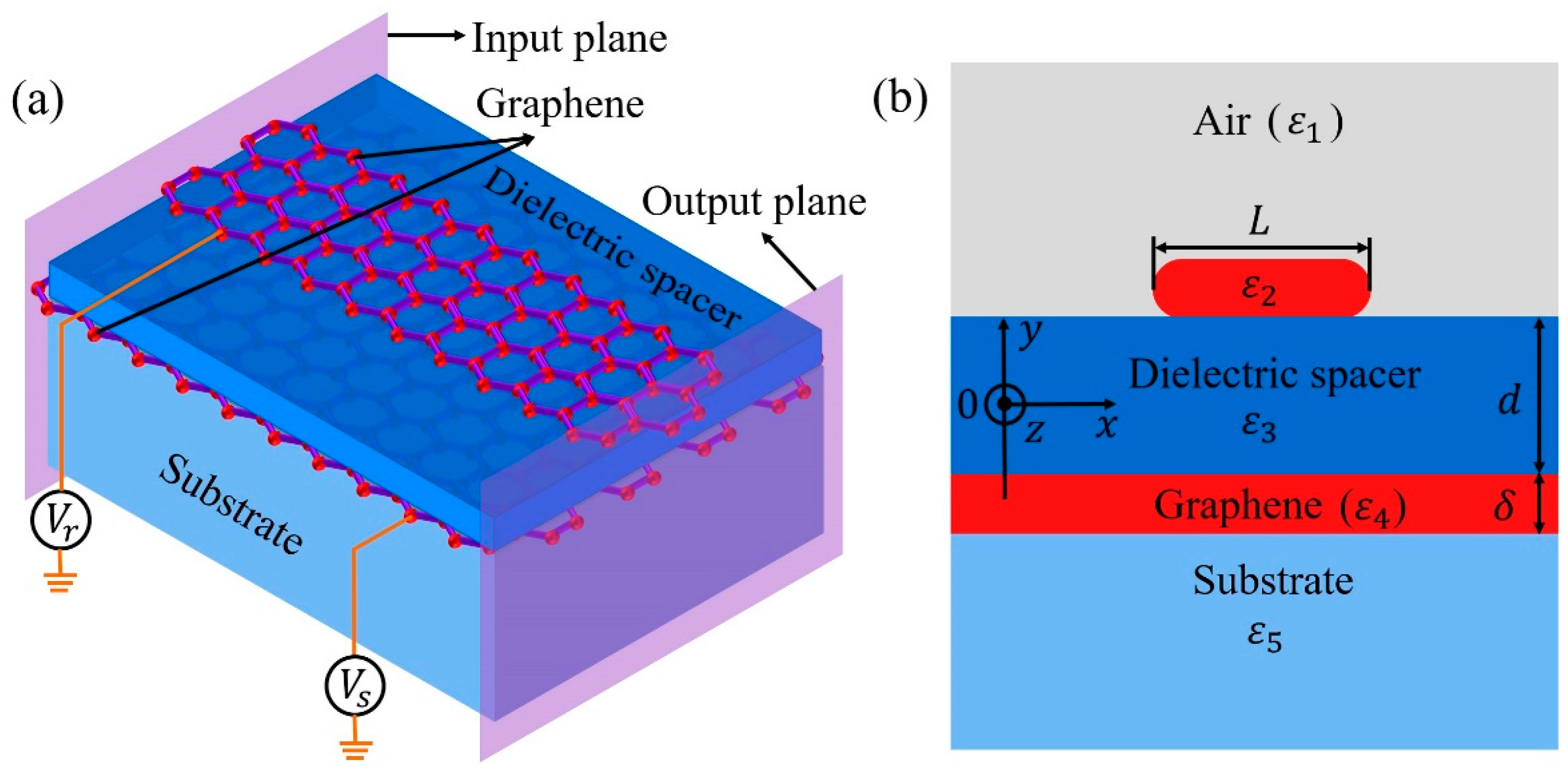
Abstract
1. Introduction
2. Theoretical Model and Method
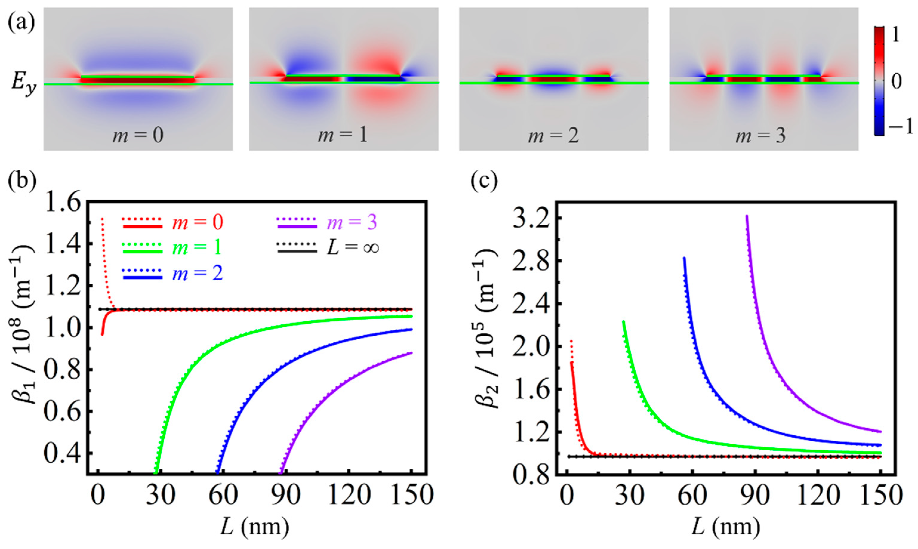
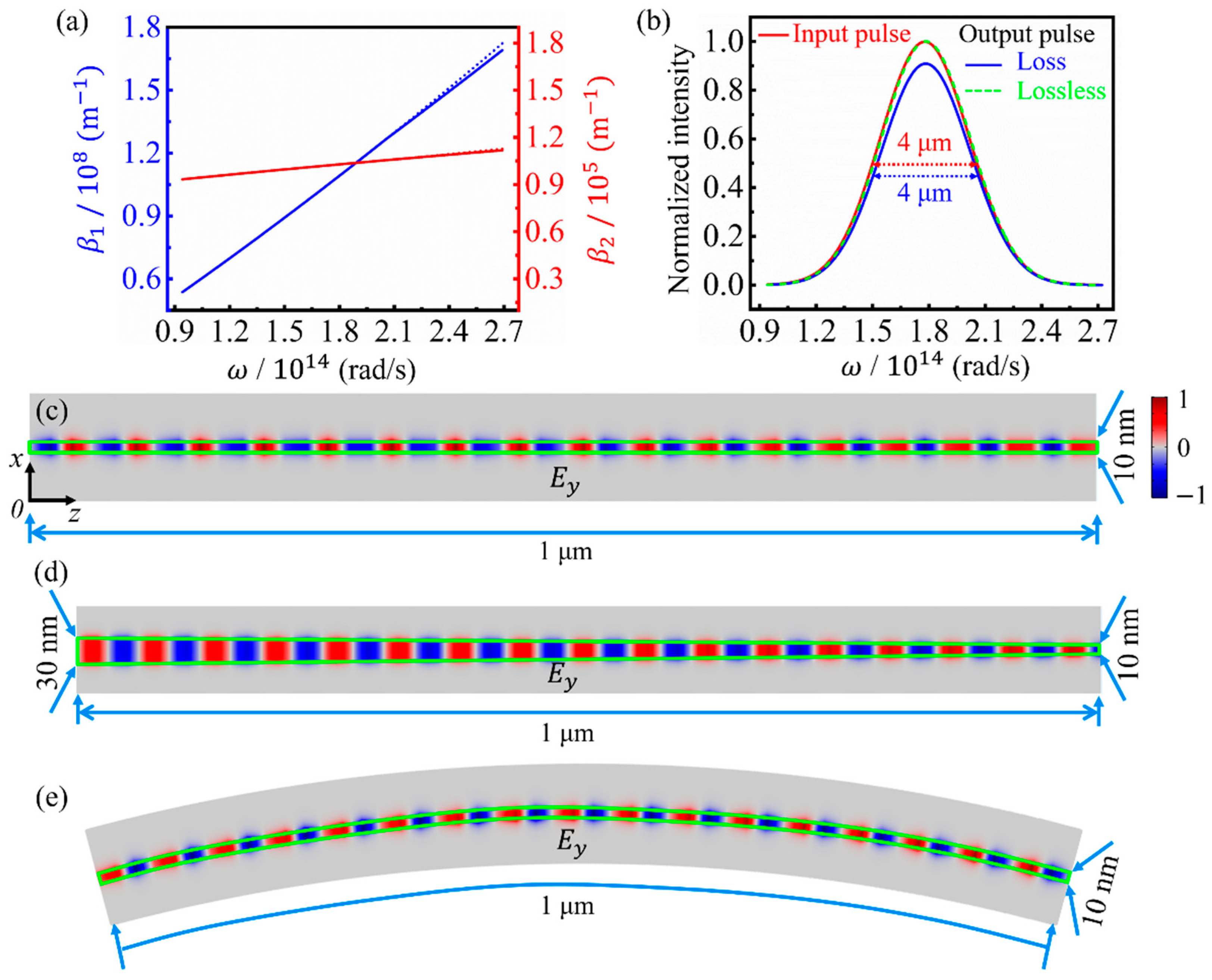
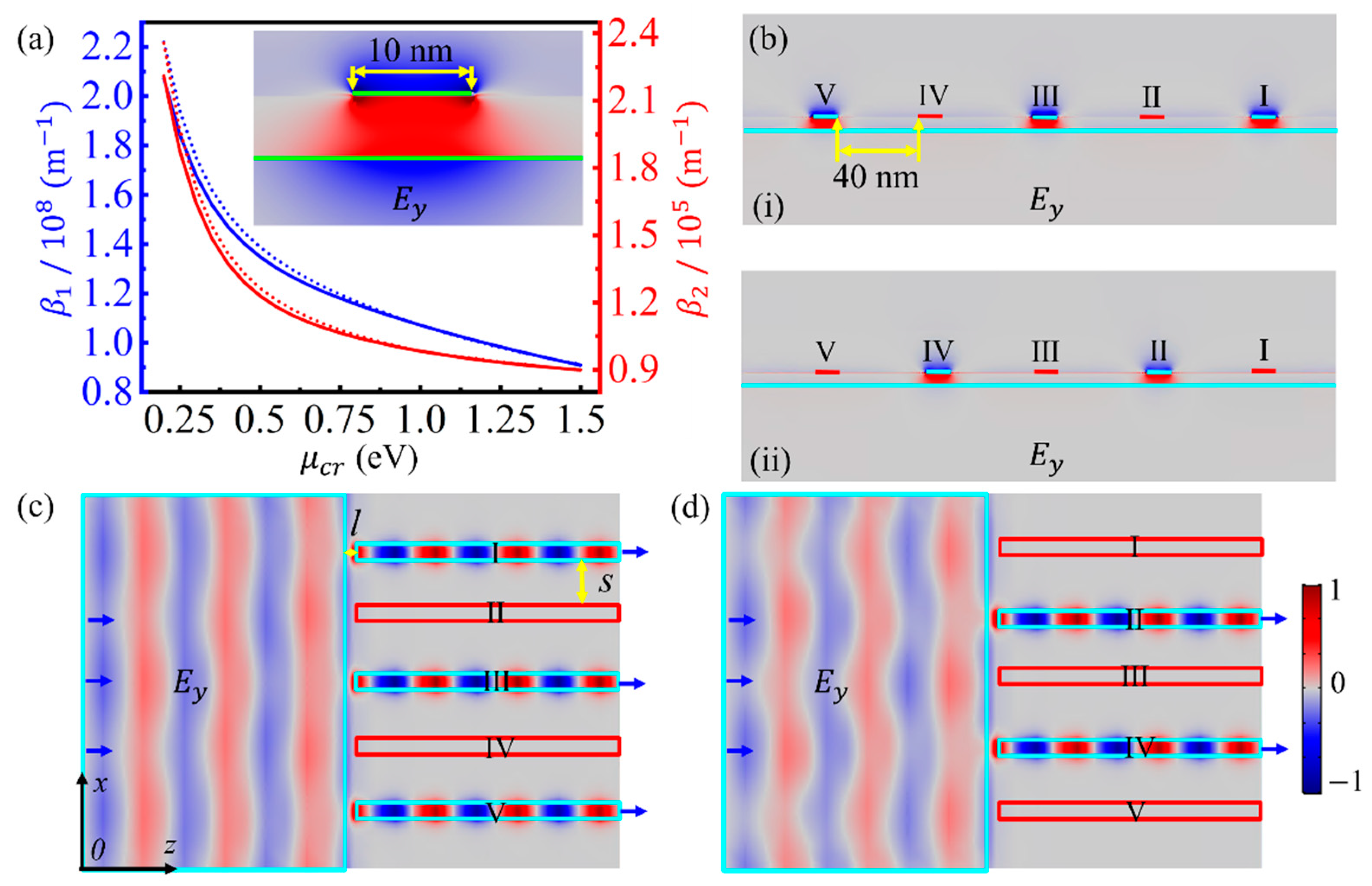
3. Results and Discussion
4. Conclusions
Supplementary Materials
Author Contributions
Funding
Data Availability Statement
Conflicts of Interest
References
- Karalis, A.; Joannopoulos, J.D.; Soljacic, M. Plasmonic-Dielectric Systems for High-Order Dispersionless Slow or Stopped Subwavelength Light. Phys. Rev. Lett. 2009, 103, 043906. [Google Scholar] [CrossRef] [PubMed]
- Guo, Y.; Jafari, Z.; Agarwal, A.M.; Kimerling, L.C.; Li, G.; Michel, J.; Zhang, L. Bilayer dispersion-flattened waveguides with four zero-dispersion wavelengths. Opt. Lett. 2016, 41, 4939–4942. [Google Scholar] [CrossRef] [PubMed]
- Guo, Y.H.; Jafari, Z.; Xu, L.J.; Bao, C.J.; Liao, P.C.; Li, G.F.; Agarwal, A.M.; Kimerling, L.C.; Michel, J.; Willner, A.E.; et al. Ultra-flat dispersion in an integrated waveguide with five and six zero-dispersion wavelengths for mid-infrared photonics. Photonics Res. 2019, 7, 1279–1286. [Google Scholar] [CrossRef]
- Pitarke, J.M.; Silkin, V.M.; Chulkov, E.V.; Echenique, P.M. Theory of surface plasmons and surface-plasmon polaritons. Rep. Prog. Phys. 2006, 70, 1–87. [Google Scholar] [CrossRef]
- Teng, D.; Wang, K. Theoretical Analysis of Terahertz Dielectric-Loaded Graphene Waveguide. Nanomaterials 2021, 11, 210. [Google Scholar] [CrossRef]
- Unutmaz, M.A.; Unlu, M. Terahertz Spoof Surface Plasmon Polariton Waveguides: A Comprehensive Model with Experimental Verification. Sci. Rep. 2019, 9, 8. [Google Scholar] [CrossRef]
- Gramotnev, D.K.; Bozhevolnyi, S.I. Plasmonics beyond the diffraction limit. Nat. Photonics 2010, 4, 83–91. [Google Scholar] [CrossRef]
- Chau, Y.F.C.; Chao, C.T.C.; Huang, H.J.; Kooh, M.R.R.; Kumara, N.; Lim, C.M.; Chiang, H.P. Ultrawide Bandgap and High Sensitivity of a Plasmonic Metal-Insulator-Metal Waveguide Filter with Cavity and Baffles. Nanomaterials 2020, 10, 2030. [Google Scholar] [CrossRef]
- Gerislioglu, B.; Dong, L.L.; Ahmadivand, A.; Hu, H.T.; Nordlander, P.; Halas, N.J. Monolithic Metal Dimer-on-Film Structure: New Plasmonic Properties Introduced by the Underlying Metal. Nano. Lett. 2020, 20, 2087–2093. [Google Scholar] [CrossRef]
- Ahmadivand, A.; Gerislioglu, B.; Ramezani, Z. Gated graphene island-enabled tunable charge transfer plasmon terahertz metamodulator. Nanoscale 2019, 11, 8091–8095. [Google Scholar] [CrossRef]
- Butt, M.A.; Khonina, S.N.; Kazanskiy, N.L. Plasmonics: A Necessity in the Field of Sensing-A Review (Invited). Fiber Integr. Opt. 2021, 1–34. [Google Scholar] [CrossRef]
- Oulton, R.F.; Sorger, V.J.; Genov, D.A.; Pile, D.F.P.; Zhang, X. A hybrid plasmonic waveguide for subwavelength confinement and long-range propagation. Nat. Photonics 2008, 2, 496–500. [Google Scholar] [CrossRef]
- Zhang, S.; Xu, H. Optimizing Substrate-Mediated Plasmon Coupling toward High-Performance Plasmonic Nanowire Waveguides. Acs Nano 2012, 6, 8128–8135. [Google Scholar] [CrossRef] [PubMed]
- Sun, Y.; Zheng, Z.; Cheng, J.T.; Liu, J.W.; Liu, J.S.; Li, S.N. The un-symmetric hybridization of graphene surface plasmons incorporating graphene sheets and nano-ribbons. Appl. Phys. Lett. 2013, 103, 3. [Google Scholar] [CrossRef]
- Bozhevolnyi, S.I.; Volkov, V.S.; Devaux, E.; Ebbesen, T.W. Channel plasmon-polariton guiding by subwavelength metal grooves. Phys. Rev. Lett. 2005, 95, 4. [Google Scholar] [CrossRef] [PubMed]
- Bozhevolnyi, S.I.; Volkov, V.S.; Devaux, E.; Laluet, J.Y.; Ebbesen, T.W. Channel plasmon subwavelength waveguide components including interferometers and ring resonators. Nature 2006, 440, 508–511. [Google Scholar] [CrossRef]
- Pile, D.F.P.; Ogawa, T.; Gramotnev, D.K.; Okamoto, T.; Haraguchi, M.; Fukui, M.; Matsuo, S. Theoretical and experimental investigation of strongly localized plasmons on triangular metal wedges for subwavelength waveguiding. Appl. Phys. Lett. 2005, 87, 061106. [Google Scholar] [CrossRef]
- Moreno, E.; Rodrigo, S.G.; Bozhevolnyi, S.I.; Martin-Moreno, L.; Garcia-Vidal, F.J. Guiding and focusing of electromagnetic fields with wedge plasmon polaritons. Phys. Rev. Lett. 2008, 100, 4. [Google Scholar] [CrossRef] [PubMed]
- Nikitin, A.Y.; Guinea, F.; Garcia-Vidal, F.J.; Martin-Moreno, L. Edge and waveguide terahertz surface plasmon modes in graphene microribbons. Phys. Rev. B 2011, 84, 4. [Google Scholar] [CrossRef]
- Lu, W.B.; Zhu, W.; Xu, H.J.; Ni, Z.H.; Dong, Z.G.; Cui, T.J. Flexible transformation plasmonics using graphene. Opt. Express 2013, 21, 10475–10482. [Google Scholar] [CrossRef]
- Christensen, J.; Manjavacas, A.; Thongrattanasiri, S.; Koppens, F.H.L.; de Abajo, F.J.G. Graphene Plasmon Waveguiding and Hybridization in Individual and Paired Nanoribbons. ACS Nano 2012, 6, 431–440. [Google Scholar] [CrossRef] [PubMed]
- Liang, H.; Ruan, S.; Zhang, M.; Su, H.; Li, I.L. Modified surface plasmon polaritons for the nanoconcentration and long-range propagation of optical energy. Sci. Rep. 2014, 4, 1–4. [Google Scholar] [CrossRef]
- Goncalves, P.A.D.; Dias, E.J.C.; Xiao, S.S.; Vasilevskiy, M.I.; Mortensen, N.A.; Peres, N.M.R. Graphene Plasmons in Triangular Wedges and Grooves. ACS Photonics 2016, 3, 2176–2183. [Google Scholar] [CrossRef]
- Goncalves, P.A.D.; Bozhevolnyi, S.I.; Mortensen, N.A.; Peres, N.M.R. Universal description of channel plasmons in two-dimensional materials. Optica 2017, 4, 595–600. [Google Scholar] [CrossRef]
- Teng, D.; Wang, K.; Li, Z. Graphene-Coated Nanowire Waveguides and Their Applications. Nanomaterials 2020, 10, 229. [Google Scholar] [CrossRef] [PubMed]
- Huong, N.T.; Vy, N.D.; Trinh, M.T.; Hoang, C.M. Tuning SPP propagation length of hybrid plasmonic waveguide by manipulating evanescent field. Opt. Commun. 2020, 462, 6. [Google Scholar] [CrossRef]
- Tsakmakidis, K.L.; Pickering, T.W.; Hamm, J.M.; Page, A.F.; Hess, O. Completely Stopped and Dispersionless Light in Plasmonic Waveguides. Phys. Rev. Lett. 2014, 112. [Google Scholar] [CrossRef] [PubMed]
- Li, D.; Du, K.; Liang, S.; Zhang, W.; Mei, T. Wide band dispersionless slow light in hetero-MIM plasmonic waveguide. Opt. Express 2016, 24, 22432–22437. [Google Scholar] [CrossRef] [PubMed]
- Hu, G.W.; Ou, Q.D.; Si, G.Y.; Wu, Y.J.; Wu, J.; Dai, Z.G.; Krasnok, A.; Mazor, Y.; Zhang, Q.; Bao, Q.L.; et al. Topological polaritons and photonic magic angles in twisted alpha-MoO(3)bilayers. Nature 2020, 582, 209–213. [Google Scholar] [CrossRef]
- Smirnova, D.A.; Shadrivov, I.V.; Smirnov, A.I.; Kivshar, Y.S. Dissipative plasmon-solitons in multilayer graphene. Laser Photonics Rev. 2014, 8, 291–296. [Google Scholar] [CrossRef]
- Nesterov, M.L.; Bravo-Abad, J.; Nikitin, A.Y.; Garcia-Vidal, F.J.; Martin-Moreno, L. Graphene supports the propagation of subwavelength optical solitons. Laser Photonics Rev. 2013, 7, L7–L11. [Google Scholar] [CrossRef]
- Epstein, I.; Alcaraz, D.; Huang, Z.Q.; Pusapati, V.V.; Hugonin, J.P.; Kumar, A.; Deputy, X.M.; Khodkov, T.; Rappoport, T.G.; Hong, J.Y.; et al. Far-field excitation of single graphene plasmon cavities with ultracompressed mode volumes. Science 2020, 368, 1219–1223. [Google Scholar] [CrossRef]
- Ahmadivand, A.; Gerislioglu, B.; Noe, G.T.; Mishra, Y.K. Gated Graphene Enabled Tunable Charge-Current Configurations in Hybrid Plasmonic Metamaterials. ACS Appl. Electron. Mater. 2019, 1, 637–641. [Google Scholar] [CrossRef]
- Bonaccorso, F.; Sun, Z.; Hasan, T.; Ferrari, A.C. Graphene photonics and optoelectronics. Nat. Photonics 2010, 4, 611–622. [Google Scholar] [CrossRef]
- Jin, Y.; Joo, M.K.; Moon, B.H.; Kim, H.; Lee, S.; Jeong, H.Y.; Lee, Y.H. Coulomb drag transistor using a graphene and MoS2 heterostructure. Commun. Phys. 2020, 3, 8. [Google Scholar] [CrossRef]
- Liang, H.W.; Zhang, L.; Zhang, S.; Cao, T.; Alu, A.; Ruan, S.C.; Qiu, C.W. Gate-Programmable Electro-Optical Addressing Array of Graphene-Coated Nanowires with Sub-10 nm Resolution. ACS Photonics 2016, 3, 1847–1853. [Google Scholar] [CrossRef]
- Eda, G.; Fanchini, G.; Chhowalla, M. Large-area ultrathin films of reduced graphene oxide as a transparent and flexible electronic material. Nat. Nanotechnol. 2008, 3, 270–274. [Google Scholar] [CrossRef] [PubMed]
- Wu, Z.Y.; Ning, T.Y.; Li, J.Q.; Zhang, M.; Su, H.; Li, I.L.; Liang, H.W. Tunable photonic-like modes in graphene-coated nanowires. Opt. Express 2019, 27, 7. [Google Scholar] [CrossRef] [PubMed]
- Wu, Z.Y.; Zhang, L.; Zhang, M.; Li, I.L.; Su, H.; Zhao, H.C.; Ruan, S.C.; Liang, H.W. Graphene Plasmon Resonances for Electrically-Tunable Sub-Femtometer Dimensional Resolution. Nanomaterials 2020, 10, 1381. [Google Scholar] [CrossRef] [PubMed]
- Luo, L.B.; Wang, K.Y.; Ge, C.W.; Guo, K.; Shen, F.; Yin, Z.P.; Guo, Z.Y. Actively controllable terahertz switches with graphene-based nongroove gratings. Photonics Res. 2017, 5, 604–611. [Google Scholar] [CrossRef]
- Chen, T.; Wang, L.L.; Chen, L.J.; Wang, J.; Zhang, H.K.; Xia, W. Tunable terahertz wave difference frequency generation in a graphene/AlGaAs surface plasmon waveguide. Photonics Res. 2018, 6, 186–192. [Google Scholar] [CrossRef]
- Gusynin, V.P.; Sharapov, S.G.; Carbotte, J.P. Magneto-optical conductivity in graphene. J. Phys. Condes. Matter 2007, 19, 25. [Google Scholar] [CrossRef]
- Hanson, G.W. Dyadic Green’s functions and guided surface waves for a surface conductivity model of graphene. J. Appl. Phys. 2008, 103, 8. [Google Scholar] [CrossRef]
- He, X.B.; Tang, J.B.; Hu, H.T.; Shi, J.J.; Guan, Z.Q.; Zhang, S.P.; Xu, H.X. Electrically Driven Highly Tunable Cavity Plasmons. ACS Photonics 2019, 6, 823–829. [Google Scholar] [CrossRef]
- Li, Y.; Hu, H.T.; Jiang, W.; Shi, J.J.; Halas, N.J.; Nordlander, P.; Zhang, S.P.; Xu, H.X. Duplicating Plasmonic Hotspots by Matched Nanoantenna Pairs for Remote Nanogap Enhanced Spectroscopy. Nano Lett. 2020, 20, 3499–3505. [Google Scholar] [CrossRef]
- Li, Z.; Pan, Y.; You, Q.; Zhang, L.; Zhang, D.; Fang, Y.; Wang, P. Graphene-coupled nanowire hybrid plasmonic gap mode-driven catalytic reaction revealed by surface-enhanced Raman scattering. Nanophotonics 2020, 9, 4519–4527. [Google Scholar] [CrossRef]
- Rappoport, T.G.; Epstein, I.; Koppens, F.H.L.; Peres, N.M.R. Understanding the Electromagnetic Response of Graphene/Metallic Nanostructures Hybrids of Different Dimensionality. ACS Photonics 2020, 7, 2302–2308. [Google Scholar] [CrossRef]
- Esteban, R.; Aguirregabiria, G.; Borisov, A.G.; Wang, Y.M.M.; Nordlander, P.; Bryant, G.W.; Aizpurua, J. The Morphology of Narrow Gaps Modifies the Plasmonic Response. ACS Photonics 2015, 2, 295–305. [Google Scholar] [CrossRef]
- Yang, D.J.; Zhang, S.P.; Im, S.J.; Wang, Q.Q.; Xu, H.X.; Gao, S.W. Analytical analysis of spectral sensitivity of plasmon resonances in a nanocavity. Nanoscale 2019, 11, 10977–10983. [Google Scholar] [CrossRef]
- Fei, Z.; Rodin, A.S.; Andreev, G.O.; Bao, W.; McLeod, A.S.; Wagner, M.; Zhang, L.M.; Zhao, Z.; Thiemens, M.; Dominguez, G.; et al. Gate-tuning of graphene plasmons revealed by infrared nano-imaging. Nature 2012, 487, 82–85. [Google Scholar] [CrossRef] [PubMed]


Publisher’s Note: MDPI stays neutral with regard to jurisdictional claims in published maps and institutional affiliations. |
© 2021 by the authors. Licensee MDPI, Basel, Switzerland. This article is an open access article distributed under the terms and conditions of the Creative Commons Attribution (CC BY) license (https://creativecommons.org/licenses/by/4.0/).
Share and Cite
Wu, Z.; Zhang, L.; Ning, T.; Su, H.; Li, I.L.; Ruan, S.; Zeng, Y.-J.; Liang, H. Graphene Nanoribbon Gap Waveguides for Dispersionless and Low-Loss Propagation with Deep-Subwavelength Confinement. Nanomaterials 2021, 11, 1302. https://doi.org/10.3390/nano11051302
Wu Z, Zhang L, Ning T, Su H, Li IL, Ruan S, Zeng Y-J, Liang H. Graphene Nanoribbon Gap Waveguides for Dispersionless and Low-Loss Propagation with Deep-Subwavelength Confinement. Nanomaterials. 2021; 11(5):1302. https://doi.org/10.3390/nano11051302
Chicago/Turabian StyleWu, Zhiyong, Lei Zhang, Tingyin Ning, Hong Su, Irene Ling Li, Shuangchen Ruan, Yu-Jia Zeng, and Huawei Liang. 2021. "Graphene Nanoribbon Gap Waveguides for Dispersionless and Low-Loss Propagation with Deep-Subwavelength Confinement" Nanomaterials 11, no. 5: 1302. https://doi.org/10.3390/nano11051302
APA StyleWu, Z., Zhang, L., Ning, T., Su, H., Li, I. L., Ruan, S., Zeng, Y.-J., & Liang, H. (2021). Graphene Nanoribbon Gap Waveguides for Dispersionless and Low-Loss Propagation with Deep-Subwavelength Confinement. Nanomaterials, 11(5), 1302. https://doi.org/10.3390/nano11051302