1. Introduction
Integrated electronic devices produced on flexible and transparent substrates are responsible for a number of innovative modern products, such as displays, radio frequency identification (RFID) tags, wearable electronics, and sensors. Moreover, the development of a new chain employing these devices is related to the emergence of the concept of the Internet of Things (IoT), where it will be possible to connect multiple objects across the world wide web [
1]. Faced with this reality, flexible electronics have received significant attention over the last decade from both research and industry groups around the world. The main reasons are the possibility of innovation, low-cost manufacturing, large-area processing solutions, and compatibility with large-scale printing [
2,
3,
4,
5].
Thin Film Transistors (TFTs) are active devices switching driving electrical currents in flexible microelectronic systems. As a semiconductor material for TFTs, zinc oxide (ZnO) has attracted attention by showing outstanding electrical, chemical, and sensory characteristics [
6,
7]. ZnO has a direct bandgap of about 3.3 eV at room temperature, turning it into a transparent material to the visible light spectrum. Furthermore, it is possible to produce ZnO at low temperatures (~150 °C) [
8], lowering the thermal budget time to process TFTs.
Despite some promising results concerning cost-efficient flexible electronics with ZnO nanoparticles (NP) [
9], some challenges regarding the contact resistance between the source/drain electrodes and the semiconductor have to be overcome. The contact between metal and semiconductor generates a barrier in energy, the so-called Schottky barrier. A high contact resistance results in a contact-limited charge carrier injection, thus limiting the device performance drastically. Klauk [
10] presents an important approach regarding the efforts on reducing this Schottky barrier, decreasing the channel size, and minimizing parasitic capacities of source and drain coupling with the gate electrode. From the study and development of techniques and materials to overcome such challenges, flexible in/organic electronics can thus be able to reach applications across the MHz barrier for the next generation of TFTs.
Although many studies focus on common transistor parameters such as charge mobility (µ
e for electrons), subthreshold swing (SS), turn-on voltage (V
on), threshold voltage (V
th), and the ratio of the current in the on and off state (I
on/I
off) [
4], less deal with the Schottky contact and how it affects TFT performance.
In this article, we present a study of how the Schottky contact between different metals (aluminum, gold, and nickel) and the ZnO NP n-type layer affects the TFT operation. A Metal-Semiconductor-Metal (MSM) model was considered, and with simulation tools, we were able to fit and extract information about the Schottky Barrier Height (SBH) and about ideality factors (n) as a function of the gate voltage and/or electric field generated by the drain-to-source voltage.
2. Materials and Methods
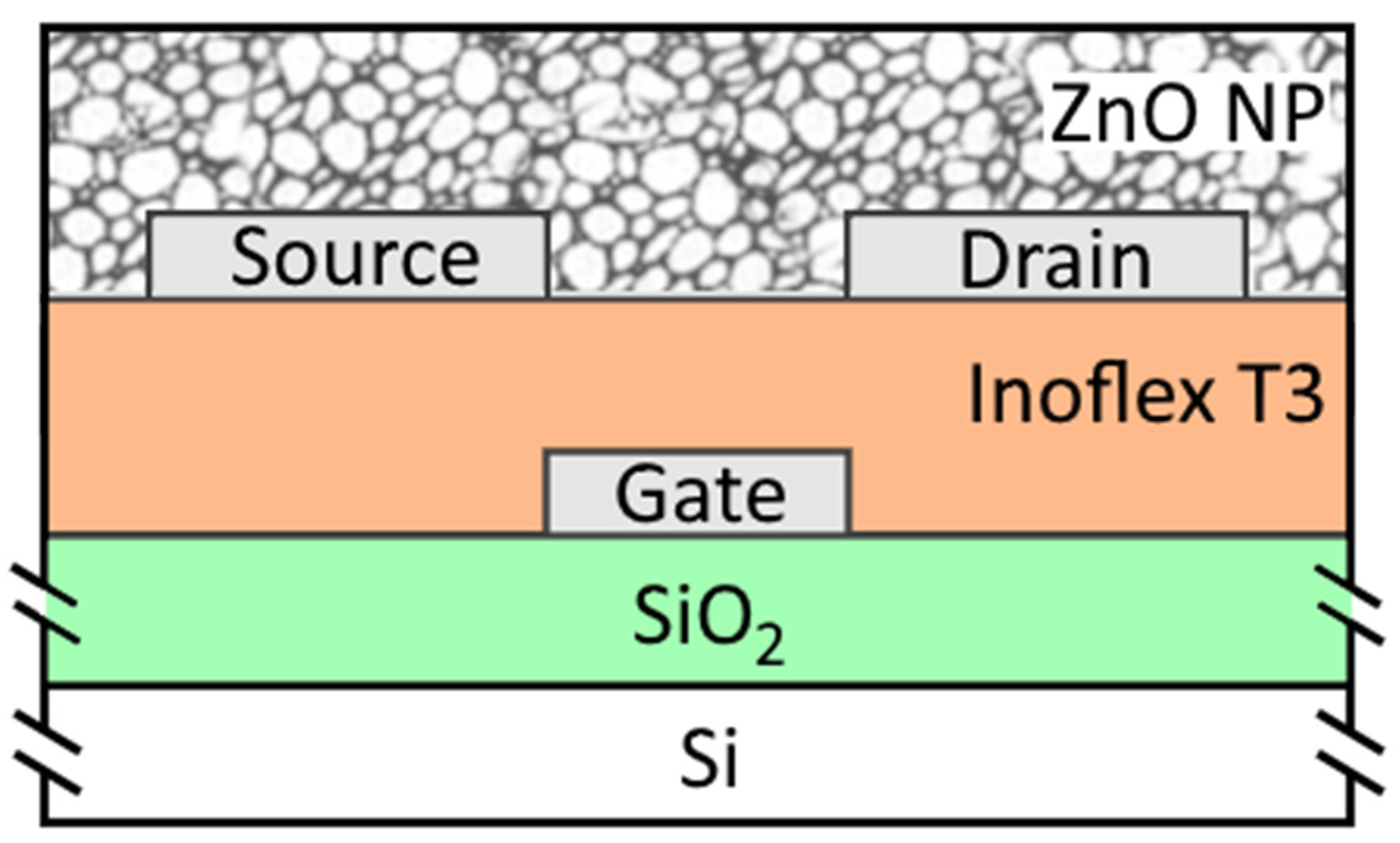
The TFTs were prepared over a SiO
2 (700 nm)/Si wafer with an inverted coplanar setup (
Figure 1). The wafer itself served as a rigid substrate for the present study purpose, although the TFT structures could be integrated on a transparent and flexible substrate in order to evaluate other parameters, like light transmittance and flexibility. In this manner, all the experiments were performed at the maximum temperature of 150 °C, simulating the thermal treatments for polymeric substrates. Over the SiO
2 layer, 50 nm of aluminum followed by 7 nm of titanium were evaporated under vacuum conditions. A gate pattern definition was performed using standard contact photolithography and wet etching processes. An organic-inorganic nanocomposite was used as a material for the gate dielectric (available from Inomat GmbH, trade name: Inoflex T3 [
11]), based on hydrolyzed and condensed acrylate functionalized silane. TiO
2 nanoparticles were added by co-condensation to increase the permittivity of the Inoflex T3 (ε
r = 10 at 50 Hz). The final thickness of the spin-coated gate dielectric was in the range of 150–180 nm. Thermal processes were also performed for cross-linking and curing in at 115 °C air temperature for 30 min followed by a UV exposure for a total of 4 min.
For the source and drain contacts, aluminum (Al), gold (Au), and nickel (Ni) were used (work function around 4.2 eV, 4.8 eV, and 4.9 eV, respectively) [
12]. These metals were evaporated and patterned following standard contact photolithography and lift-off processes, with thicknesses of 150 nm for Al and Ni, and 100 nm for Au. An aqueous ZnO NP dispersion was deposited over the TFTs template using the doctor blade technique [
13], forming a homogenous film covering the source and drain contacts and so filling the channel region. Moreover, a thermal process at an air temperature of 115 °C for 30 min was performed for water evaporation. A UV exposure of 4 min in total and a humidity treatment were also conducted in order to release O
2 molecules and adsorb H
2O molecules on the ZnO NP surface, increasing the film conductivity [
14]. For each set of metal, the channel length (source to drain distance) of 3 µm and 5 µm were considered, named L3 and L5, respectively. The width for both channel lengths was W = 1000 µm.
The TFTs were electrically characterized at room temperature in a dark and electrically isolated environment using a parameter analyzer Agilent 4156A.
3. TFT Electrical Parameters
The TFT performance usually can be evaluated in terms of some common electric parameters as µ
e, SS, V
on, V
th, and I
on/I
off. These parameters can be affected by the choice of gate dielectric and semiconductor materials and metals used for the gate and source/drain contacts. The metals chosen for source and drain terminals are especially highlighted in this study. These metals in contact with the ZnO NPs create an SBH that directly affects the TFT performance.
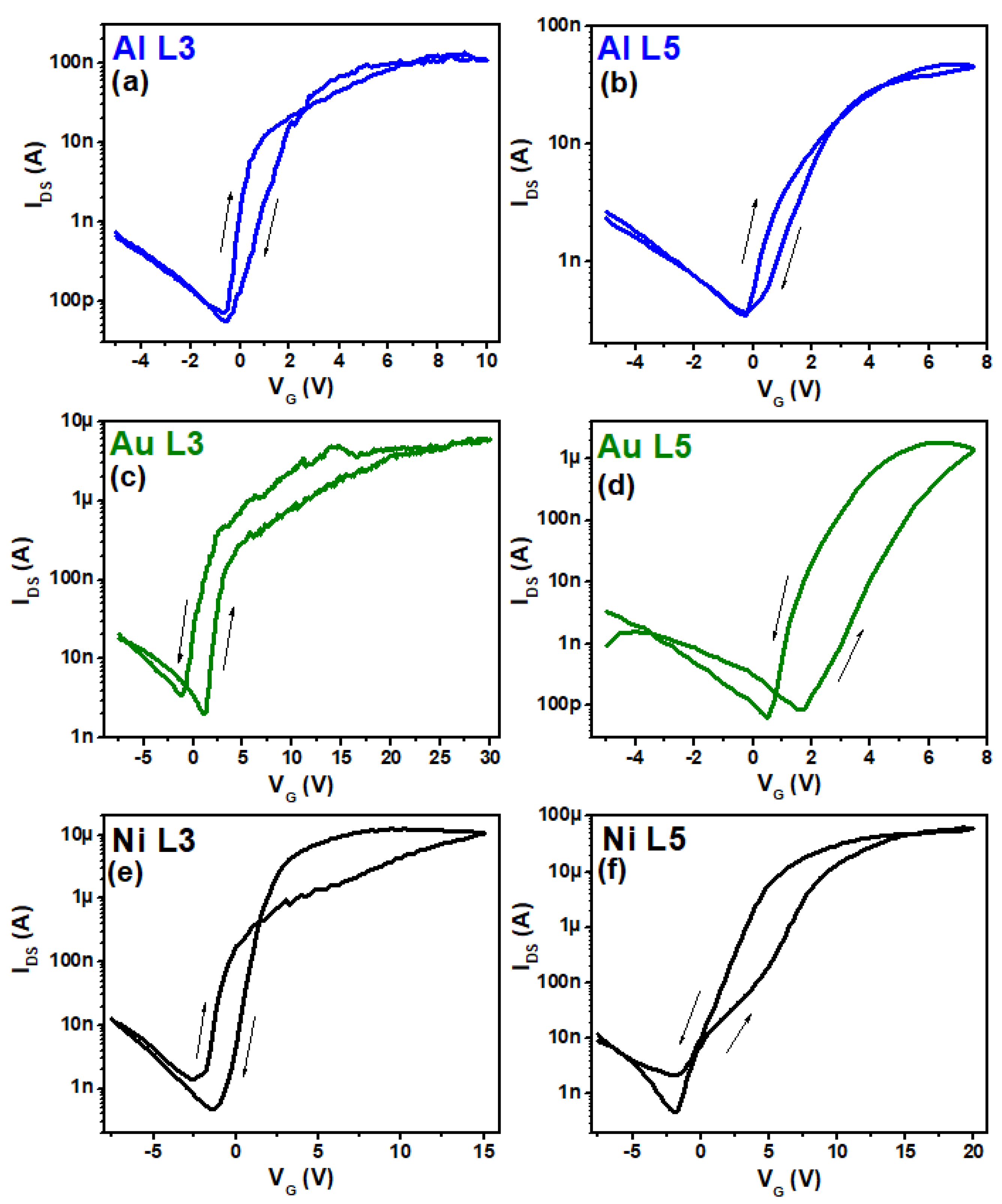
Figure 2 shows the transfer characteristic curves (I
DS vs. V
G) applying a source to drain voltage V
DS of 5 V for all the TFTs that were measured in this work. A summary of the results extracted from
Figure 2 are presented in
Table 1. For the extraction of the mobility, the transfer characteristics were necessary, from which the transconductance was obtained. Together with other parameters such as the dielectric capacitance, the length and width of the transistor’s channel, and the drain voltage, the value for the mobility could be evaluated. The Ni TFTs presented the best results. Ni L5 showed an I
on/I
off of 1.3 × 10
5 and mobility of 0.151 cm
2 V
−1 s
−1, despite the fact that it presented a higher SS and a more negative V
on voltage in comparison to the other TFTs. The Au TFTs showed intermediate results, being the only one with a positive V
on. The Al TFTs in this configuration did not have the expected characteristics, especially for I
on/I
off and mobility (the last one is in the range of 10
−4 cm
2 V
−1 s
−1). Specifically to the Al samples, it is well-known that the employment of inverted coplanar setup jeopardizes the contact area between the drain and source electrodes and the active semiconducting layer [
15,
16]. Additionally, the lift-off techniques used in the integration process could induce chemical stress at the dielectric-semiconductor interface [
17].
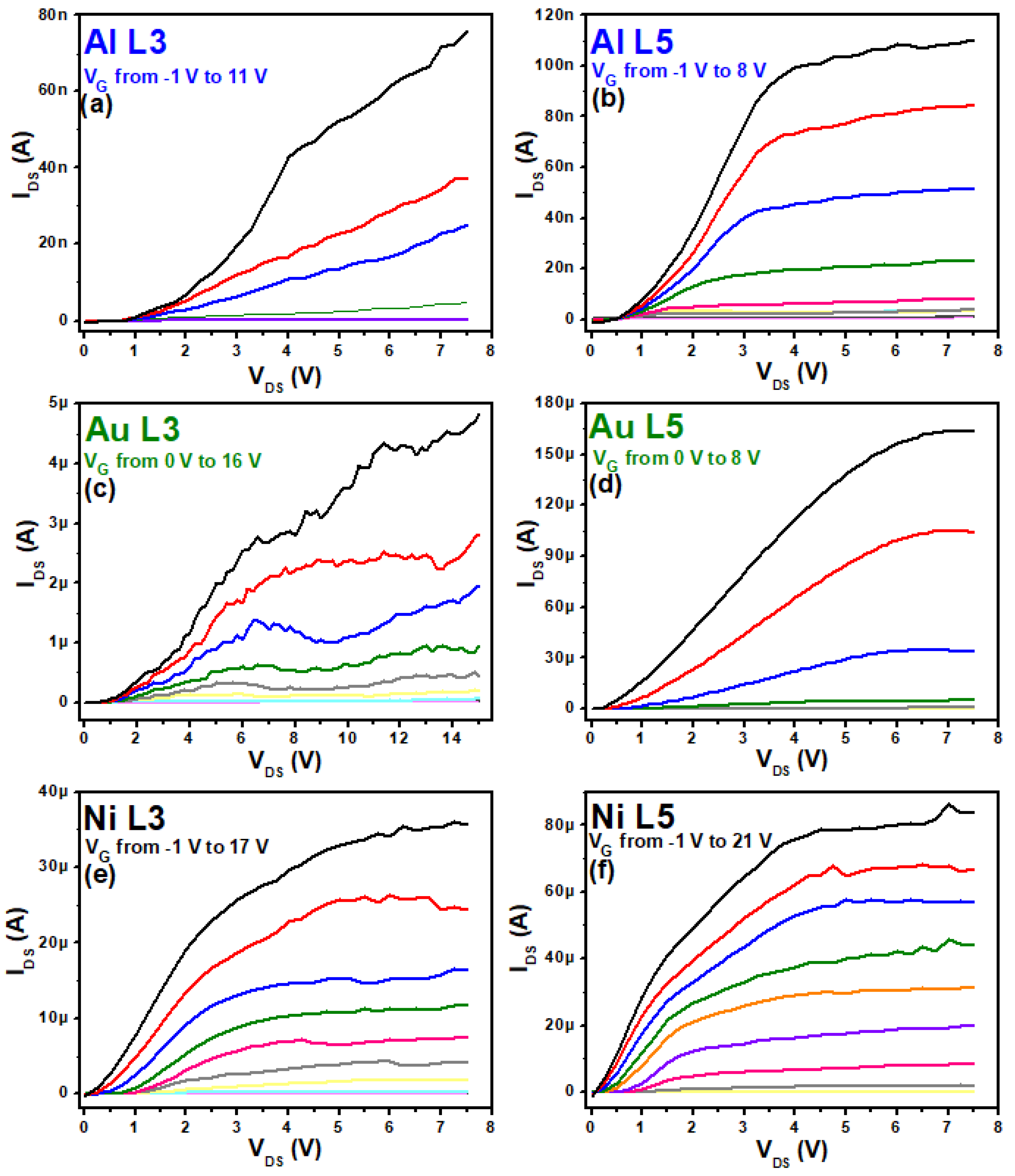
The output characteristic curves are shown in
Figure 3. The first noticeable aspect of these curves was that Ni TFTs presented a saturation current for higher V
DS in all the ranges of the gate voltage (V
G) applied, from depletion to strong accumulation (negative to positive V
G). In addition, the Ni TFTs depicted the highest channel current on accumulation mode. The Au transistors presented with an intermediate behavior, yet with no clear saturation current established. For a fixed V
G value of 8 V and in the saturation region of the L5 TFTs, the highest I
DS was for Ni (~5 µA), followed by Au (~0.6 µA) and Al (~0.1 µA). An s-shape was also observable for the Al and Au TFTs, indicating a high contact resistance between metal and semiconductor [
18].
From the previous analysis, TFTs with Ni source and drain metallization showed the best results, followed by Au and Al, respectively. The current injected from source/drain into the n-type channel plays an important role in better understanding TFTs behavior. For this reason, a more detailed study regarding the current in Metal-Semiconductor-Metal (MSM) structures is required [
10].
4. Metal-Semiconductor-Metal (MSM) Measurements
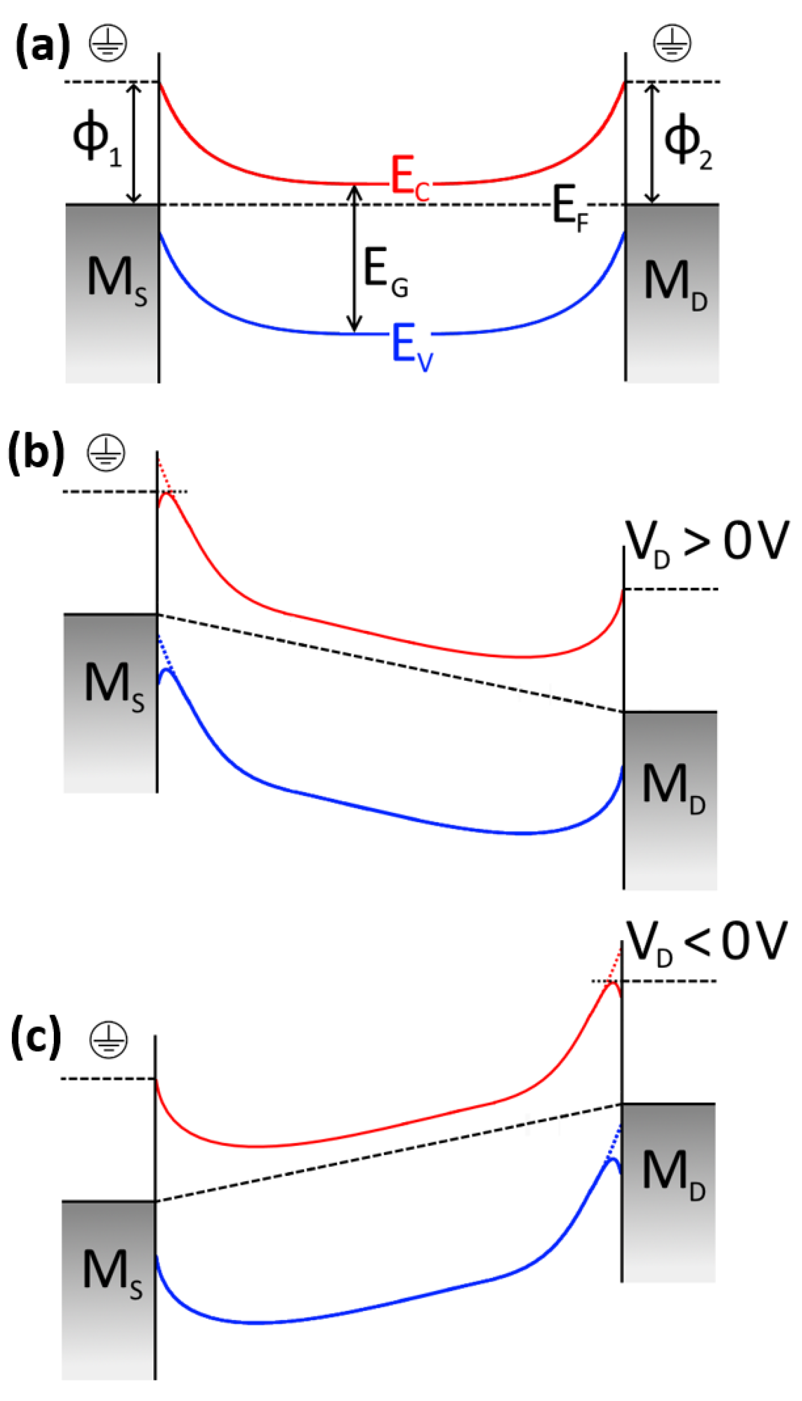
The electrical current in a TFT structure can be understood as a flow of negative charges going from one metal (drain) electrode into the channel and then being collected by the other metal (source) electrode. This means that in the TFTs, a Metal-Semiconductor-Metal (MSM) structure exists with one Schottky diode at each interface.
Figure 4a shows the band diagram with no voltage applied in the source (M
S) and drain (M
D) metals. When metal and semiconductors were in contact, the semiconductor Fermi level aligned with the metalwork function. A Schottky barrier appeared in each interface, and electrons faced this energy barrier when one of the diodes was reverse biased. In fact, what limits the current in TFTs is the diode that is reverse biased [
19].
Figure 4b,c illustrates the case when M
D has positive and negative voltages applied, respectively (note that M
S is ground potential). In
Figure 4b, the diode in the M
S interface was reverse biased, and the diode in the M
D interface was direct biased, and the contrary is presented in
Figure 4c. The equation that regulates the current I(V
DS) in TFTs can thus be written as in [
19,
20]:
where the saturation currents I
1 and I
2 are given by:
In the above-mentioned equations, k
B is the Boltzmann constant, T is the absolute temperature in Kelvin, S
1 and S
2 are the diodes areas (thickness vs. width) in cm
2, A* is the effective Richardson constant (A* = 32 A cm
−2 K
−2 for ZnO NP [
21]), Φ
1 and Φ
2 are the SBH in eV, n
1 and n
2 are the ideality factors for each diode junction and V
DS is the drain-to-source voltage difference. The ideality factor gives information about the current mechanism involved in the Schottky junction. An ideality factor close to unity means that all the current is generated by thermionic emission. Values above unity reveal that other current mechanisms are involved, like tunneling, recombination, and diffusion of electrons or holes [
22].
The gate voltage V
G can also regulate the total current in a TFT. In this case, the saturation currents I
1 and I
2 can be modulated depending on the V
G applied, and hence the total current is a function not only of V
DS, but also of V
G: I (V
DS, V
G) [
23].
As the total current in TFTs is limited by the diode that is reverse biased, it is important that the SBHs are as low or thin as possible, reproducing ohmic contacts in both Schottky junctions. Indeed, when the TFT is in the on state, it is essential that it conducts the maximum current possible with the lowest VDS bias applied. Still, the gate electrode takes control over the TFT between the on and off state, accumulating or depleting the channel and so modulating the operation.
For all the TFTs (Al, Au, and Ni, L = 3 and 5 µm) the output curves I
DS vs. V
DS with different V
G were measured, both in the positive and negative range of V
DS. Using Equations (1)–(3) it was possible to fit the model to all experimental data and to extract information about SBH and ideality factors for both diodes of each TFT.
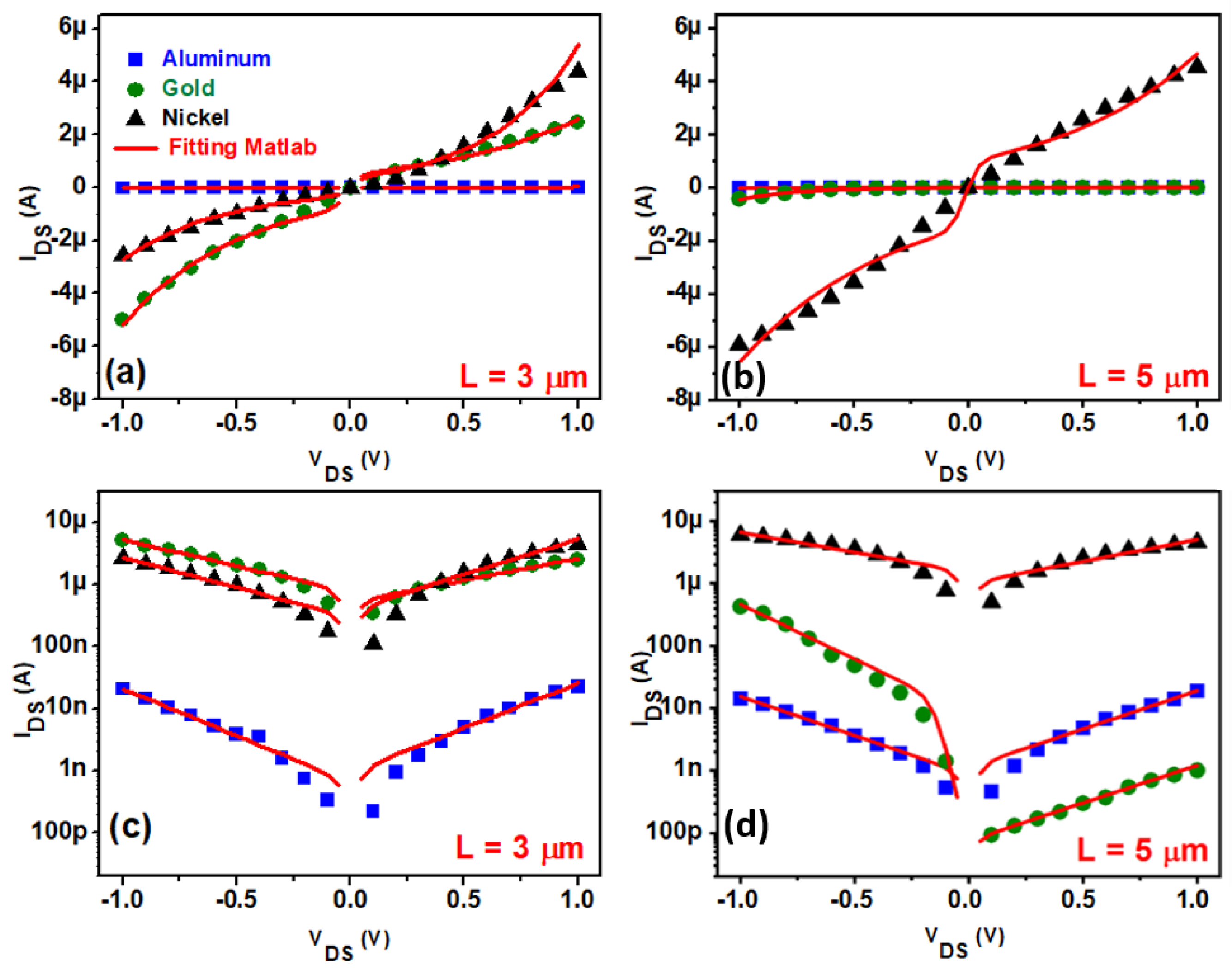
Figure 5a,b presents a plot of the experimental points and the simulation lines of I
DS vs. V
DS, with V
DS ranging from −1 to 1 V and V
G fixed at 4 V. For the fitting, the numerical computing software MATLAB (version R2018b) was used [
24]. For the sake of clarity,
Figure 5c,d depict the same results for Al L = 3 µm, Al L = 5 µm and Au L = 5 µm; however, in log scale for a better observation of the fitting curves. As can be seen, the fitting model was in good accuracy with the experimental points for all the source/drain metals used. A coefficient of determination R
2 around 0.97 ± 0.03 was evaluated for all simulations in this work.
Figure 5 shows that the Al TFTs presented the lowest current among the metals, which was around two orders of magnitude lower than for Ni TFTs. Ni and Au TFTs presented close current values for L = 3 µm, but the Ni transistor in L = 5 µm had a higher current for both positive and negative V
DS bias.
Although
Figure 5 presents the result for V
DS ranging from −1 to +1 V, we have also measured and implemented the fitting for the data of V
DS going from −2 to +2 V, −5 to +5 V, and −10 to +10 V. The SBHs and ideality factors were then extracted and plotted in
Figure 6 and
Figure 7. The Schottky barrier heights Φ
1 and Φ
2 were obtained by the saturation currents from the reverse diodes related to Equations (2) and (3), respectively. For the positive and negative V
DS range, information about Φ
1 and Φ
2 were obtained, respectively. The ideality factors, on the contrary, were mainly correlating with the direct bias diodes. In this way, n
1 was strongly correlated to the negative V
DS range and n
2 with the positive range.
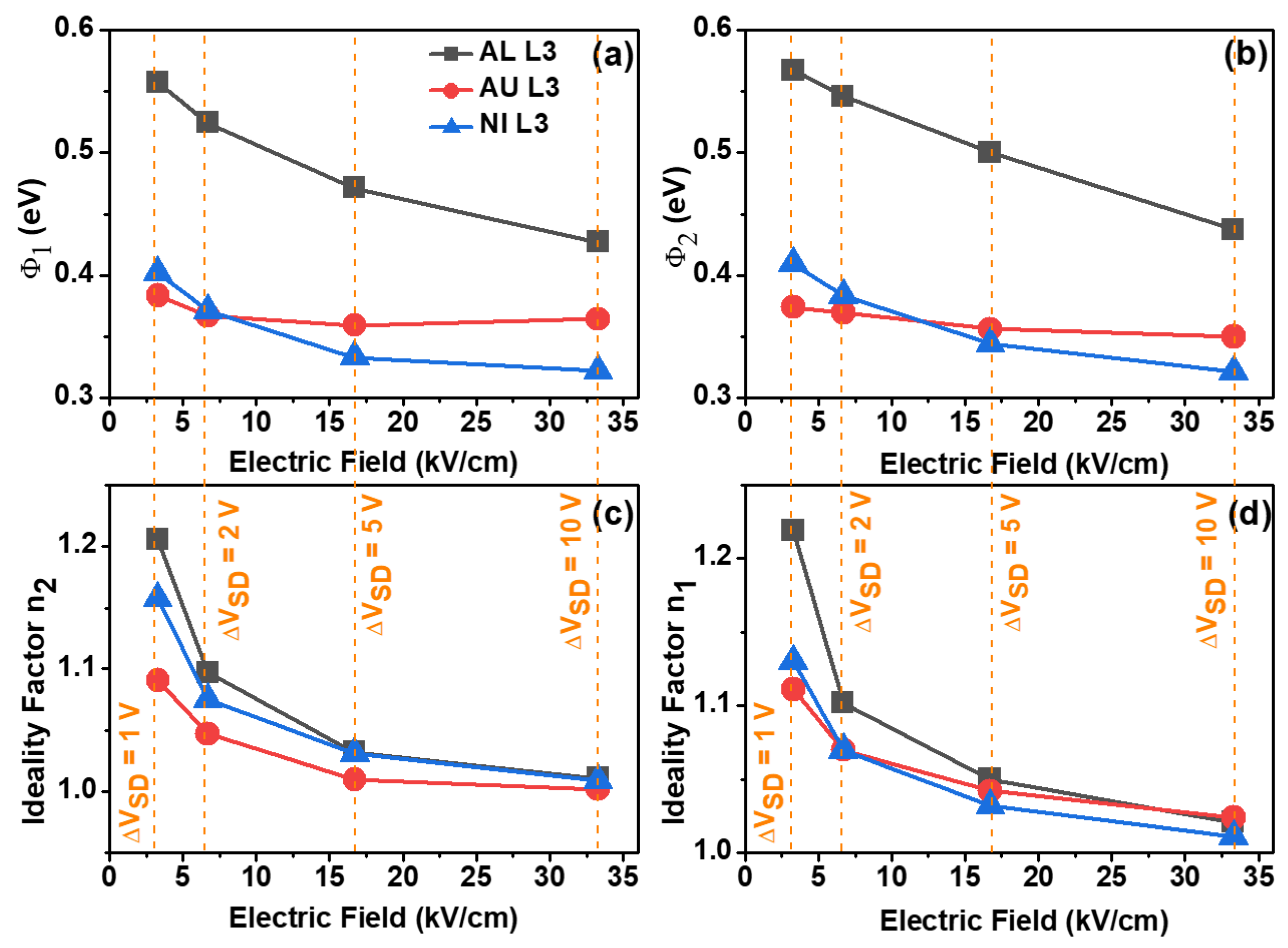
Figure 6 shows the results of the SBH and the ideality factors as a function of the electric field modulus created by the potential difference between source and drain (∆V
DS = 1, 2, 5, and 10 V) for TFTs with L = 3 µm. For these measurements, a fixed V
G of 4 V was applied. For both SBH, the Al transistor showed the highest values, ranging from 0.56 to 0.44 eV accordantly to the electric field increase. Au and Ni TFTs had closer SBH values, ranging from 0.40 to 0.34 eV. Yet, for the higher electric field, the Ni TFT presented with the lowest SBH of 0.32 eV.
The SBH decreasing with a higher electric field is well known as the Schottky effect (or image force lowering effect) [
25]. This effect is also represented in
Figure 4b,c, in the interface of the diode that was reverse biased, causing the conduction and valence bands to be curved. As the SBH at the reverse diode was decreased by the Schottky effect, it was also expected that the thermionic emission should be higher through the lowered SBH. The ideality factor should also decrease with increasing electric field. Indeed, this was what was observed in
Figure 6c,d. Even for the lowest ∆V
DS = 1 V, both ideality factors for all source/drain metals were n = 1.15 ± 0.05. As the electric field increased, both ideality factors were close to unity. In general, the ideality factor for the Al TFT was slightly higher than for Au and Ni (up to 0.1 higher with the smaller electric field).
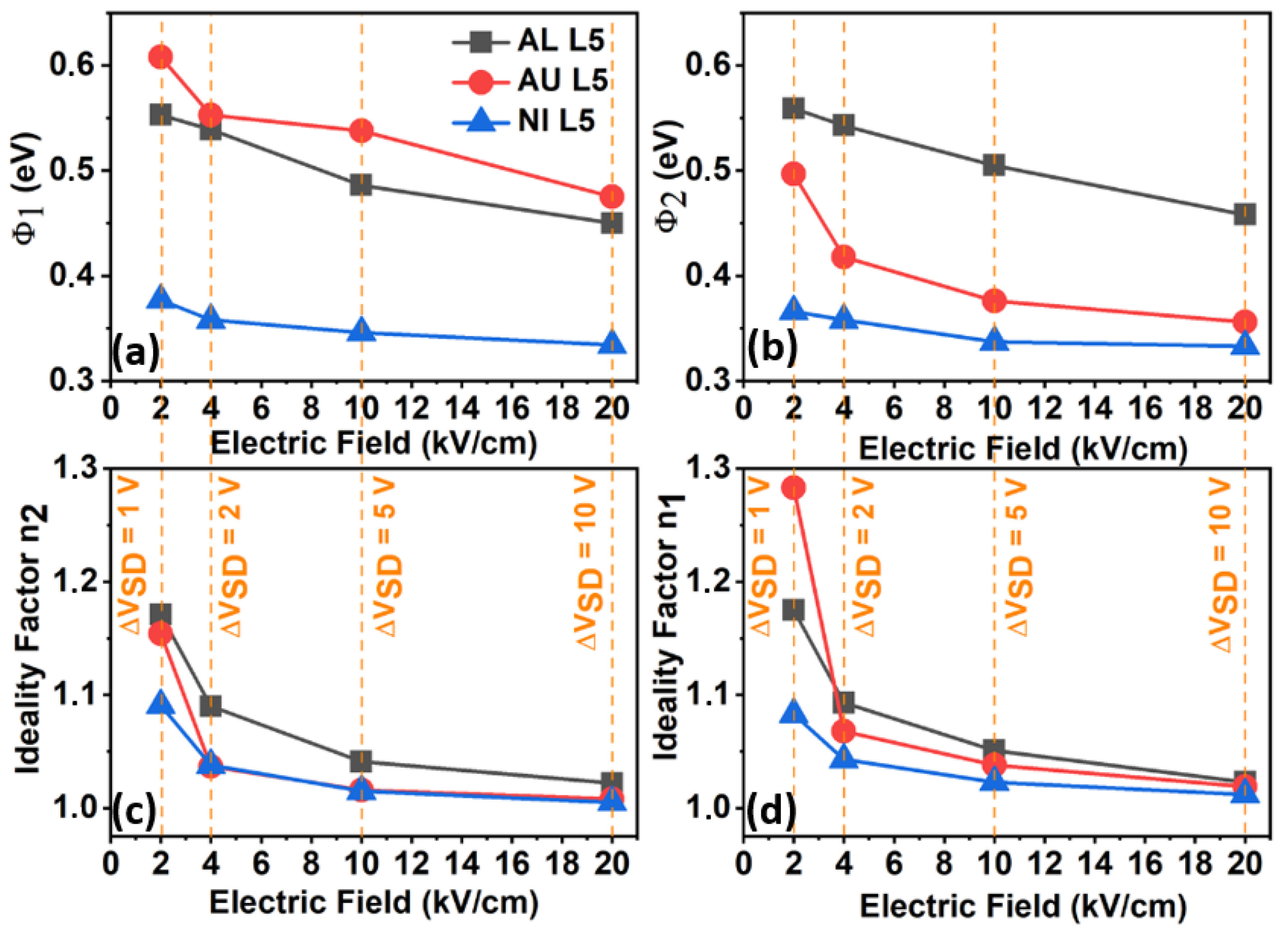
Figure 7 shows the results for the TFTs with L = 5 µm. The results for Al and Ni source/drain metals were in close agreement with the results presented in
Figure 6. For these samples, the channel length had no influence on the Schottky diodes. For Au L5, there was a significant difference between Φ
1 and Φ
2 and when compared to the results presented in
Figure 6b.
Figure 5d shows the logarithmic scale of I
DS vs. V
DS for the Au L = 5 µm TFT. In fact, the I
DS was not symmetric for the positive and negative V
DS range as it was for the other metals. Therefore, an asymmetry of the SBH was expected, as shown in
Figure 7. This asymmetry is still under investigation, and eventually, it might be found to be related to the memristor effect [
26,
27]. Even though the results of an inverted staggered TFTs setup are not presented in this work, this effect could also be observed in this kind of structurem, and it seems to be even more prominent.
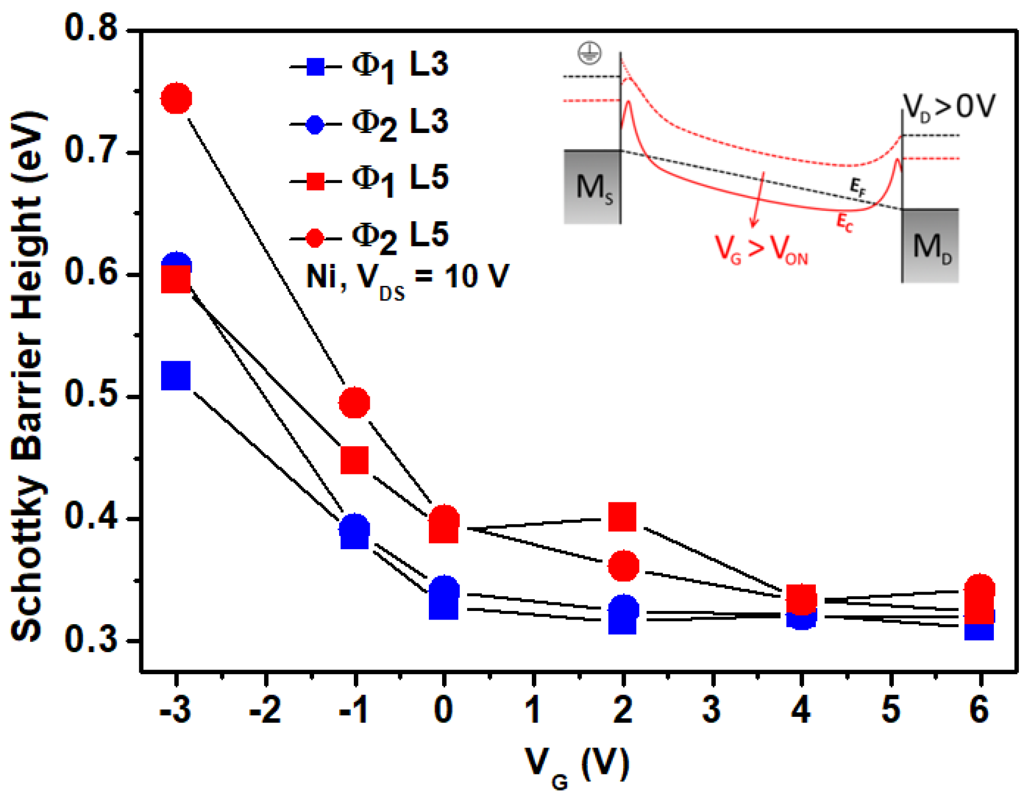
The Schottky effect also appears when the gate voltage V
G varies [
23].
Figure 8 shows the SBH as a functions of V
G for the Ni sample with V
DS = 10 V. Both the Φ
1 and Φ
2 of L = 3 and 5 µm are shown. As V
G increases for positive voltage, both SBHs decreased and tended to a value of around 0.32 eV. For the negative V
G, the channel was in depletion mode and presented a higher and non-convergent SBH value. The inset of
Figure 8 helps to elucidate this phenomenon. Not only did the drain-to-source voltage cause the Schottky effect to appear in the reverse diodes, but it also occurred when the gate voltage induced more electrons into the channel (for an n-type semiconductor). This effect was more prominent in both interfaces, independent of the diode being in the reverse or in the direct bias condition. With V
G > V
on, more electrons were induced into the channel, and the SBH width became thinner on both metal interfaces. Those electrons closer to the interface with the metals increasd the Schottky effect, causing the SBHs to be lowered with higher V
G [
23,
25].
With a high electric field in the channel or with a high V
G applied, it seems that for Ni source/drain metal; the SBH tended to a value close to ~0.3 eV. The Fermi-level pinning could fix the SBH to this value, but it is unclear if this is the case. A possible explanation might be that interface layers (like non-stoichiometry interfacial layers) cause the Fermi-level depinning [
28]. The work function of the metal surface can also be different from those known by a completely clean surface. In this matter, more measurements varying the temperature should be performed.
For a more precise Schottky analysis, the mathematical equations used for the Matlab simulation tool should also consider other charge transport mechanisms, especially tunneling through a possible thin insulator layer between metal and ZnO NP [
29] or traps at the metal/semiconductor interface and semiconductor bulk. As the barrier heights of metal/semiconductor systems are influenced by the metalwork function and by the interface states [
25], the current mechanism through traps could play an important role in the TFT channel current. Although previous studies addressing traps in ZnO NPs TFTs were performed by the authors [
14,
15,
30], how the interface states at the contacts and the presence of traps may influence the SBH, and thus the channel current remains an open question. Further studies regarding traps in TFTs are being carried out in order to have a better overall understanding of the charge carrier transport mechanism at these contacts, as well as in the semiconducting layer. Nevertheless, the model and the simulation tool proposed in this article describe in an accurate form the rule of the Schottky barriers and ideality factors in the charge transport mechanism that takes place in the interface of the MSM structures of the TFTs.


 ,
, 


