
Synthesis of Highly Conductive Electrospun Recycled Polyethylene Terephthalate Nanofibers Using the Electroless Deposition Method


 , , ,
, , ,  , and
, and 
Abstract
1. Introduction
2. Experimental Section
2.1. Materials
2.2. Fabrication of r-PET Nanofibers
2.3. Fabrication of Conductive r-PET Nanofibers
2.3.1. Plasma Treatment
2.3.2. Silanization
2.3.3. Polymerization
2.3.4. Electroless Deposition
2.4. SEM Morphology
2.5. XPS Analysis
2.6. Water Contact Angle
2.7. Tensile Strength Properties
2.8. Shrinkage Test
3. Results and Discussion
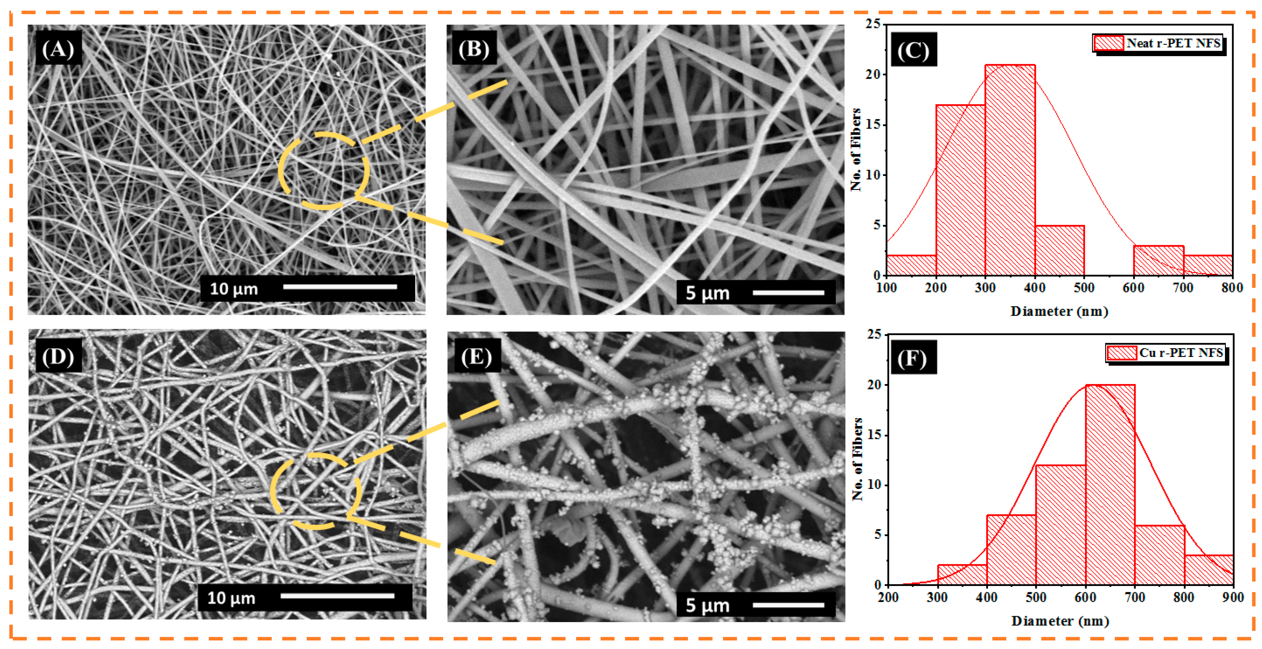
3.1. Scanning Electron Microscopy
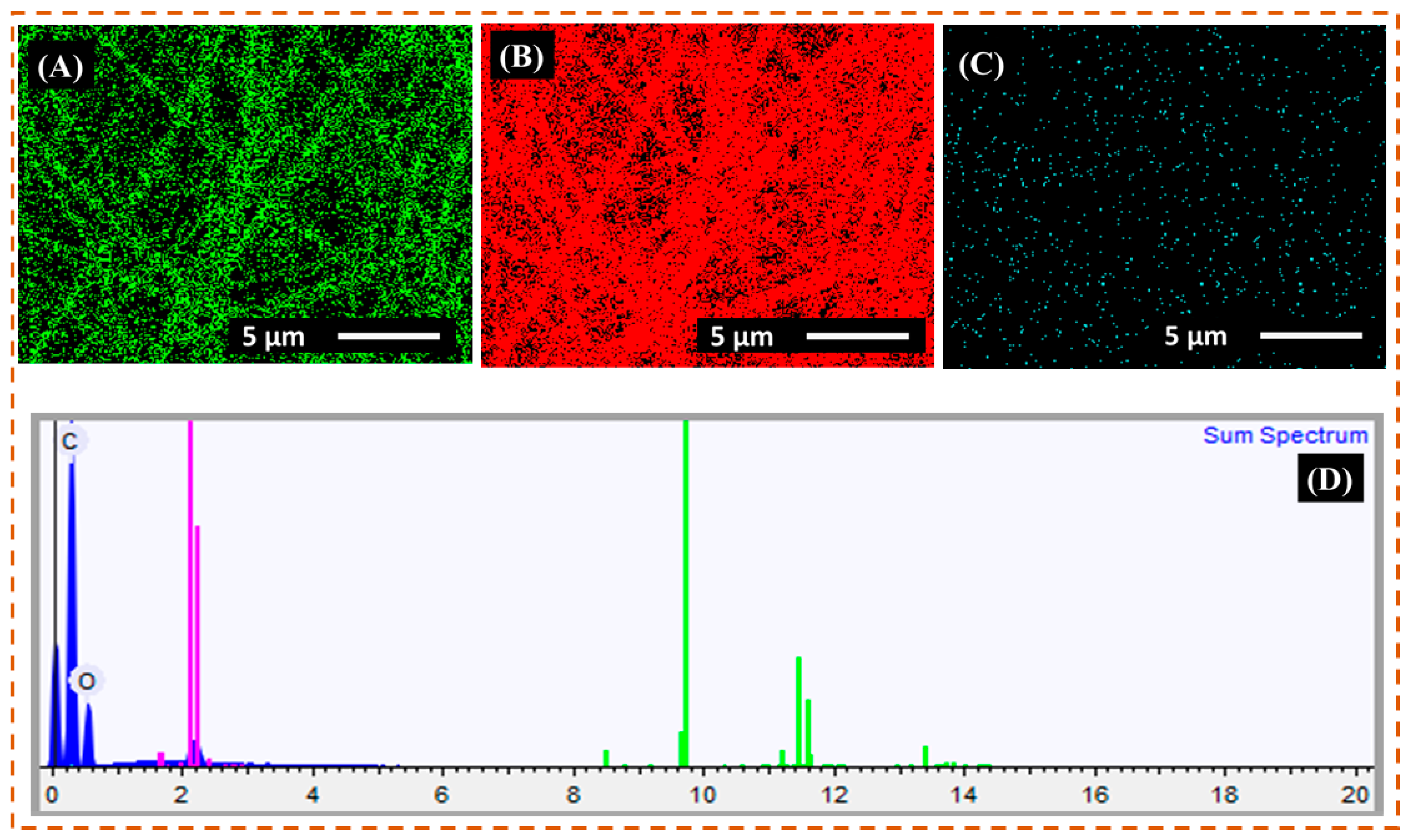
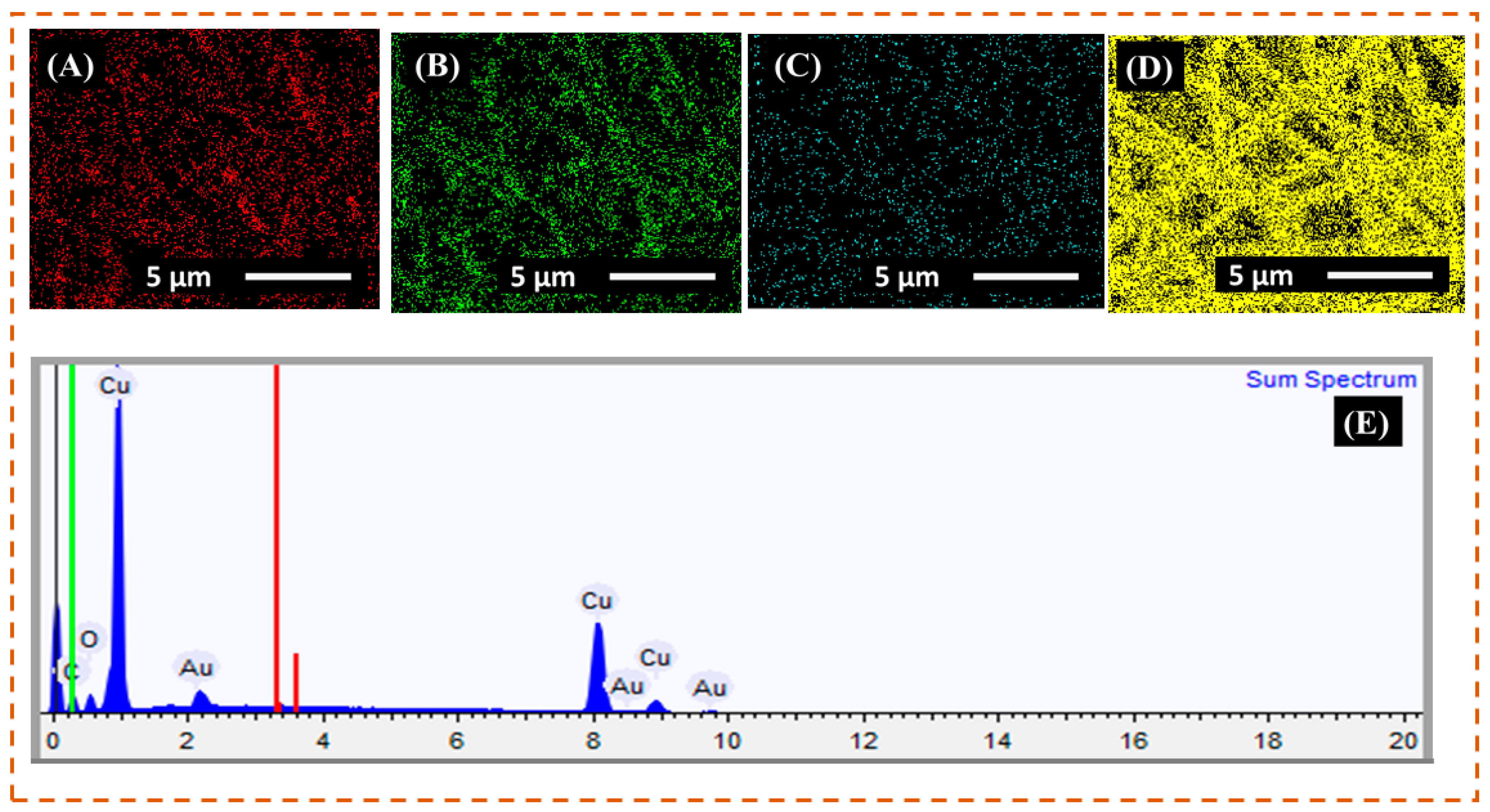
3.2. EDX Analysis
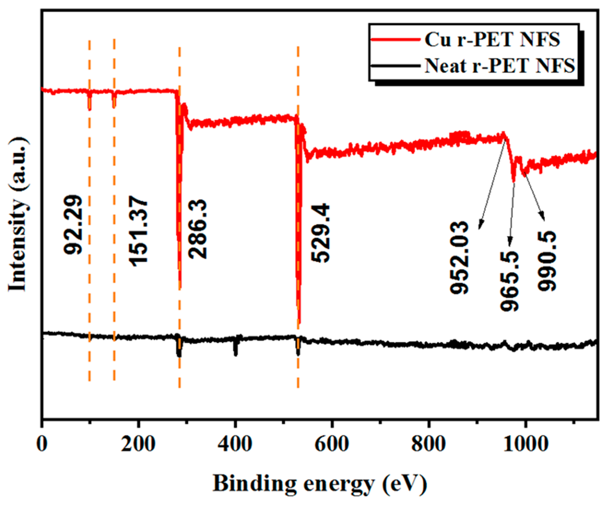
3.3. XPS Analysis
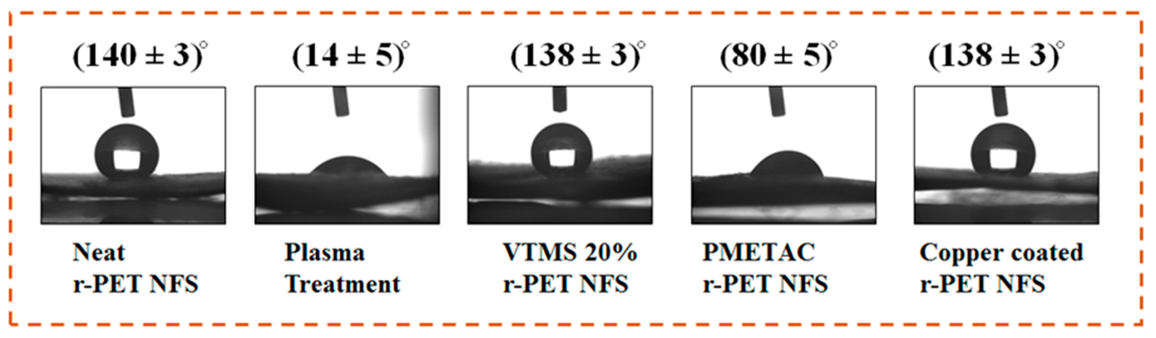
3.4. Water Contact Angle Analysis
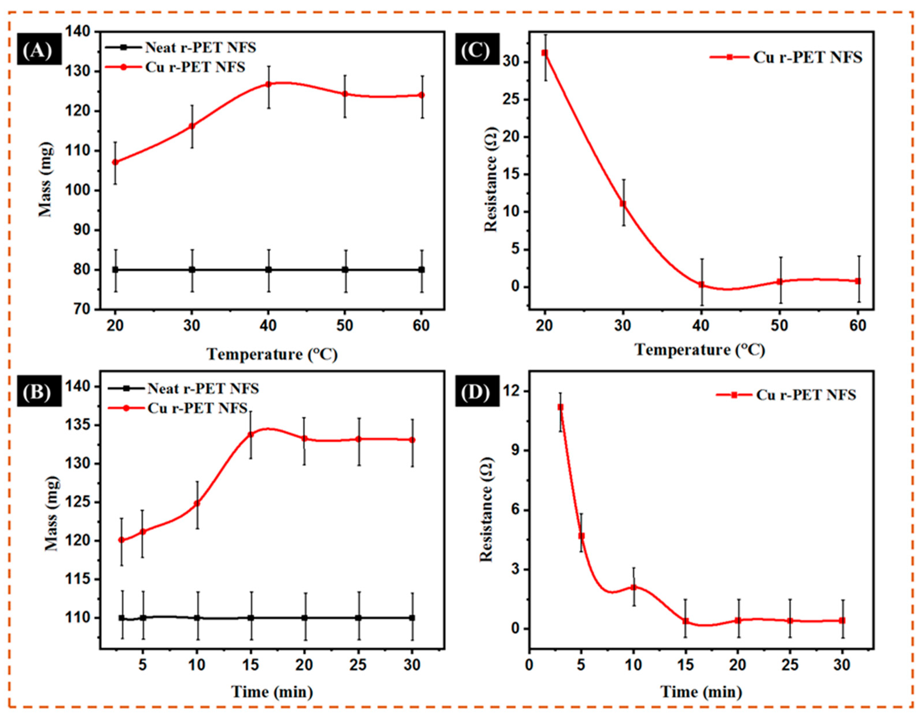
3.5. Optimum Temperature and Time Study
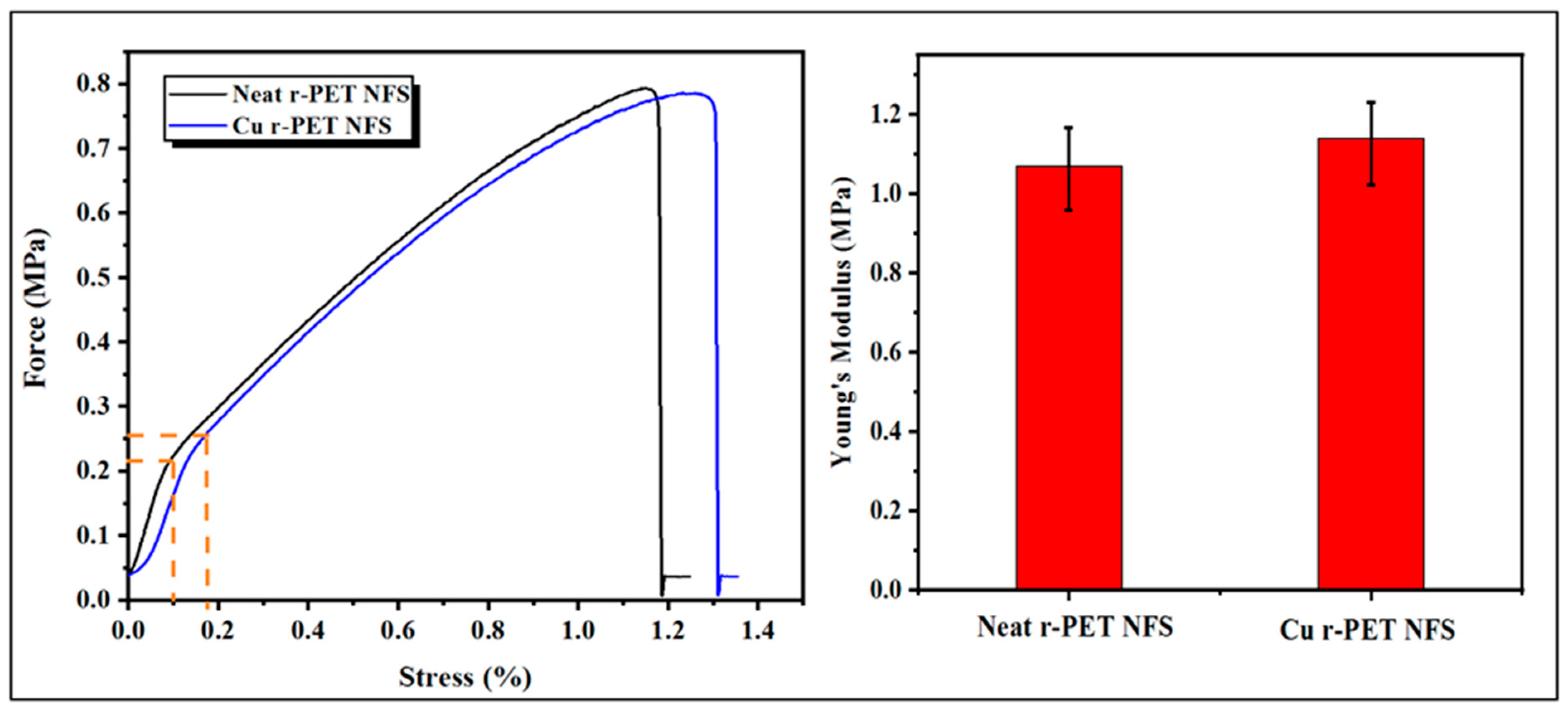
3.6. Tensile Strength
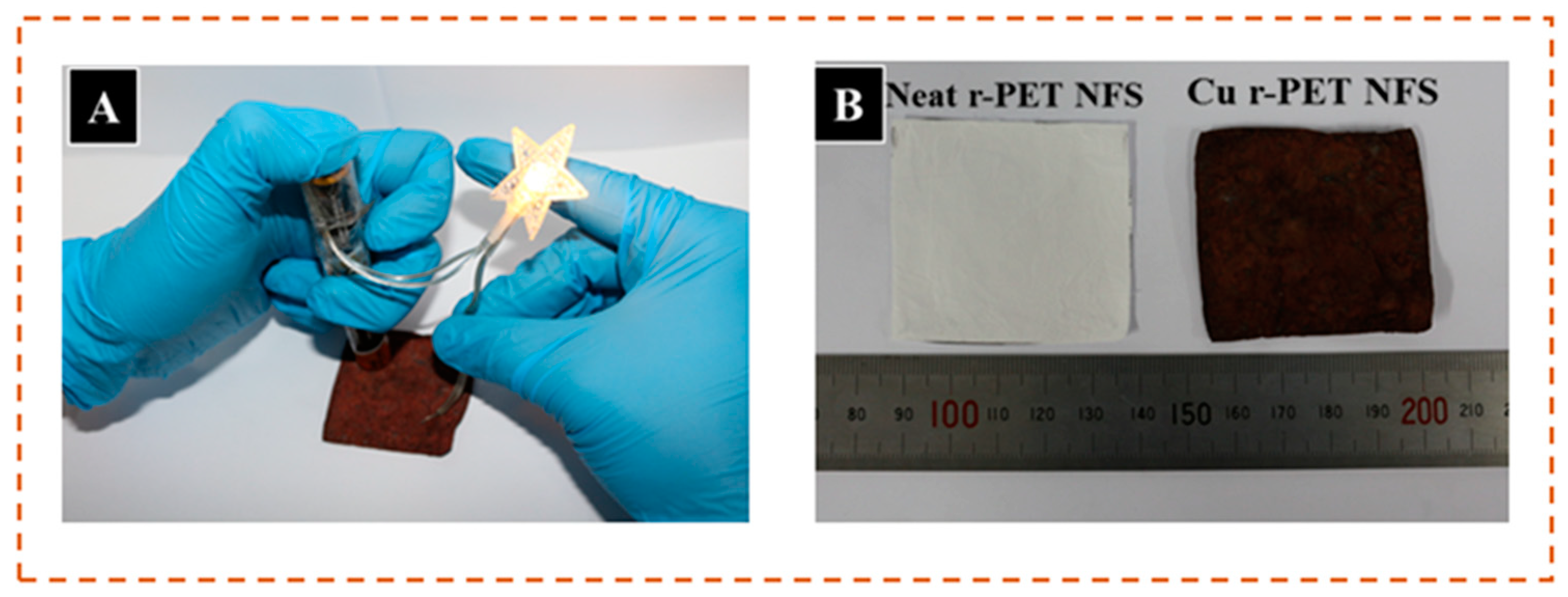
3.7. Shrinkage Study
4. Conclusions
Author Contributions
Funding
Institutional Review Board Statement
Informed Consent Statement
Data Availability Statement
Conflicts of Interest
References
- Wang, X.; Yan, C.; Hu, H.; Zhou, X.; Guo, R.; Liu, X.; Xie, Z.; Huang, Z.; Zheng, Z. Aqueous and air-compatible fabrication of high-performance conductive textiles. Chem. Asian J. 2014, 9, 2170–2177. [Google Scholar] [CrossRef]
- Hussain, N.; Yousif, M.; Ali, A.; Mehdi, M.; Ullah, S.; Ullah, A.; Mahar, F.K.; Kim, I.S. A facile approach to synthesize highly conductive electrospun aramid nanofibers via electroless deposition. Mater. Chem. Phys. 2020, 255, 123614. [Google Scholar] [CrossRef]
- White, M.S.; Kaltenbrunner, M.; Głowacki, E.D.; Gutnichenko, K.; Kettlgruber, G.; Graz, I.; Aazou, S.; Ulbricht, C.; Egbe, D.A.M.; Miron, M.C.; et al. Ultrathin, highly flexible and stretchable PLEDs. Nat. Photonics 2013, 7, 811–816. [Google Scholar] [CrossRef]
- Verpoorten, E.; Massaglia, G.; Ciardelli, G.; Pirri, C.F.; Quaglio, M. Design and optimization of piezoresistive peo/pedot:Pss electrospun nanofibers for wearable flex sensors. Nanomaterials 2020, 10, 2166. [Google Scholar] [CrossRef]
- Cui, J.; Zhou, Z.; Jia, M.; Chen, X.; Shi, C.; Zhao, N.; Guo, X. Solid polymer electrolytes with flexible framework of SiO2 nanofibers for highly safe solid lithium batteries. Polymers 2020, 12, 1324. [Google Scholar] [CrossRef]
- Benight, S.J.; Wang, C.; Tok, J.B.H.; Bao, Z. Stretchable and self-healing polymers and devices for electronic skin. Prog. Polym. Sci. 2013, 38, 1961–1977. [Google Scholar] [CrossRef]
- Mokhtari, F.; Shamshirsaz, M.; Latifi, M.; Foroughi, J. Nanofibers-based piezoelectric energy harvester for self-powered wearable technologies. Polymers 2020, 12, 2697. [Google Scholar] [CrossRef] [PubMed]
- Hu, L.; Pasta, M.; La Mantia, F.; Cui, L.; Jeong, S.; Deshazer, H.D.; Choi, J.W.; Han, S.M.; Cui, Y. Stretchable, porous, and conductive energy textiles. Nano Lett. 2010, 10, 708–714. [Google Scholar] [CrossRef]
- Pandey, P.A.; Bell, G.R.; Rourke, J.P.; Sanchez, A.M.; Elkin, M.D.; Hickey, B.J.; Wilson, N.R. Physical vapor deposition of metal nanoparticles on chemically modified graphene: Observations on metal-graphene interactions. Small 2011, 7, 3202–3210. [Google Scholar] [CrossRef] [PubMed]
- Grodzicki, A.; Łakomska, I.; Piszczek, P.; Szymańska, I.; Szłyk, E. Copper(I), silver(I) and gold(I) carboxylate complexes as precursors in chemical vapour deposition of thin metallic films. Coord. Chem. Rev. 2005, 249, 2232–2258. [Google Scholar] [CrossRef]
- Myndrul, V.; Vysloužilová, L.; Klápšt’Ová, A.; Coy, E.; Jancelewicz, M.; Iatsunskyi, I. Formation and photoluminescence properties of ZnO nanoparticles on electrospun nanofibers produced by atomic layer deposition. Coatings 2020, 10, 1199. [Google Scholar] [CrossRef]
- Leary, J.D.; Hamouda, F.; Mazé, B.; Pourdeyhimi, B. Preparation of pseudocapacitor electrodes via electrodeposition of polyaniline on nonwoven carbon fiber fabrics. J. Appl. Polym. Sci. 2016, 133, 1–8. [Google Scholar] [CrossRef]
- Azzaroni, O.; Zheng, Z.; Yang, Z.; Huck, W.T.S. Polyelectrolyte brushes as efficient ultrathin platforms for site-selective copper electroless deposition. Langmuir 2006, 22, 6730–6733. [Google Scholar] [CrossRef]
- Yu, Y.; Yan, C.; Zheng, Z. Polymer-assisted metal deposition (PAMD): A full-solution strategy for flexible, stretchable, compressible, and wearable metal conductors. Adv. Mater. 2014, 26, 5508–5516. [Google Scholar] [CrossRef] [PubMed]
- Garcia, A.; Polesel-Maris, J.; Viel, P.; Palacin, S.; Berthelot, T. Localized ligand induced electroless plating (LIEP) process for the fabrication of copper patterns onto flexible polymer substrates. Adv. Funct. Mater. 2011, 21, 2096–2102. [Google Scholar] [CrossRef]
- Liu, X.; Chang, H.; Li, Y.; Huck, W.T.S.; Zheng, Z. Polyelectrolyte-bridged metal/cotton hierarchical structures for highly durable conductive yarns. ACS Appl. Mater. Interfaces 2010, 2, 529–535. [Google Scholar] [CrossRef] [PubMed]
- Irfan, M.S.; Gill, Y.Q.; Hashmi, M.; Ullah, S.; Saeed, F.; Qaiser, A.A. Long-term stress relaxation behavior of Polyaniline-EPDM blends using the time-temperature-strain superposition method. Mater. Res. Express 2018, 6, 025318. [Google Scholar] [CrossRef]
- Irfan, M.S.; Gill, Y.Q.; Ullah, S.; Naeem, M.T.; Saeed, F.; Hashmi, M. Polyaniline-NBR blends by in situ polymerization: Application as stretchable strain sensors. Smart Mater. Struct. 2019, 28, 095024. [Google Scholar] [CrossRef]
- Huang, X.; Dai, B.; Ren, Y.; Xu, J.; Zhu, P. Preparation and study of electromagnetic interference shielding materials comprised of Ni-Co coated on web-like biocarbon nanofibers via electroless deposition. J. Nanomater. 2015. [Google Scholar] [CrossRef]
- Liu, S.; Hu, M.; Yang, J. A facile way of fabricating a flexible and conductive cotton fabric. J. Mater. Chem. C 2016, 4, 1320–1325. [Google Scholar] [CrossRef]
- Mu, S.; Xie, H.; Wang, W.; Yu, D. Electroless silver plating on PET fabric initiated by in situ reduction of polyaniline. Appl. Surf. Sci. 2015, 353, 608–614. [Google Scholar] [CrossRef]
- Yu, D.; Mu, S.; Liu, L.; Wang, W. Preparation of electroless silver plating on aramid fiber with good conductivity and adhesion strength. Colloids Surf. Physicochem. Eng. Asp. 2015, 483, 53–59. [Google Scholar] [CrossRef]
- Pang, H.; Bai, R.; Shao, Q.; Gao, Y.; Li, A.; Tang, Z. A novel Ag catalyzation process using swelling impregnation method for electroless Ni deposition on Kevlar ® fiber. Appl. Surf. Sci. 2015, 359, 280–287. [Google Scholar] [CrossRef]
- Mahar, F.K.; Mehdi, M.; Qureshi, U.A.; Brohi, K.M.; Zahid, B.; Ahmed, F.; Khatri, Z. Dyeability of recycled electrospun polyethylene terephthalate (PET) nanofibers: Kinetics and thermodynamic study. J. Mol. Liq. 2017, 248, 911–919. [Google Scholar] [CrossRef]
- Bohaczuk Venturelli, R.; Serafini Immich, A.P.; MA Guelli U de Souza, S.; U de Souza, A.A. Recycled polyester nanofiber as a reservoir for essential oil release. J. Appl. Polym. Sci. 2020, 50258. [Google Scholar] [CrossRef]
- Hashmi, M.; Ullah, S.; Ullah, A.; Akmal, M.; Saito, Y.; Hussain, N.; Ren, X.; Kim, I.S. Optimized Loading of Carboxymethyl Cellulose (CMC) in Tri-component Electrospun Nanofibers Having Uniform Morphology. Polymer 2020, 12, 2524. [Google Scholar] [CrossRef]
- Nadir, H.; Sana, U.; Muhammad, N.S.; Motahira, H.; Muzamil, K.; Takumi, Y.; Zeeshan, K.; Ick, S.K. Fabrication and Characterization of Novel Antibacterial Ultrafine Nylon-6 Nanofibers Impregnated by Garlic Sour. Fibers Polym. 2020, 21, 2780–2787. [Google Scholar] [CrossRef]
- Ullah, S.; Hashmi, M.; Hussain, N.; Ullah, A.; Sarwar, M.N.; Saito, Y.; Kim, S.H.; Kim, I.S. Stabilized nanofibers of polyvinyl alcohol (PVA) crosslinked by unique method for efficient removal of heavy metal ions. J. Water Process. Eng. 2020, 33, 101111. [Google Scholar] [CrossRef]
- Mehdi, M.; Mahar, F.K.; Qureshi, U.A.; Khatri, M.; Khatri, Z.; Ahmed, F.; Kim, I.S. Preparation of colored recycled polyethylene terephthalate nanofibers from waste bottles: Physicochemical studies. Adv. Polymer Technol. 2018, 37, 2820–2827. [Google Scholar] [CrossRef]
- Wang, B.; Zhao, M.; Mehdi, M.; Wang, G.; Gao, P.; Zhang, K.Q. Biomolecule-assisted synthesis and functionality of metal nanoclusters for biological sensing: A review. Mater. Chem. Front. 2019, 3, 1722–1735. [Google Scholar] [CrossRef]
- Hashmi, M.; Ullah, S.; Ullah, A.; Khan, M.Q.; Hussain, N.; Khatri, M.; Bie, X.; Lee, J.; Kim, I.S. An optimistic approach “from hydrophobic to super hydrophilic nanofibers” for enhanced absorption properties. Polym. Test. 2020, 90, 106683. [Google Scholar] [CrossRef]
- Hashmi, M.; Ullah, S.; Kim, I.S. Electrospun Momordica Charantia Incorporated Polyvinyl Alcohol (PVA) Nanofibers for Antibacterial Applications. Mater. Today Commun. 2020, 101161. [Google Scholar] [CrossRef]
- Sereshti, H.; Amini, F.; Najarzadekan, H. Electrospun polyethylene terephthalate (PET) nanofibers as a new adsorbent for micro-solid phase extraction of chromium(VI) in enVIronmental water samples. RSC Adv. 2015, 5, 89195–89203. [Google Scholar] [CrossRef]
- Guo, R.H.; Jiang, S.X.; Yuen, C.W.M.; Ng, M.C.F.; Lan, J.W. Optimization of electroless nickel plating on polyester fabric. Fibers Polym. 2013, 14, 459–464. [Google Scholar] [CrossRef]
- Demir, A.; Bozaci, E.; Gülümser, T.; Sarikanat, M. An ecological approach for the surface modification of aramid fibers. Tekst. Konfeksiyon 2016, 26, 256–261. [Google Scholar]
- Wang, C.; Yang, H.; Chen, F.; Peng, L.; Gao, H.-F.; Zhao, L.-P. Influences of VTMS/SiO2 ratios on the contact angle and morphology of modified super-hydrophobic silicon dioxide material by vinyl trimethoxy silane. Results Phys. 2018, 10, 891–902. [Google Scholar] [CrossRef]
- Politakos, N.; Azinas, S.; Moya, S.E. Responsive Copolymer Brushes of Poly[(2-(Methacryloyloxy)Ethyl) Trimethylammonium Chloride] (PMETAC) and Poly(1H,1H,2H,2H-Perfluorodecyl acrylate) (PPFDA) to Modulate Surface Wetting Properties. Macromol. Rapid Commun. 2016, 37, 662–667. [Google Scholar] [CrossRef]
- Tai, Y.; Xu, C.; Chen, H. Silver-coated glass fabric composites prepared by electroless plating. Mater. Lett. 2016, 180, 144–147. [Google Scholar] [CrossRef]


| Gas | Pressure (Pa) | Power (W) | Time (min) |
|---|---|---|---|
| Oxygen | 30 | 45 | 5 |
| Chemicals | Formula | Process | Concentration |
|---|---|---|---|
| VTMS | C5H12O3Si | Salinization | 20% (v/v in ethanol) |
| METAC | C9H18ClNO2 | Polymerization | 20% |
| Potassium persulfate | K2S2O8 | Ion Exchanger | 60 mg/100 mL |
| Ammonium tetrachloropalladate(II) | (NH4)2PdCl4 | 5 mM |
| Chemicals | Formula | Concentration | |
|---|---|---|---|
| Solution A | Potassium sodium tartrate | KNaC4H4O6·4H2O | 29 g/L |
| tetrahydrate | NaOH | 12 g/L | |
| Sodium hydroxide | |||
| Solution B | Copper(II) sulfate pentahydrate | CuSO4·5H2O | 13 g/L |
| Formaldehyde | HCHO | 9.5 g/L |
| Element | Weight% | Weight% σ | Atomic% |
|---|---|---|---|
| Carbon | 66.649 | 0.286 | 72.692 |
| Oxygen | 33.351 | 0.286 | 27.308 |
| Element | Weight% | Weight% σ | Atomic% |
|---|---|---|---|
| Carbon | 16.098 | 0.352 | 46.818 |
| Oxygen | 5.786 | 0.158 | 12.633 |
| Copper | 71.685 | 0.379 | 39.409 |
| Gold | 6.430 | 0.242 | 1.140 |
| Shrinkage a | Lengthwise | Widthwise |
|---|---|---|
| Cu r-PET NFS | 11% | 12% |
Publisher’s Note: MDPI stays neutral with regard to jurisdictional claims in published maps and institutional affiliations. |
© 2021 by the authors. Licensee MDPI, Basel, Switzerland. This article is an open access article distributed under the terms and conditions of the Creative Commons Attribution (CC BY) license (http://creativecommons.org/licenses/by/4.0/).
Share and Cite
Hussain, N.; Mehdi, M.; Yousif, M.; Ali, A.; Ullah, S.; Hussain Siyal, S.; Hussain, T.; Kim, I.S. Synthesis of Highly Conductive Electrospun Recycled Polyethylene Terephthalate Nanofibers Using the Electroless Deposition Method. Nanomaterials 2021, 11, 531. https://doi.org/10.3390/nano11020531
Hussain N, Mehdi M, Yousif M, Ali A, Ullah S, Hussain Siyal S, Hussain T, Kim IS. Synthesis of Highly Conductive Electrospun Recycled Polyethylene Terephthalate Nanofibers Using the Electroless Deposition Method. Nanomaterials. 2021; 11(2):531. https://doi.org/10.3390/nano11020531
Chicago/Turabian StyleHussain, Nadir, Mujahid Mehdi, Muhammad Yousif, Aizaz Ali, Sana Ullah, Sajid Hussain Siyal, Tanweer Hussain, and Ick Soo Kim. 2021. "Synthesis of Highly Conductive Electrospun Recycled Polyethylene Terephthalate Nanofibers Using the Electroless Deposition Method" Nanomaterials 11, no. 2: 531. https://doi.org/10.3390/nano11020531
APA StyleHussain, N., Mehdi, M., Yousif, M., Ali, A., Ullah, S., Hussain Siyal, S., Hussain, T., & Kim, I. S. (2021). Synthesis of Highly Conductive Electrospun Recycled Polyethylene Terephthalate Nanofibers Using the Electroless Deposition Method. Nanomaterials, 11(2), 531. https://doi.org/10.3390/nano11020531