
Highly Efficient Near-Infrared Detector Based on Optically Resonant Dielectric Nanodisks


 and
and 
Abstract
1. Introduction
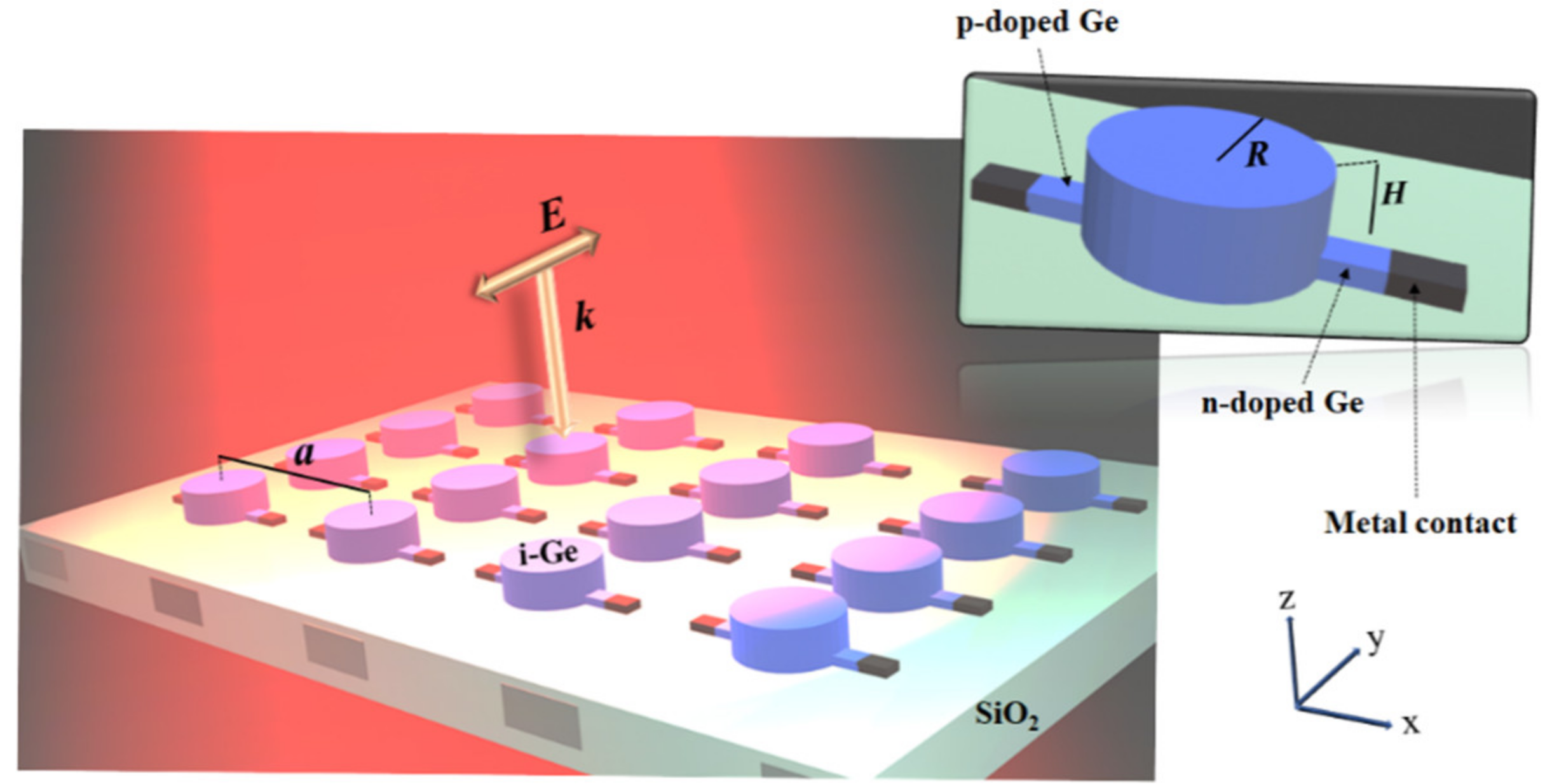
2. Device Configuration
3. Device Performance

| Structure | Highest Responsivity (A/W) | Dark Current | Highest 3 dB Bandwidth | Year | Ref |
|---|---|---|---|---|---|
| NI PIN | 0.23 | @ −1 V | - | 2010 | [30] |
| WG PIN | 0.8 | @ −1 V | 120 GHz @ −2 V | 2012 | [19] |
| WG PIN | 0.74 | 4 nA @ −1 V | 67 GHz @ −1 V | 2016 | [20] |
| WG PIN | 1.16 ) | 10 nA @ −1 V | 50 GHz @ −1 V | 2017 | [21] |
| NI PIN | 0.39 | @ −1 V | 32 GHz @ −1 V | 2017 | [22] |
| Plasmonic | - | @ −1 V | 100 GHz | 2018 | [23] |
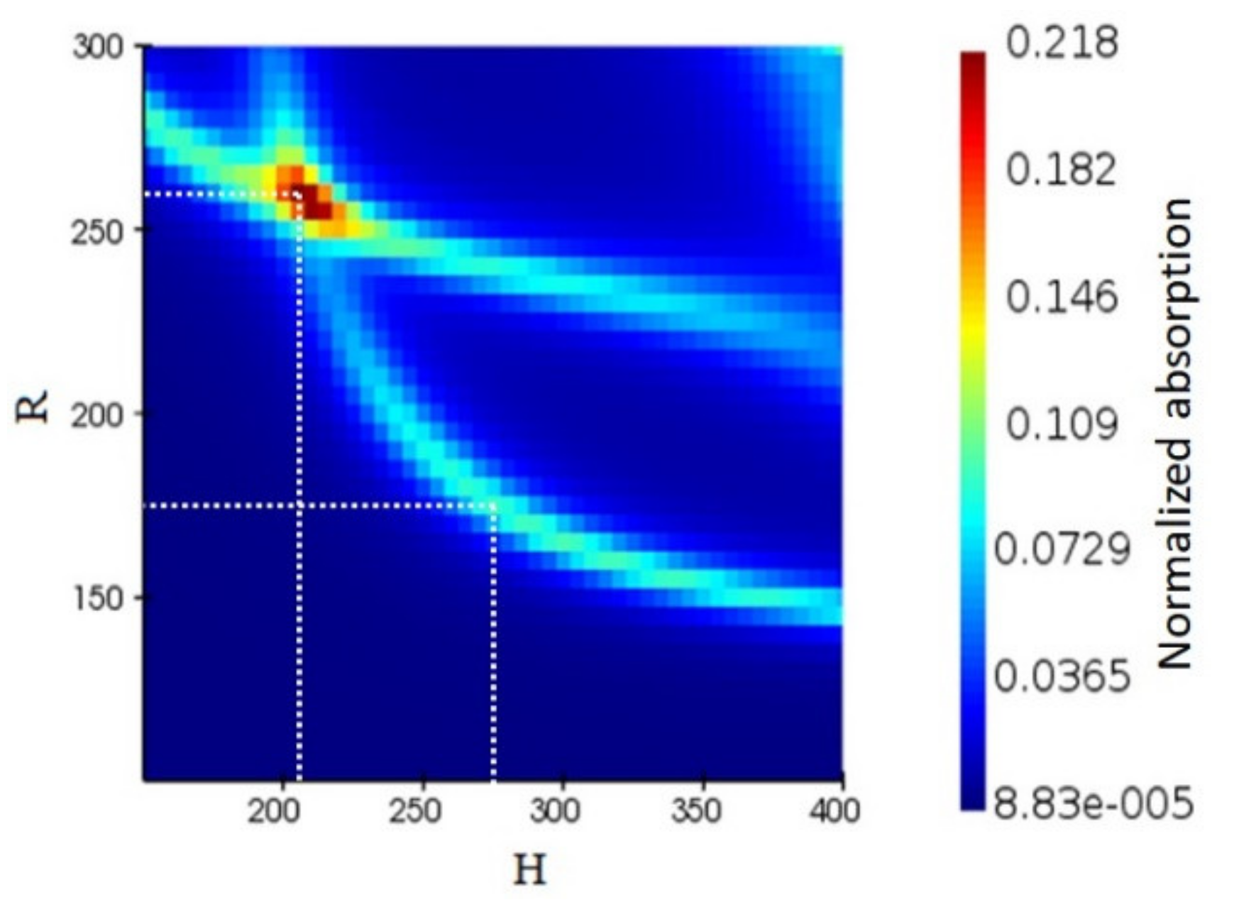
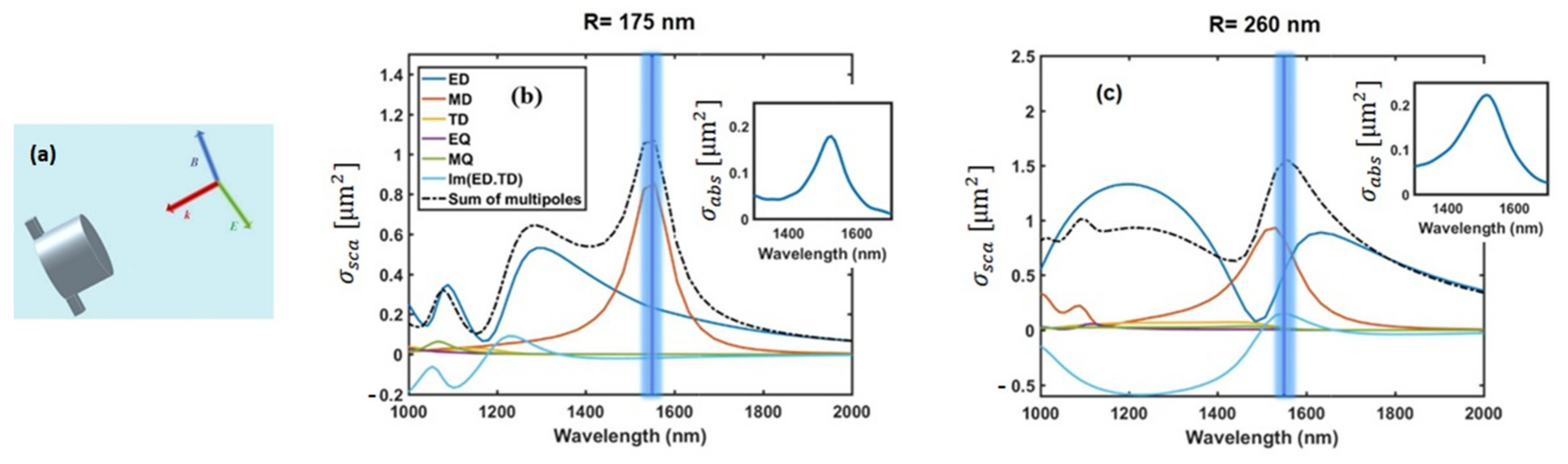
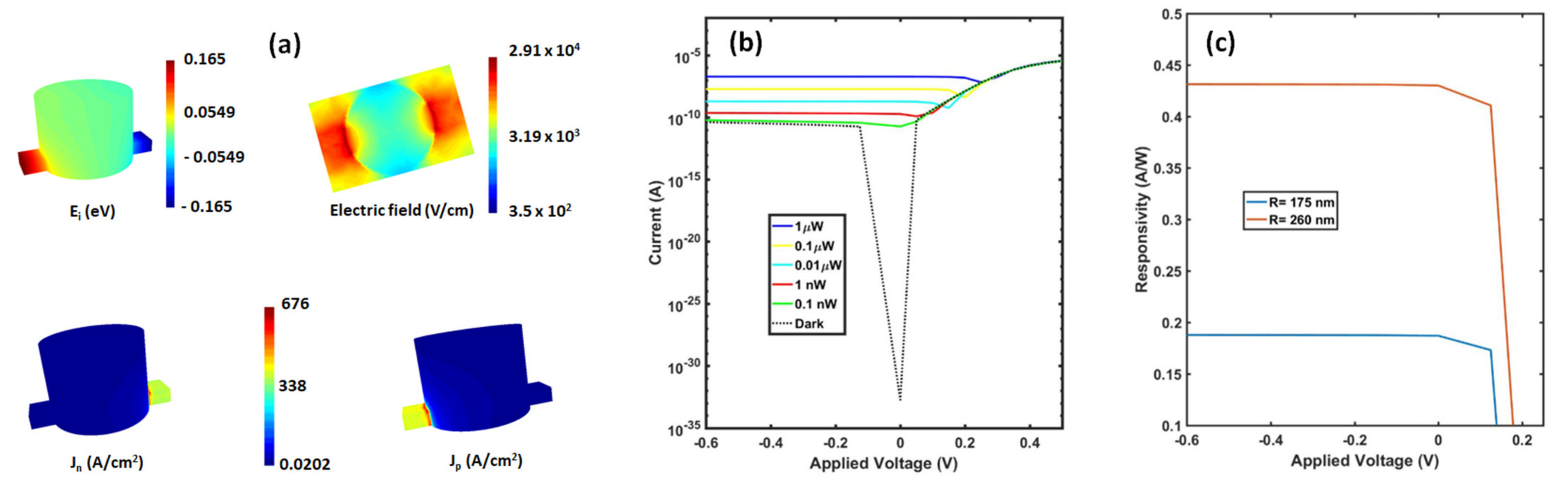
3.1. Optical Design
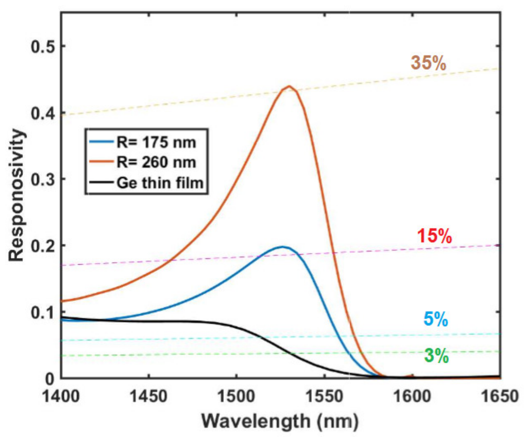
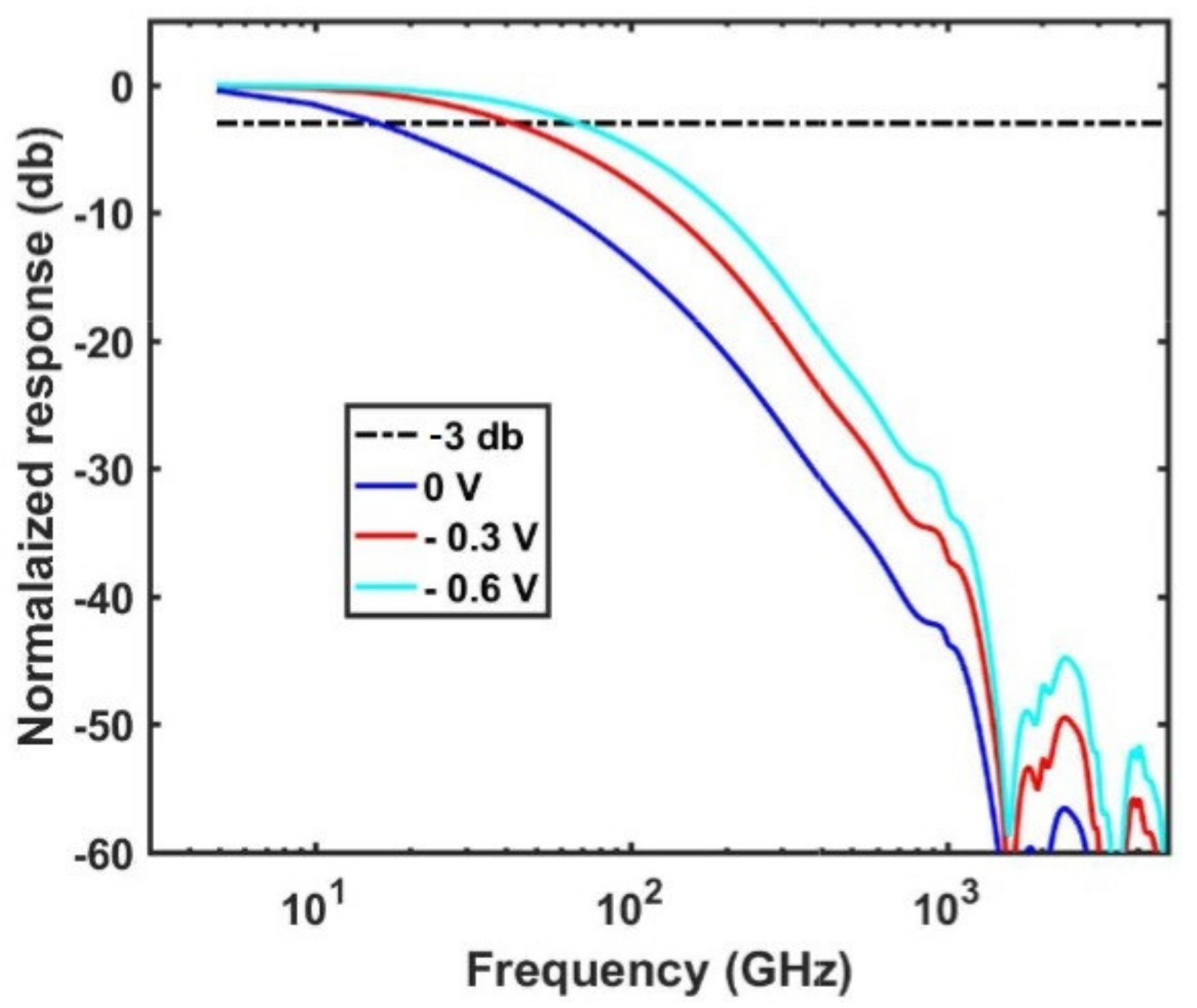
3.2. Electrical Response
4. Conclusions
Author Contributions
Funding
Data Availability Statement
Conflicts of Interest
References
- Augel, L.; Kawaguchi, Y.; Bechler, S.; Körner, R.; Schulze, J.; Uchida, H.; Fischer, I.A. Integrated Collinear Refractive Index Sensor with Ge PIN Photodiodes. ACS Photonics 2018, 5, 4586–4593. [Google Scholar] [CrossRef]
- Rogalski, A.; Antoszewski, J.; Faraone, L. Third-generation infrared photodetector arrays. J. Appl. Phys. 2009, 105, 091101. [Google Scholar] [CrossRef]
- Colace, L.; Assanto, G. Germanium on Silicon for Near-Infrared Light Sensing. IEEE Photonics J. 2009, 1, 69–79. [Google Scholar] [CrossRef]
- Rasmussen, T.S.; Yu, Y.; Mork, J. All-optical non-linear activation function for neuromorphic photonic computing using semiconductor Fano lasers. Opt. Lett. 2020, 45, 3844–3847. [Google Scholar] [CrossRef]
- Kittel, C. Introduction to Solid State Physics, 6th ed.; John Wiley & Sons: New York, NY, USA, 1986. [Google Scholar]
- Kivshar, Y.; Miroshnichenko, A.E. Meta-Optics with Mie Resonances. Opt. Photonics News 2017, 28, 24–31. [Google Scholar] [CrossRef]
- Xu, L.; Masoudian Saadabad, R.; Cai, M.; Miroshnichenko, A.E. Toroidal dipolar excitations in all-dielectric nanostructures. J. Physics Conf. Ser. 2020, 1461, 12191. [Google Scholar] [CrossRef]
- Mitrofanov, O.; Hale, L.L.; Vabishchevich, P.P.; Luk, T.S.; Addamane, S.J.; Reno, J.L.; Brener, I. Perfectly absorbing dielectric metasurfaces for photodetection. APL Photonics 2020, 5, 101304. [Google Scholar] [CrossRef]
- Zhao, Z.; Liu, J.; Liu, Y.; Zhu, N. High-speed photodetectors in optical communication system. J. Semicond. 2017, 38, 121001. [Google Scholar] [CrossRef]
- Miroshnichenko, A.E.; Evlyukhin, A.B.; Yu, Y.F.; Bakker, R.M.; Chipouline, A.; Kuznetsov, A.I.; Luk’Yanchuk, B.; Chichkov, B.N.; Kivshar, Y.S. Nonradiating anapole modes in dielectric nanoparticles. Nat. Commun. 2015, 6, 8069. [Google Scholar] [CrossRef] [PubMed]
- Krasnok, A.E.; Belov, P.A.; Miroshnichenko, A.E.; Kuznetsov, A.I.; Luk’Yanchuk, B.S.; Kivshar, Y.S. All-Dielectric Optical Nanoantennas. Prog. Compact. Antennas 2014, 601–602. [Google Scholar] [CrossRef]
- Zhu, X.; Lin, F.; Zhang, Z.; Chen, X.; Huang, H.; Wang, D.; Tang, J.; Fang, X.; Fang, D.; Ho, J.C.; et al. Enhancing Performance of a GaAs/AlGaAs/GaAs Nanowire Photodetector Based on the Two-Dimensional Electron–Hole Tube Structure. Nano Lett. 2020, 20, 2654–2659. [Google Scholar] [CrossRef]
- Zhu, X.; Lin, F.; Chen, X.; Zhang, Z.; Chen, X.; Wang, D.; Tang, J.; Fang, X.; Fang, D.; Liao, L.; et al. Influence of the depletion region in GaAs/AlGaAs quantum well nanowire photodetector. Nanotechnology 2020, 31, 444001. [Google Scholar] [CrossRef] [PubMed]
- Chen, X.; Wang, D.; Wang, T.; Yang, Z.; Zou, X.; Wang, P.; Luo, W.; Li, Q.; Liao, L.; Hu, W.; et al. Enhanced Photoresponsivity of a GaAs Nanowire Metal-Semiconductor-Metal Photodetector by Adjusting the Fermi Level. ACS Appl. Mater. Interfaces 2019, 11, 33188–33193. [Google Scholar] [CrossRef] [PubMed]
- Li, S.Q.; Solanki, A.; Frigerio, J.; Chrastina, D.; Isella, G.; Zheng, C.; Ahnood, A.; Ganesan, K.; Crozier, K.B. Vertical Ge–Si Nanowires with Suspended Graphene Top Contacts as Dynamically Tunable Multispectral Photodetectors. ACS Photonics 2019, 6, 735–742. [Google Scholar] [CrossRef]
- Solanki, A.; Li, S.; Park, H.; Crozier, K.B. Harnessing the Interplay between Photonic Resonances and Carrier Extraction for Narrowband Germanium Nanowire Photodetectors Spanning the Visible to Infrared. ACS Photonics 2017, 5, 520–527. [Google Scholar] [CrossRef]
- Calzadilla, V.V.D.; Romeira, B.B.P.; Pagliano, F.F.; Birindelli, S.S.; Rodriguez, A.A.H.; Van Veldhoven, P.R.; Smit, M.M.; Fiore, A.A.; Heiss, D.D. Waveguide-coupled nanopillar metal-cavity light-emitting diodes on silicon. Nat. Commun. 2017, 8, 14323. [Google Scholar] [CrossRef]
- Palik, E.D. Handbook of Optical Constants of Solids; Academic Press: New York, NY, USA, 1985. [Google Scholar]
- Vivien, L.; Polzer, A.; Marris-Morini, D.; Osmond, J.; Hartmann, J.M.; Crozat, P.; Cassan, E.; Kopp, C.; Zimmermann, H.; Fédéli, J.M. Zero-bias 40Gbit/s germanium waveguide photodetector on silicon. Opt. Express 2012, 20, 1096–1101. [Google Scholar] [CrossRef] [PubMed]
- Chen, H.; Verheyen, P.; De Heyn, P.P.; Lepage, G.; De Coster, J.; Balakrishnan, S.; Absil, P.; Yao, W.W.; Shen, L.L.; Roelkens, G.G.; et al. −1 V bias 67 GHz bandwidth Si-contacted germanium waveguide p-i-n photodetector for optical links at 56 Gbps and beyond. Opt. Express 2016, 24, 4622–4631. [Google Scholar] [CrossRef]
- Virot, L.; Benedikovic, D.; Szelag, B.; Alonso-Ramos, C.; Karakus, B.; Hartmann, J.-M.; Le Roux, X.; Crozat, P.; Cassan, E.; Marris-Morini, D.; et al. Integrated waveguide PIN photodiodes exploiting lateral Si/Ge/Si heterojunction. Opt. Express 2017, 25, 19487–19496. [Google Scholar] [CrossRef]
- Lin, Y.; Lee, K.H.; Bao, S.; Guo, X.; Wang, H.; Michel, J.; Tan, C.S. High-efficiency normal-incidence vertical p-i-n photodetectors on a germanium-on-insulator platform. Photonics Res. 2017, 5, 702–709. [Google Scholar] [CrossRef]
- Salamin, Y.; Ma, P.; Baeuerle, B.; Emboras, A.; Fedoryshyn, Y.M.; Heni, W.; Cheng, B.; Josten, A.; Leuthold, J. 100 GHz Plasmonic Photodetector. ACS Photonics 2018, 5, 3291–3297. [Google Scholar] [CrossRef]
- Boriskina, S.V.; Cooper, T.A.; Zeng, L.; Ni, G.; Tong, J.K.; Tsurimaki, Y.; Huang, Y.; Meroueh, L.; Mahan, G.; Chen, G. Losses in plasmonics: From mitigating energy dissipation to embracing loss-enabled functionalities. Adv. Opt. Photonics 2017, 9, 775–827. [Google Scholar] [CrossRef]
- Vyshnevyy, A.A.; Fedyanin, D.Y. Self-Heating and Cooling of Active Plasmonic Waveguides. ACS Photonics 2015, 3, 51–57. [Google Scholar] [CrossRef]
- Shirdel-Havar, A.H.; Masoudian Saadabad, R. Ballistic-diffusive approximation for the thermal dynamics of metallic nanoparticles in nanocomposite materials. J. Appl. Phys. 2015, 117, 114304. [Google Scholar] [CrossRef]
- Cole, M.A.; Powell, D.A.; Shadrivov, I.V. Strong terahertz absorption in all-dielectric Huygens’ metasurfaces. Nanotechnology 2016, 27, 424003. [Google Scholar] [CrossRef] [PubMed]
- Siday, T.; Vabishchevich, P.P.; Hale, L.L.; Harris, C.T.; Luk, T.S.; Reno, J.L.; Brener, I.; Mitrofanov, O. Terahertz Detection with Perfectly-Absorbing Photoconductive Metasurface. Nano Lett. 2019, 19, 2888–2896. [Google Scholar] [CrossRef]
- Gongora, J.S.T.; Miroshnichenko, A.E.; Kivshar, Y.S.; Fratalocchi, A. Anapole nanolasers for mode-locking and ultrafast pulse generation. Nat. Commun. 2017, 8, 15535. [Google Scholar] [CrossRef]
- Zhou, Z.; He, J.; Wang, R.; Li, C.; Yu, J. Normal incidence p–i–n Ge heterojunction photodiodes on Si substrate grown by ultrahigh vacuum chemical vapor deposition. Opt. Commun. 2010, 283, 3404–3407. [Google Scholar] [CrossRef]
- Raab, R.E.; de Lange, O.L. Multipole Theory in Electromagnetism; Oxford University Press: New York, NY, USA, 2005. [Google Scholar]
- Gurvitz, E.A.; Ladutenko, K.S.; Dergachev, P.A.; Evlyukhin, A.B.; Miroshnichenko, A.E.; Shalin, A.S. The High-Order Toroidal Moments and Anapole States in All-Dielectric Photonics. Laser Photonics Rev. 2019, 13, 1–13. [Google Scholar] [CrossRef]
- Evlyukhin, A.B.; Fischer, T.; Reinhardt, C.; Chichkov, B.N. Optical theorem and multipole scattering of light by arbitrarily shaped nanoparticles. Phys. Rev. B 2016, 94, 205434. [Google Scholar] [CrossRef]
- Terekhov, P.D.; Baryshnikova, K.V.; Artemyev, Y.A.; Karabchevsky, A.; Shalin, A.S.; Evlyukhin, A.B. Multipolar response of nonspherical silicon nanoparticles in the visible and near-infrared spectral ranges. Phys. Rev. B 2017, 96, 35443. [Google Scholar] [CrossRef]
- Li, J.; Xin, X.-X.; Shao, J.; Wang, Y.-H.; Li, J.-Q.; Zhou, L.; Dong, Z.-G. From non- to super-radiating manipulation of a dipolar emitter coupled to a toroidal metastructure. Opt. Express 2015, 23, 29384–29389. [Google Scholar] [CrossRef] [PubMed]
- Terekhov, P.D.; Baryshnikova, K.; Greenberg, Y.; Fu, Y.H.; Evlyukhin, A.B.; Shalin, A.S.; Karabchevsky, A. Enhanced absorption in all-dielectric metasurfaces due to magnetic dipole excitation. Sci. Rep. 2019, 9, 1–9. [Google Scholar] [CrossRef]
- Feng, T.; Xu, Y.; Zhang, W.; Miroshnichenko, A.E. Ideal Magnetic Dipole Scattering. Phys. Rev. Lett. 2017, 118, 173901. [Google Scholar] [CrossRef] [PubMed]
- Agrawal, G.P. Fiber-Optic Communications Systems, 3rd ed.; John Wiley & Sons: New York, NY, USA, 2002. [Google Scholar]
- Shen, Y.; Gaskins, J.; Xie, X.; Foley, B.M.; Cheaito, R.; Hopkins, P.E.; Campbell, J.C. Thermal Analysis of High-Power Flip-Chip-Bonded Photodiodes. J. Light. Technol. 2017, 35, 4242–4246. [Google Scholar] [CrossRef]
- Xue, H.-Y.; Xue, C.; Cheng, B.; Yu, Y.-D.; Wang, Q.-M. High-Saturation-Power and High-Speed Ge-on-SOI p-i-n Photodetectors. IEEE Electron. Device Lett. 2010, 31, 701–703. [Google Scholar] [CrossRef]
- Marozas, B.T.; Hughes, W.D.; Du, X.; Sidor, D.E.; Savich, G.R.; Wicks, G. Surface dark current mechanisms in III-V infrared photodetectors [Invited]. Opt. Mater. Express 2018, 8, 1419–1424. [Google Scholar] [CrossRef]
- Singh, J. Semiconductor Optoelectronics: Physics and Technology; McGraw-Hill: Singapor, 1995. [Google Scholar]
- Wang, J.; Lee, S. Ge-Photodetectors for Si-Based Optoelectronic Integration. Sensors 2011, 11, 696–718. [Google Scholar] [CrossRef]
- Park, H.; Dan, Y.; Seo, K.; Yu, Y.J.; Duane, P.K.; Wober, M.; Crozier, K.B. Filter-Free Image Sensor Pixels Comprising Silicon Nanowires with Selective Color Absorption. Nano Lett. 2014, 14, 1804–1809. [Google Scholar] [CrossRef]
- Armin, A.; Vuuren, R.D.J.-V.; Kopidakis, N.; Burn, P.L.; Meredith, P. Narrowband light detection via internal quantum efficiency manipulation of organic photodiodes. Nat. Commun. 2015, 6, 6343. [Google Scholar] [CrossRef]


Publisher’s Note: MDPI stays neutral with regard to jurisdictional claims in published maps and institutional affiliations. |
© 2021 by the authors. Licensee MDPI, Basel, Switzerland. This article is an open access article distributed under the terms and conditions of the Creative Commons Attribution (CC BY) license (http://creativecommons.org/licenses/by/4.0/).
Share and Cite
Masoudian Saadabad, R.; Pauly, C.; Herschbach, N.; Neshev, D.N.; Hattori, H.T.; Miroshnichenko, A.E. Highly Efficient Near-Infrared Detector Based on Optically Resonant Dielectric Nanodisks. Nanomaterials 2021, 11, 428. https://doi.org/10.3390/nano11020428
Masoudian Saadabad R, Pauly C, Herschbach N, Neshev DN, Hattori HT, Miroshnichenko AE. Highly Efficient Near-Infrared Detector Based on Optically Resonant Dielectric Nanodisks. Nanomaterials. 2021; 11(2):428. https://doi.org/10.3390/nano11020428
Chicago/Turabian StyleMasoudian Saadabad, Reza, Christian Pauly, Norbert Herschbach, Dragomir N. Neshev, Haroldo T. Hattori, and Andrey E. Miroshnichenko. 2021. "Highly Efficient Near-Infrared Detector Based on Optically Resonant Dielectric Nanodisks" Nanomaterials 11, no. 2: 428. https://doi.org/10.3390/nano11020428
APA StyleMasoudian Saadabad, R., Pauly, C., Herschbach, N., Neshev, D. N., Hattori, H. T., & Miroshnichenko, A. E. (2021). Highly Efficient Near-Infrared Detector Based on Optically Resonant Dielectric Nanodisks. Nanomaterials, 11(2), 428. https://doi.org/10.3390/nano11020428