Article

Broadband Optical Properties of Atomically Thin PtS2 and PtSe2

by
Georgy A. Ermolaev
1,
Kirill V. Voronin
1,
Mikhail K. Tatmyshevskiy
1,
Arslan B. Mazitov
1,2,
Aleksandr S. Slavich
1,
Dmitry I. Yakubovsky
1,
Andrey P. Tselin
1,
Mikhail S. Mironov
1,
Roman I. Romanov
3,
Andrey M. Markeev
1,
Ivan A. Kruglov
1,2,
Sergey M. Novikov
1,
Andrey A. Vyshnevyy
1,
Aleksey V. Arsenin
1,4 and
Valentyn S. Volkov
1,4,*
1
Center for Photonics and 2D Materials, Moscow Institute of Physics and Technology, 9 Institutsky Lane, 141700 Dolgoprudny, Russia
2
Dukhov Research Institute of Automatics (VNIIA), 22 Suschevskaya St., 127055 Moscow, Russia
3
Moscow Engineering Physics Institute, National Research Nuclear University MEPhI, 31 Kashirskoe Sh., 115409 Moscow, Russia
4
GrapheneTek, Skolkovo Innovation Center, 143026 Moscow, Russia
*
Author to whom correspondence should be addressed.
Nanomaterials 2021, 11(12), 3269; https://doi.org/10.3390/nano11123269
Submission received: 4 November 2021 / Revised: 21 November 2021 / Accepted: 29 November 2021 / Published: 1 December 2021
(This article belongs to the Section 2D and Carbon Nanomaterials)

Abstract

:
Noble transition metal dichalcogenides (TMDCs) such as PtS2 and PtSe2 show significant potential in a wide range of optoelectronic and photonic applications. Noble TMDCs, unlike standard TMDCs such as MoS2 and WS2, operate in the ultrawide spectral range from ultraviolet to mid-infrared wavelengths; however, their properties remain largely unexplored. Here, we measured the broadband (245–3300 nm) optical constants of ultrathin PtS2 and PtSe2 films to eliminate this gap and provide a foundation for optoelectronic device simulation. We discovered their broadband absorption and high refractive index both theoretically and experimentally. Based on first-principle calculations, we also predicted their giant out-of-plane optical anisotropy for monocrystals. As a practical illustration of the obtained optical properties, we demonstrated surface plasmon resonance biosensors with PtS2 or PtSe2 functional layers, which dramatically improves sensor sensitivity by 60 and 30%, respectively.

1. Introduction

During the last decade, atomically thin transition metal dichalcogenides (TMDCs) have revolutionized optoelectronics [1,2,3,4,5] thanks to their unique optical and electronic properties, including thickness-dependent bandgap [6], high carrier mobility [7], giant anisotropy [8], high refractive index [9,10], strain-dependent properties [11] and strongly bound excitons [12]. The most well-known materials with these phenomena are the group-VI TMDCs with general structure MX2, where M = Mo or W and X = S, Se, or Te [13]. However, despite their enormous potential and tremendous results, they have two significant constraints. First, their bandgap ranges from 1 to 2 eV [14], making group-VI TMDCs rather limited to visible range applications. Second, group-VI TMDCs have low environmental stability [15], which significantly reduces their application possibilities. These problems motivated an intensive search for stable layered materials with a bandgap in the infrared range.
As a result, approximately 5000 potentially useful two-dimensional materials have recently been found [16]. Among them, group-X noble TMDCs (with general structure MX2, where M = Pt or Pd and X = S, Se, or Te) stands out, owing to their widely tunable bandgap from visible (for monolayers) to mid-infrared (for few-layers) spectral intervals [17], high electron mobility [18] and remarkable air and liquid stability [19,20]. Broadband photodetectors [21], lasing [22], field-effect transistors [23], label-free sensors [20,24], holography [25], and ultrathin lenses [26], for example, have previously proved the advantages of atomically thin films (about 5 nm) of group-X TMDCs for optoelectronics. With such a wide spectrum of optoelectronic applications, precise knowledge of group-X TMDCs optical properties is of paramount importance. The reported experimental works focused on Raman fingerprints [27,28], absorbance [18,29], and photoconductivity [30,31] of group-X TMDCs. However, there are limited reports [25,32,33,34] on their optical constants (refractive index n and extinction coefficient k), which are crucial for predicting the performance of optoelectronic devices. Furthermore, these works [25,32,33,34] provide data only for a narrow spectral range required for their specific task. Therefore, a determination of the broadband dielectric function for group-X TMDCs is in high demand.
This work focuses on the optical properties of atomically thin PtS2 and PtSe2, which are typical representatives of group-X TMDCs. Through spectroscopic ellipsometry measurements, we accurately retrieved their broadband optical constants from ultraviolet to mid-infrared wavelengths (from 245 to 3300 nm). For all of the measured wavelengths, we discovered that PtS2 and PtSe2 exhibit non-zero extinction coefficients (k > 0), which explains recent advances of PtS2 and PtSe2 in photodetection [21] for these spectral intervals. Additionally, our findings reveal a high refractive index (n ~ 4) of these materials, which makes them perfect candidates for all-dielectric nano-photonics [35,36,37].

2. Materials and Methods

2.1. Materials

Full area coverage PtS2 and PtSe2 multilayers were purchased from 2d Semiconductors, Inc. (2d Semiconductors Inc., Scottsdale, AZ, USA). The samples were grown on c-cut sapphire substrates by chemical vapor deposition (CVD) using the highest purity (6N) gases (N2/H2) and precursors (S powder and Pt films) in semiconductor-grade facilities with subsequent water-assisted transfer on a 300 nm SiO2/Si substrate.

2.2. Raman Characterization

The experimental setup used for Raman measurements was a Horiba LabRAM HR Evolution confocal scanning Raman microscope (Horiba Ltd., Kyoto, Japan). All measurements were carried out using linearly polarized excitation at wavelength 632.8 nm; 1800 lines/mm diffraction grating, and × 100 objective (N.A. = 0.90), whereas we used unpolarized detection to have a significant signal-to-noise ratio. The spot size was approximately 0.43 µm. The Raman spectra were recorded with 0.75 mW and an integration time of 10 s at each point. The statistics were collected with 15 points for each sample, and the observed variation of the intensity for the spectra was less than 5%.

2.3. XPS Characterization

The chemical state of the elements in the film was analyzed by X-ray photoelectron spectroscopy (XPS) in the Theta Probe tool (Thermo Scientific K-Alpha, Waltham, MA, USA) under ultrahigh vacuum conditions (base pressure < 10−9 mBar) with a monochromatic Al-Kα X-ray source (1486.6 eV). Photoelectron spectra were acquired using fixed analyzer transmission (FAT) mode with 50 eV pass energy. The spectrometer energy scale was calibrated using C1s line position at 284.5 eV.

2.4. Atomic Force Microscopy

The thickness and surface morphology of PtS2 and PtSe2 films were accurately characterized by an atomic force microscope (NT-MDT N’tegra tool, Moscow, Russia) using AFM in peak-force mode under ambient conditions. AFM measurements were carried out using ETALON, HA_NC silicon tips from TipsNano (TipsNano, Tallin, Estonia) with a spring constant of 3.5 N/m, a head curvature radius < 10 nm and a resonant frequency of 140 kHz. Images of PtS2 and PtSe2 surfaces were taken over a 3 × 3 µm2 area with a scan rate of 0.2 Hz; after that, data were analyzed by Gwyddion software.

2.5. Optical Visualization

The surface images (2400 × 2400 pixels) of PtS2 and PtSe2 were captured by an optical microscope (Nikon LV150L, Tokyo, Japan) with a digital camera DS-Fi3.

2.6. Scanning Electron Microscopy

A scanning electron microscope JEOL JSM-7001F (JEOL Ltd., Tokyo, Japan) accompanied by a Schottky emitter in secondary electron imaging mode with a voltage of 30 keV and current of 67 µA, and a working distance of approximately 6.3 mm, was used to study surface features and homogeneity of PtS2 and PtSe2 films surfaces in detail within different areas using a 1960 × 1280 pixel scan.

2.7. X-ray Diffraction

An X-ray powder diffractometer (XRD, Thermo ARL X’TERA, Waltham, MA, USA) equipped with Cu Kα radiation λ = 0154 nm was used to characterize the crystalline structure and phase of PtS2 and PtSe2 films. The XRD pattern was taken at ambient conditions by 2θ-scan over the range of 20–75° with a step of 0.05° and accumulation time of 2 s.

2.8. Reflectance Measurements

The spectroscopic reflection analysis was performed in the 400–975 nm spectral range on a Biolam M-1 microscope (LOMO, Saint-Petersburg, Russia) equipped with a 24 V, 100 W halogen light source and a QE65000 fiber-coupled grating spectrometer (Ocean Optics). The reflected light was collected in a backscattering configuration using an objective with magnification 100× (NA = 0.80). The experimental data represent the reflection ratio Rstr/Rref, where Rstr is the reflection measured from the structures with films and Rref is the reference from a silver mirror NT64−114 (Edmund Optics, Barrington, NJ, USA) that exhibits an average reflection of 99% between 350 and 1100 nm of light wavelength.

2.9. Ellipsometry Characterization

We used a variable-angle spectroscopic ellipsometer (VASE, J.A. Woollam Co., Lincoln, NE, USA) with a single chamber monochromator with two gratings: 1200 g/mm for visible light (245–1040 nm) with 4.6 nm bandwidth and 600 g/mm for the infrared interval (1040–3300 nm) with 9.2 nm bandwidth. Spectroscopic ellipsometry was conducted over a wide wavelength range (from 245 to 3300 nm in steps of 1 nm) and multiple angles of incidence in the range of 30° to 80° with a step size of 5°.

2.10. Mueller Matrix Measurements

To investigate the in-plane anisotropic response of PtS2 and PtSe2, we measured 11 elements of the Mueller matrix (m12, m13, m14, m21, m22, m23, m24, m31, m32, m33, m34) on an Accurion nanofilm_ep4 ellipsometer (Accurion GmbH, Goettingen, Germany) at 532 nm and 50° incident angle in rotation compensator mode.

2.11. First-Principle Calculations

The optical properties of PtS2 and PtSe2 were calculated using density functional theory (DFT) within the generalized gradient approximation [38] (Perdew–Burke–Ernzerhof functional) and the projector-augmented wave method [39] as implemented in the Vienna Ab Initio Simulation Package. The unit cell parameters of PtS2 were a = b = 0.3537 nm, c = 0.5019 nm, α = β = 90°, γ = 120°, and a = b = 0.3731 nm, c = 0.5072 nm, α = β = 90°, γ = 120° for PtSe2 [40]. A two-step approach was used: First, the atomic positions of PtS2 and PtSe2 were relaxed until the interatomic forces were less than 10−3 eV/Å, and a one-electron basis set was obtained from standard DFT calculations. Second, the real and imaginary parts of the frequency-dependent dielectric function were calculated using the GW approximation [41]. In addition, the spin–orbit interaction was included in the calculation to account for relativistic corrections to the dielectric function. The plane-wave kinetic energy cutoff was set to 700 eV, and the Γ-centered 15 × 11 × 11 k-points mesh was used to sample the first Brillouin zone.

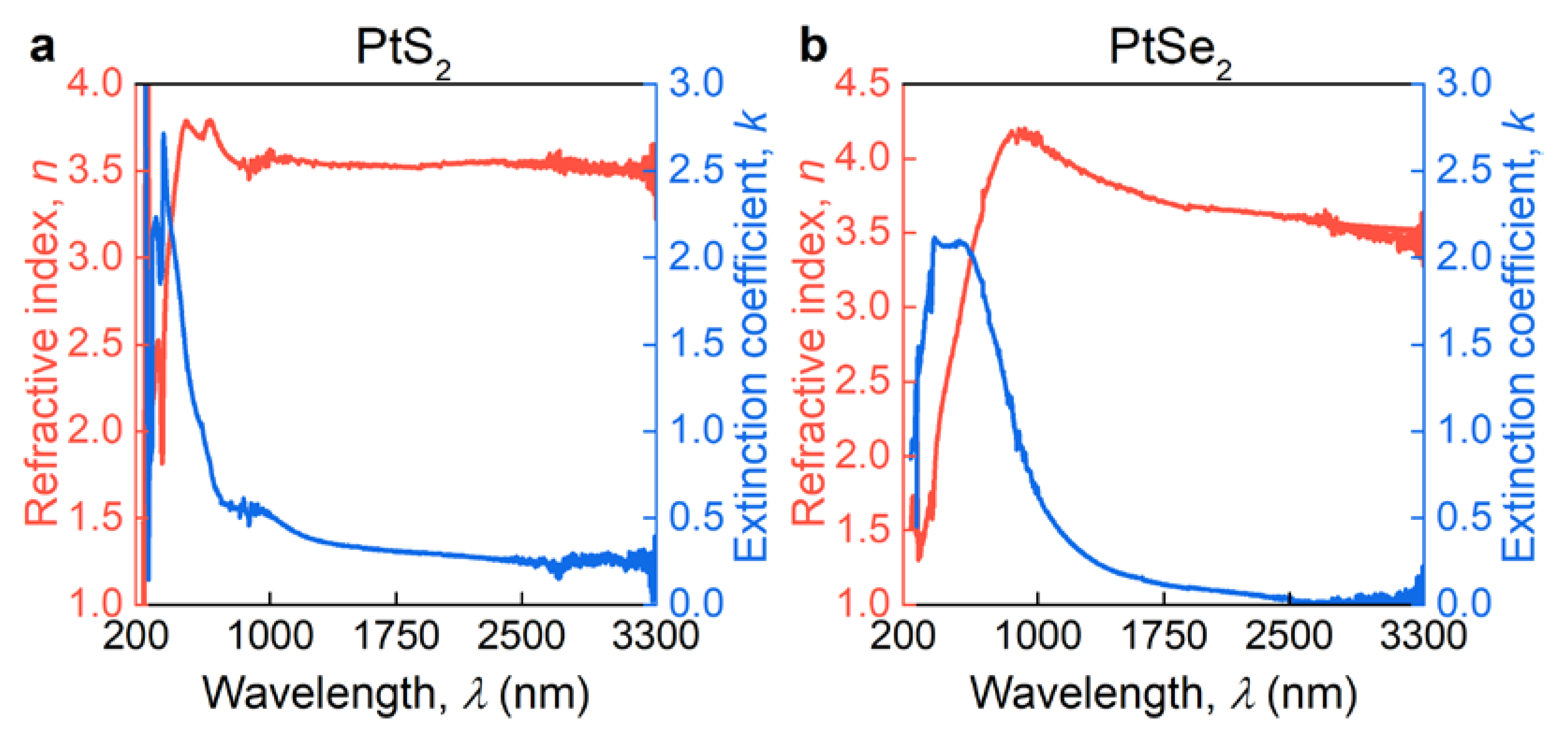
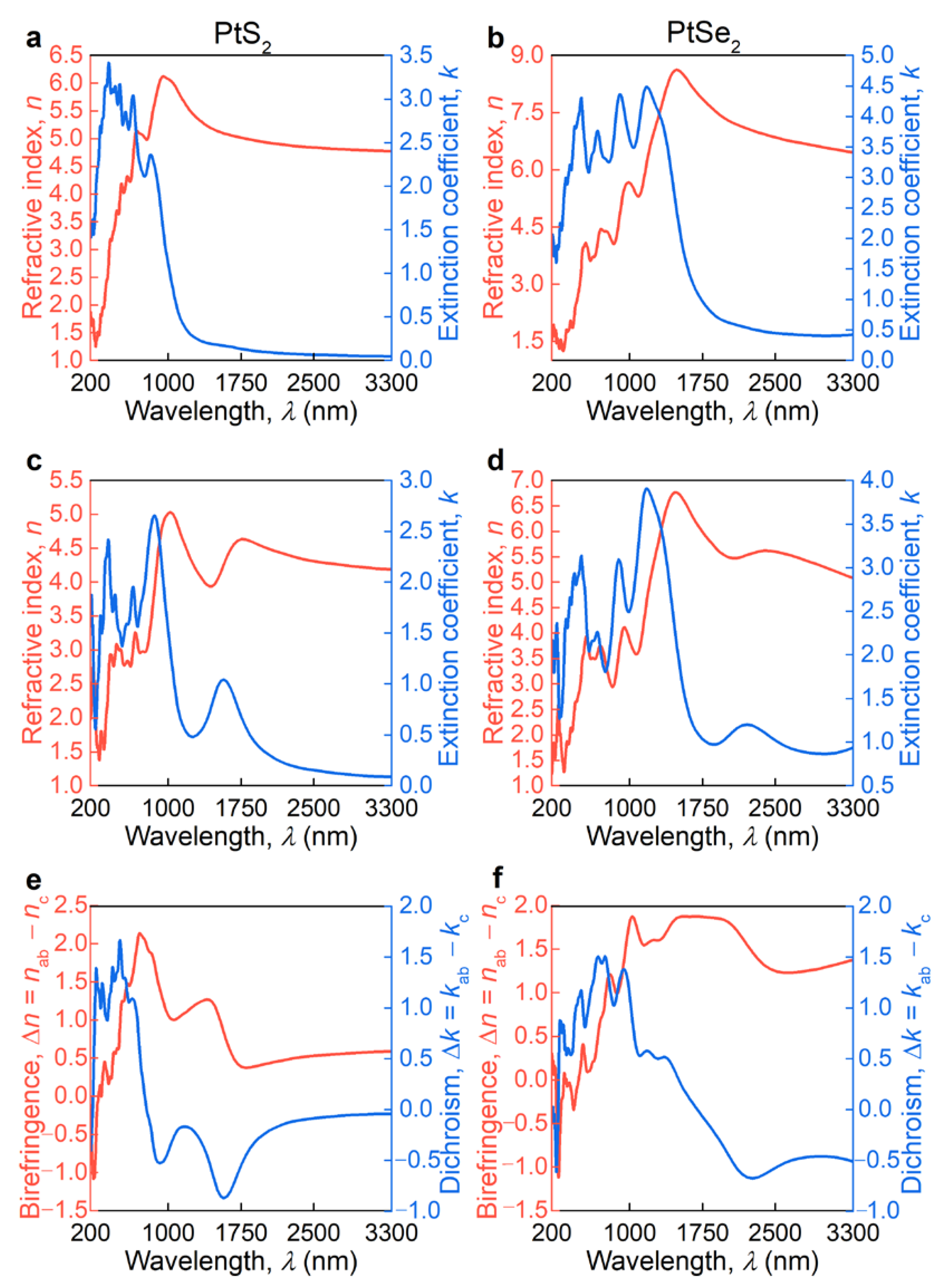
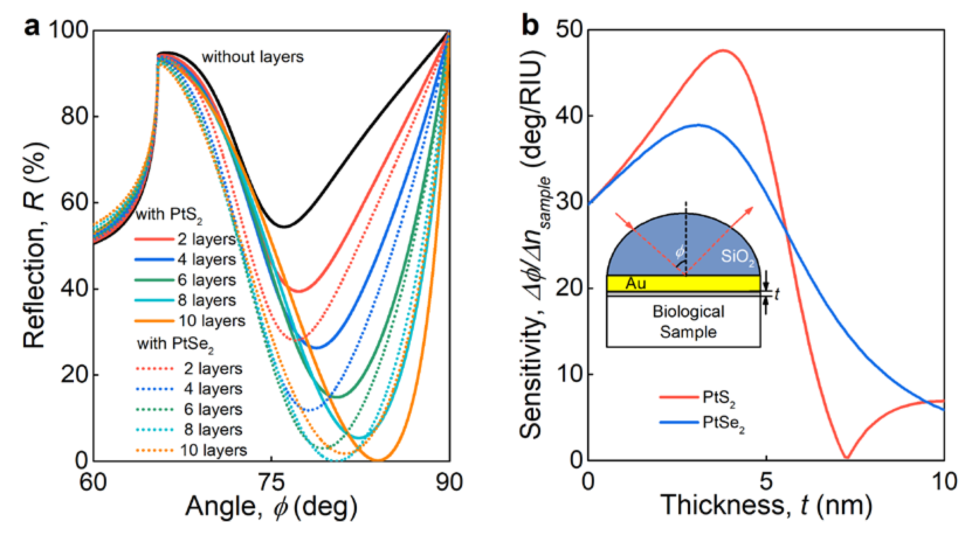
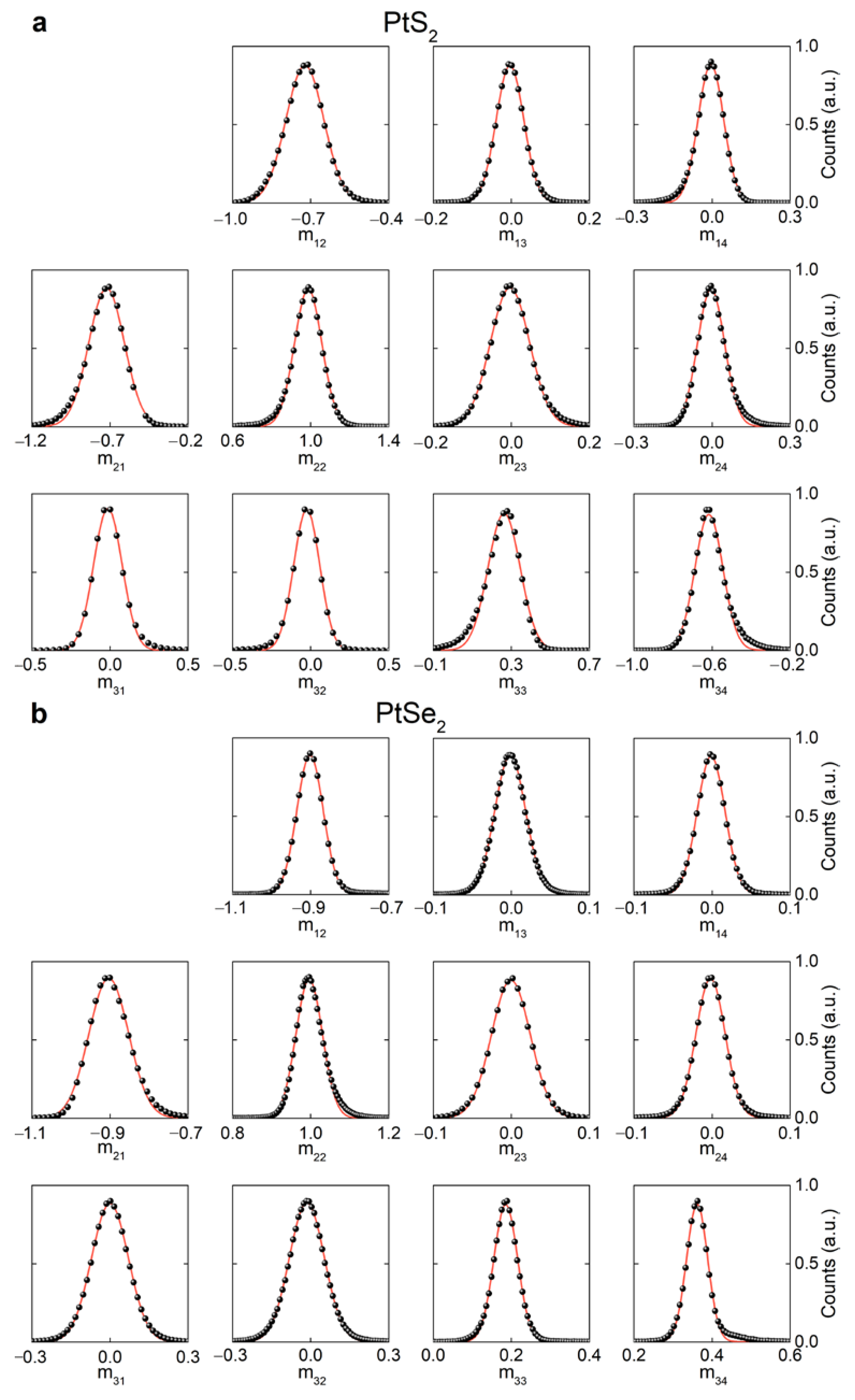
3. Results and Discussion

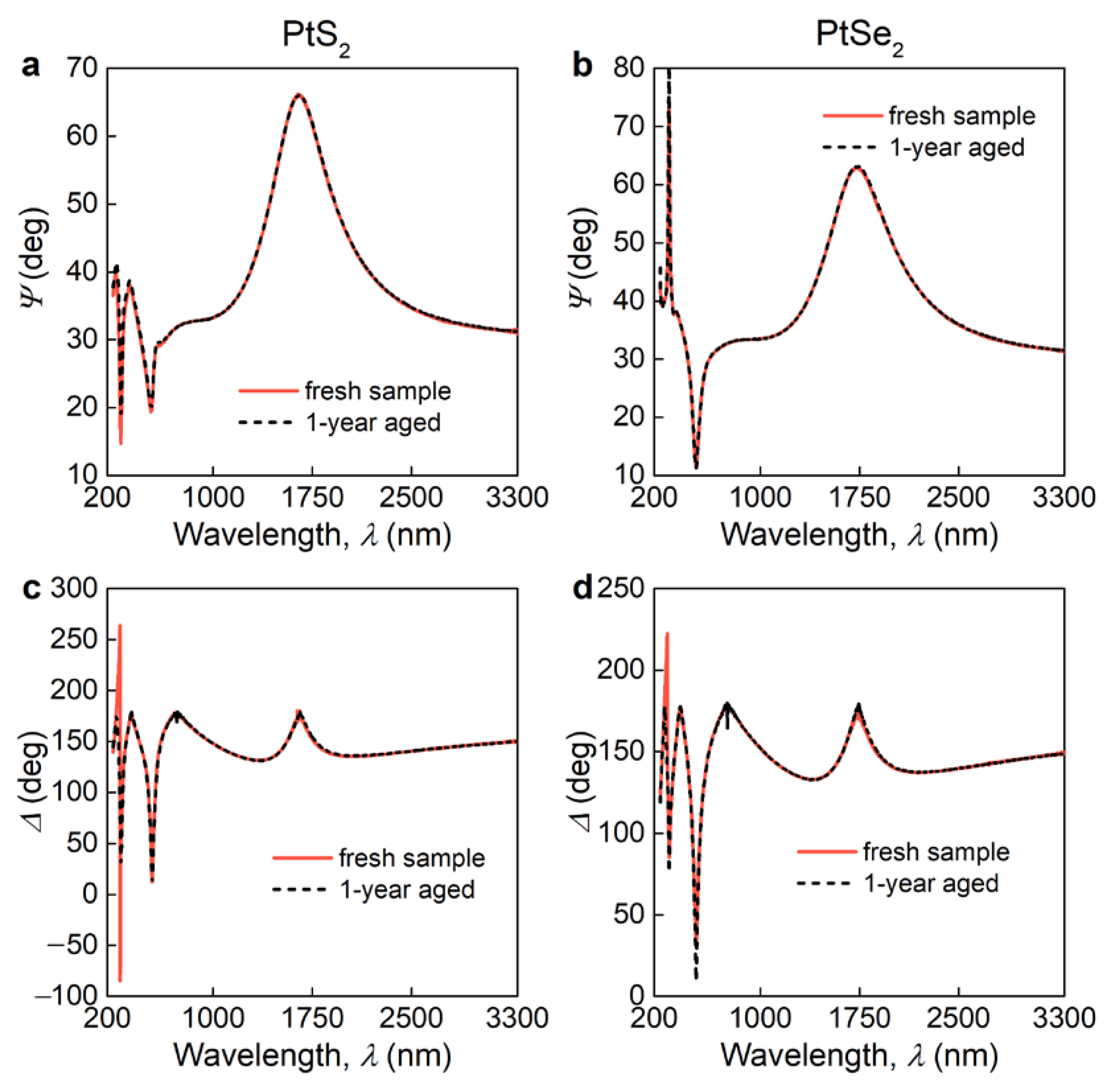
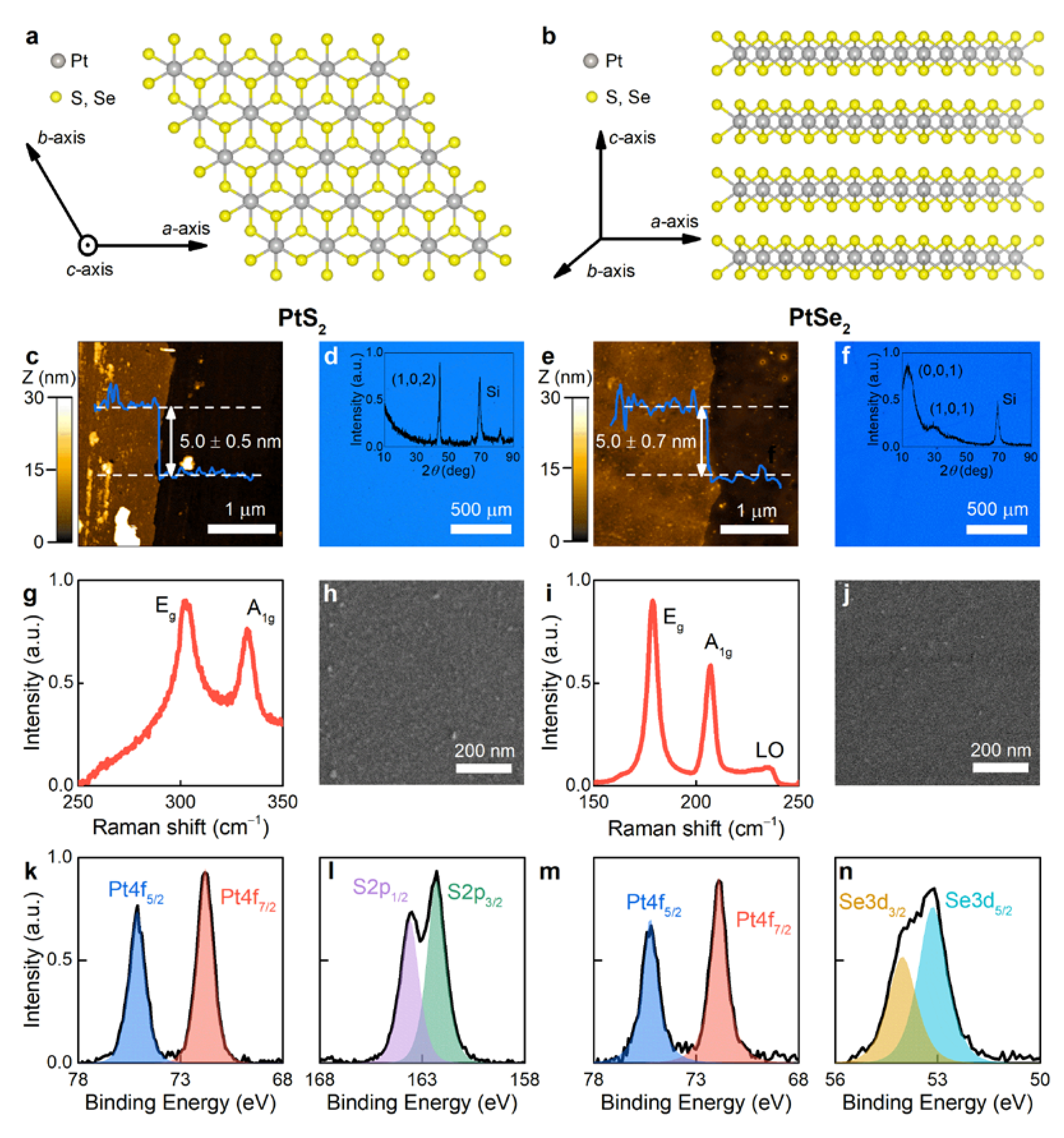
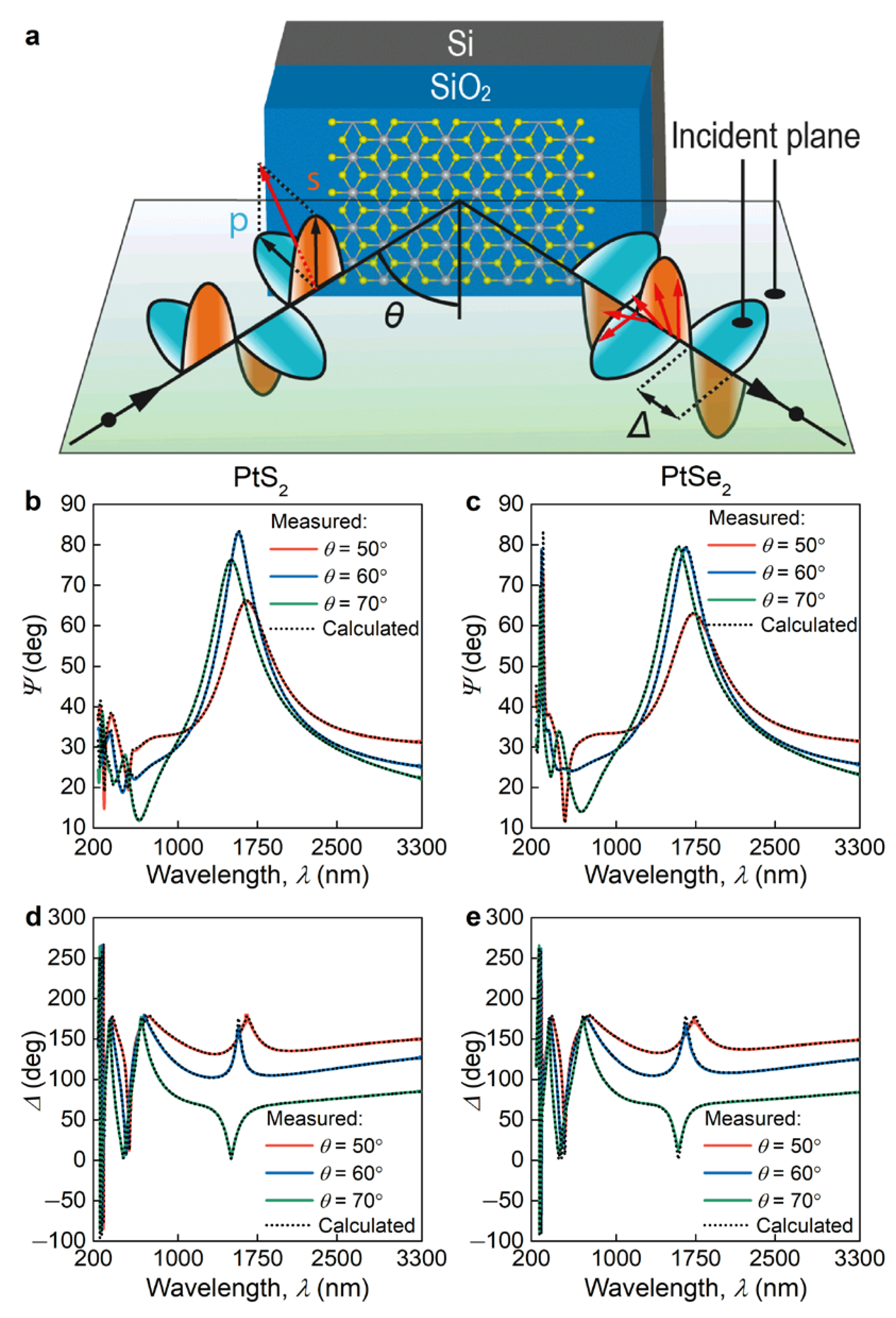
3.1. Samples Characterization

Atomically thin PtS2 and PtSe2 were prepared by chemical vapor deposition (CVD) on c-cut sapphire with subsequent water-assisted transfer on a 300 nm SiO2/Si substrate [42] to facilitate spectroscopic ellipsometry studies of optical constants, owing to interference in the thick silicon oxide. PtS2 and PtSe2 grow in the thermodynamically favored 1T-phase, as illustrated in Figure 1a,b, unlike group-VI TMDCs [43]. As shown in Figure 1c and e, the CVD-grown PtS2 and PtSe2 have a thickness of 5 nm determined by atomic force microscopy (AFM). Therefore, our films have ten layers, since the interlayer distance in PtS2 and PtSe2 is 0.5 nm [27]. Raman spectroscopy in Figure 1g,i of the obtained films reveals pronounced peaks inherent to PtS2 and PtSe2 Raman modes Eg and A1g, corresponding to in-plane and out-of-plane vibrations of chalcogen atoms (S, Se), respectively [43]. Indeed, their position (Eg ~ 300 cm−1 and A1g ~ 335 cm−1 for PtS2; Eg ~ 175 cm−1 and A1g ~ 205 cm−1 for PtS2) corresponds to few-layer PtS2 and PtSe2 [27,28] in agreement with AFM measurements. The Raman spectra do not contain photoluminescence responses in agreement with previous reports [27,28] on Raman study of PtS2 and PtSe2 at the 632.8 nm excitation wavelength. Moreover, our samples uniformly cover the substrate as confirmed by optical and scanning electron microscopy (SEM) images for PtS2 and PtSe2 in Figure 1d,h. Therefore, our samples are uniform at different scales, which is understood from the uniform color and contrast in optical and SEM images, respectively. One may notice small features of about 10 nm seen in the SEM images (Figure 1h,j), which are leftovers of the transfer process from sapphire to SiO2/Si substrate. Nevertheless, these leftovers cover less than 5% of the surface and, hence, have a negligible effect on the resulting optical constants of PtS2 and PtSe2 studied here [44]. Additionally, X-ray photoemission spectroscopy (XPS) in Figure 1k–n shows Pt 4f, S 2p, and Se 3d spectra associated with PtS2 and PtSe2 [27,28]. Finally, the crystallinity of the synthesized PtS2 and PtSe2 films was shown by measuring the X-ray diffraction (XRD) spectra displayed in the inset of Figure 1d,f.

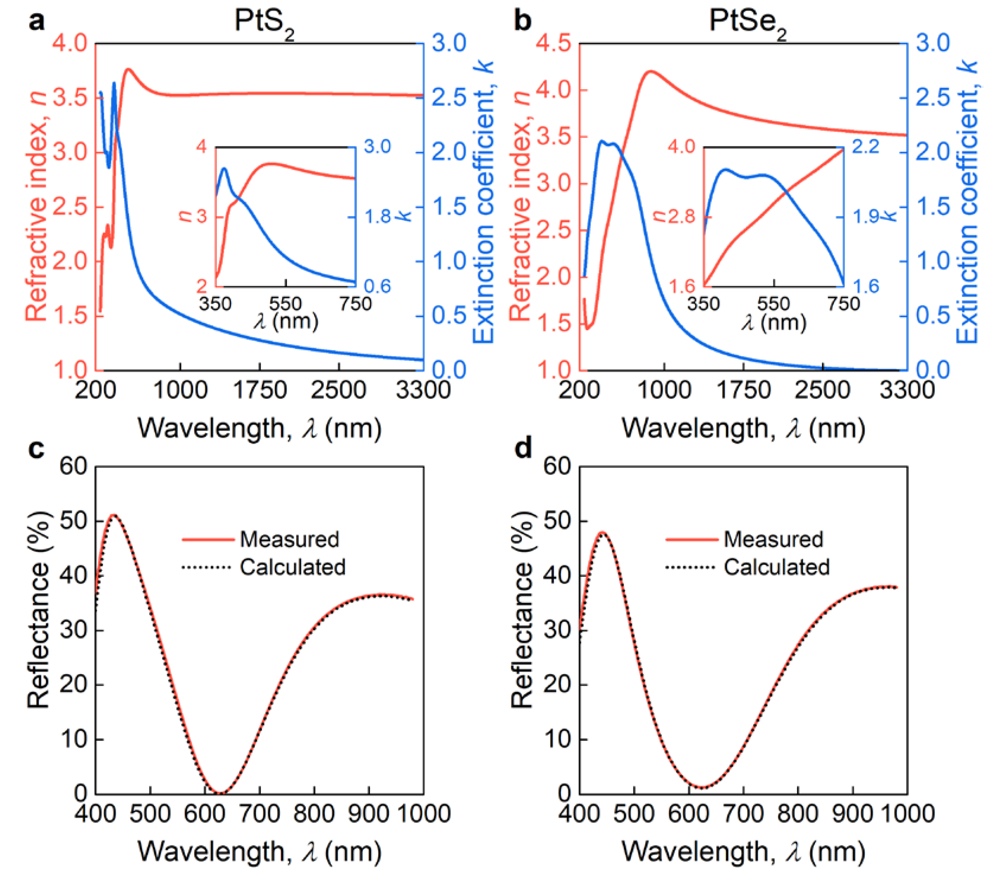
3.2. Dielectric Response Analysis

To properly quantify broadband optical properties of atomically thin PtS2 and PtSe2, we performed spectroscopic ellipsometry (SE) measurements at multiple incident angles (30–80° in 5° steps) and wavelengths (245–3300 nm in 1 nm steps). The experimental scheme of SE setup is displayed in Figure 2a. SE measures the change in polarization upon reflection in terms of Ψ and Δ (Figure 2b–e), which depends on the optical constants of the investigated sample. Hence, we need to provide an optical model to retrieve the dielectric function of PtS2 and PtSe2. First, we checked the in-plane anisotropy of our samples using the Mueller matrix method [20], in which non-zero non-diagonal elements account for in-plane optical anisotropy. In our case, zero non-diagonal elements of the Mueller matrix (Figure A1) clearly indicate the isotropic optical response of PtS2 and PtSe2 in agreement with the previous study [32]. In addition, we recorded the Ψ and Δ spectra for one-year aged samples (Figure A2), which reproduced the data in Figure 2b–e, thereby confirming the stability of PtS2 and PtSe2.
For the optical model, we used the thickness determined from AFM (Figure 1c,e), which allowed us to fix the thickness during the fitting procedure. Note that some authors fit the thickness of thin films (<10 nm) and optical constants at the same time. However, such an approach usually leads to incorrect thickness and optical constants results because of their high correlation [45]. We also used point-by-point inversion [44] to obtain the initial approximation of PtS2 and PtSe2 optical constants (Figure A3). In this approach, for each wavelength, refractive index n and extinction coefficient k are varied to achieve the best match with experimental spectra. Despite its effectiveness and ease of use, this method results in noisy data and sometimes unphysical values [45]. In contrast, the oscillator approach leads to smooth and the Kramers–Kronig consistent dielectric function [46]. As a result, in the next step, we used the Tauc–Lorentz oscillator model, which is commonly used for optical modeling of TMDCs [46,47,48]:
ε 2 = { 1 E · A E 0 C ( E E g ) 2 ( E 2 E 0 2 ) 2 + C 2 E 2 f o r   E > E g 0 f o r   E < E g
where E is the photon energy, A is the oscillator strength, C is the oscillator broadening, E g is the optical bandgap, and E 0 is the oscillator central energy, while the real part ε 1 of the dielectric function is derived from Kramers–Kronig integration plus ε to account for high energy electronic transitions. After fitting the oscillator parameters (Table 1 and Table 2), we obtained the final PtS2 and PtSe2 optical constants depicted in Figure 3a,b, which yield the perfect agreement between calculated and experimental Ψ and Δ (Figure 2b,e). The resulting oscillator parameters are collected in Table 1 and Table 2. Further, to confirm our optical constants, we recorded the reflectance spectra (Figure 3c,d) [49] and compared them with the transfer matrix calculations [50] based on the dielectric function from Figure 3a,b. Figure 3c,d show the perfect match between calculated and experimental spectra, which additionally verifies our optical constants. It is worth noting that the oscillations in the reflectance spectra (Figure 3c,d) originate from thin film interference in the SiO2 layer [51], which enhances the light–matter interaction with our samples. Of immediate interest is also the refractive index and extinction coefficient values of PtS2 and PtSe2: both materials have k > 0 in the entire spectral range and high refractive index n ~ 4. In contrast, group-VI TMDCs such as MoS2 and WS2 have zero extinction coefficient, but a similar refractive index of about 4 in the infrared range [9,46]. We also retrieved the optical constants from the first-principle calculations under the assumption of perfect crystallinity (see Methods and Figure A4a,d). Although the theoretical values deviate from experimental values due to approximation methods and the polycrystalline structure of CVD-grown films, first-principle calculations capture the major optical features of PtS2 and PtSe2: broadband absorption and strong dielectric response. Furthermore, theory predicts a giant out-of-plane optical anisotropy (Figure A4e,f), making PtS2 and PtSe2 ideal candidates for recently emerging anisotropic nano-photonics [8]. Therefore, PtS2 and PtSe2 are particularly promising for optoelectronics and nano-photonics, since their out-of-plane anisotropy provides an extra degree of freedom, non-zero k yields efficient light-harvesting, and large n leads to efficient concentration of electromagnetic energy.
To highlight PtS2 and PtSe2 usage in photonic devices, we considered a label-free biosensor based on surface plasmon resonance (SPR) in the Kretschmann [52] configuration, where a thin gold film (25 nm) covers a silicon oxide prism with PtS2 or PtSe2 as functional layers. In this scheme, the change in refractive index of a biological sample is detected, which involves monitoring the resonant reflection shift of the minimum (Figure 4a). As seen in Figure 4, PtS2 and PtSe2 films considerably enhance the structure sensitivity by 60 and 30% (Figure 3a,b), respectively, thanks to their high refractive index, which enhances SPR near-field interaction with the biological sample [53]. Conversely, the extinction coefficient leads to absorption of surface plasmons [54]. These two factors determine the optimal thickness of the functional layer (PtS2 or PtSe2) of about 4 nm with maximum refractive index sensitivity, as seen in Figure 4b. As a result, the superior optical response of PtS2 and PtSe2 improves device performance and, hence, could be used in numerous applications in optoelectronics and photonics.

4. Conclusions

In conclusion, we report broadband (245–3300 nm) optical properties for atomically thin PtS2 and PtSe2 films. We unveiled their ultrawide absorption and strong dielectric response, explaining the recent technological advancement of PtS2 and PtSe2-based optoelectronic devices. Moreover, we confirmed our PtS2 and PtSe2 optical constants both theoretically (first-principle calculations) and experimentally (reflectance measurements). Finally, we demonstrated that PtS2 and PtSe2 could serve as a functional layer in biosensors based on surface plasmon resonance. Altogether, these findings provide a foundation for PtS2 and PtSe2 optoelectronic and photonic devices, including label-free sensors [24], ultrasensitive broadband photodetectors [21], and ultrathin lenses [26].

Author Contributions

V.S.V., A.V.A.; and A.A.V. suggested and directed the project. G.A.E., M.K.T., A.S.S., D.I.Y., A.P.T., M.S.M., R.I.R., A.M.M.; and S.M.N. performed the measurements and analyzed the data. G.A.E., K.V.V., A.B.M.; and I.A.K. provided theoretical support. G.A.E., K.V.V., M.K.T., A.P.T., A.A.V., A.V.A.; and V.S.V. contributed to the interpretation of the experimental results. G.A.E. wrote the original draft. G.A.E., K.V.V., A.A.V., A.V.A.; and V.S.V. reviewed and edited the paper. All authors contributed to the discussions and commented on the paper. All authors have read and agreed to the published version of the manuscript.

Funding

We gratefully acknowledge the financial support from the Ministry of Science and Higher Education of the Russian Federation (Agreement No. 075-15-2021-987). G.A.E. acknowledges support by the Fellowship of the President of the Russian Federation to young scientists and postgraduates (SP-2627.2021.5).

Institutional Review Board Statement

Not applicable.

Informed Consent Statement

Not applicable.

Data Availability Statement

The data presented in this study are available upon reasonable request from the corresponding author.

Acknowledgments

The authors thank the MIPT’s Shared Research Facilities Center for the use of their equipment.

Conflicts of Interest

The authors declare no conflict of interest.

Appendix A

Figure A1. Distribution of Mueller matrix values. (a) PtS2 and (b) PtSe2. Mueller Matrix values recorded at 50° and λ = 532 nm. Relative frequency of Mueller matrix values follows Gaussian distribution (red line) with zero average for non-diagonal blocks (m13, m14, m23, m24, m31, m32), thus validating isotropic in-plane response.
Nanomaterials 11 03269 g0a1
Figure A2. Stability of PtS2 and PtSe2 optical response. Plots of (a,b) Ψ and (c,d) Δ for freshly synthesized (solid red line) and one year aged in air (dashed black line) PtS2 and PtSe2 on SiO2/Si substrate.
Nanomaterials 11 03269 g0a2
Figure A3. Point-by-point fitting of Ψ and Δ . Direct inversion of Ψ and Δ from Figure 2 in optical constants for (a) PtS2 and (b) PtSe2.
Nanomaterials 11 03269 g0a3
Figure A4. First-principle calculations of PtS2 and PtSe2 optical constants. (a,b) In-plane optical constants and (c,d) out-of-plane optical constants. (e,f) Out-of-plane anisotropy.
Nanomaterials 11 03269 g0a4
Table A1. Tabulated optical constants for PtS2 and PtSe2 films from Figure 3a,b.
PtS2PtSe2
λ (nm)nknk
2501.70372.54971.65590.8959
3002.39912.00331.48281.4051
3502.13842.17451.63151.8340
4003.18962.21332.10162.0953
4503.57431.89702.47952.0778
5003.76031.43172.74162.0768
5503.73071.11223.03272.0632
6003.66640.92793.30091.9786
6503.61390.81563.51861.8786
7003.57770.74033.73841.7766
7503.55430.68503.96391.6139
8003.53980.64144.12621.3813
8503.53130.60504.19461.1391
9003.52680.57334.19610.9328
12003.53060.43383.95550.3629
15003.54000.33873.79890.1871
18003.54370.26933.70620.1050
21003.54300.21713.64460.0593
24003.53970.17683.60010.0319
27003.53500.14503.56630.0153
30003.52960.11963.54000.0057
33003.52380.09903.51940.0011

References

  1. Thakar, K.; Lodha, S. Optoelectronic and photonic devices based on transition metal dichalcogenides. Mater. Res. Express 2020, 7, 014002. [Google Scholar] [CrossRef]
  2. Manzeli, S.; Ovchinnikov, D.; Pasquier, D.; Yazyev, O.V.; Kis, A. 2D transition metal dichalcogenides. Nat. Rev. Mater. 2017, 2, 17033. [Google Scholar] [CrossRef]
  3. Pi, L.; Li, L.; Liu, K.; Zhang, Q.; Li, H.; Zhai, T. Recent Progress on 2D Noble-Transition-Metal Dichalcogenides. Adv. Funct. Mater. 2019, 29, 1904932. [Google Scholar] [CrossRef]
  4. Elahi, E.; Khan, M.F.; Rehman, S.; Khalil, H.M.W.; Rehman, M.A.; Kim, D.; Kim, H.; Khan, K.; Shahzad, M.; Iqbal, M.W.; et al. Enhanced electrical and broad spectral (UV-Vis-NIR) photodetection in a Gr/ReSe2/Gr heterojunction. Dalt. Trans. 2020, 49, 10017–10027. [Google Scholar] [CrossRef]
  5. Ghorai, A.; Ray, S.K.; Midya, A. MoSe2 Nanosheets with Tuneable Optical Properties for Broadband Visible Light Photodetection. ACS Appl. Nano Mater. 2021, 4, 2999–3006. [Google Scholar] [CrossRef]
  6. Jing, Y.; Liu, B.; Zhu, X.; Ouyang, F.; Sun, J.; Zhou, Y. Tunable electronic structure of two-dimensional transition metal chalcogenides for optoelectronic applications. Nanophotonics 2020, 9, 1675–1694. [Google Scholar] [CrossRef]
  7. Bao, W.; Cai, X.; Kim, D.; Sridhara, K.; Fuhrer, M.S. High mobility ambipolar MoS2 field-effect transistors: Substrate and dielectric effects. Appl. Phys. Lett. 2013, 102, 042104. [Google Scholar] [CrossRef] [Green Version]
  8. Ermolaev, G.A.; Grudinin, D.V.; Stebunov, Y.V.; Voronin, K.V.; Kravets, V.G.; Duan, J.; Mazitov, A.B.; Tselikov, G.I.; Bylinkin, A.; Yakubovsky, D.I.; et al. Giant optical anisotropy in transition metal dichalcogenides for next-generation photonics. Nat. Commun. 2021, 12, 854. [Google Scholar] [CrossRef]
  9. Ermolaev, G.A.; Stebunov, Y.V.; Vyshnevyy, A.A.; Tatarkin, D.E.; Yakubovsky, D.I.; Novikov, S.M.; Baranov, D.G.; Shegai, T.; Nikitin, A.Y.; Arsenin, A.V.; et al. Broadband optical properties of monolayer and bulk MoS2. npj 2D Mater. Appl. 2020, 4, 1–6. [Google Scholar] [CrossRef]
  10. Niu, Y.; Gonzalez-Abad, S.; Frisenda, R.; Marauhn, P.; Drüppel, M.; Gant, P.; Schmidt, R.; Taghavi, N.; Barcons, D.; Molina-Mendoza, A.; et al. Thickness-Dependent Differential Reflectance Spectra of Monolayer and Few-Layer MoS2, MoSe2, WS2 and WSe2. Nanomaterials 2018, 8, 725. [Google Scholar] [CrossRef] [PubMed] [Green Version]
  11. Carrascoso, F.; Li, H.; Frisenda, R.; Castellanos-Gomez, A. Strain engineering in single-, bi- and tri-layer MoS2, MoSe2, WS2 and WSe2. Nano Res. 2021, 14, 1698–1703. [Google Scholar] [CrossRef]
  12. Sajjad, M.; Singh, N.; Schwingenschlögl, U. Strongly bound excitons in monolayer PtS2 and PtSe2. Appl. Phys. Lett. 2018, 112, 043101. [Google Scholar] [CrossRef] [Green Version]
  13. Mueller, T.; Malic, E. Exciton physics and device application of two-dimensional transition metal dichalcogenide semiconductors. npj 2D Mater. Appl. 2018, 2, 1–12. [Google Scholar] [CrossRef] [Green Version]
  14. Wang, G.; Chernikov, A.; Glazov, M.M.; Heinz, T.F.; Marie, X.; Amand, T.; Urbaszek, B. Colloquium: Excitons in atomically thin transition metal dichalcogenides. Rev. Mod. Phys. 2018, 90, 021001. [Google Scholar] [CrossRef] [Green Version]
  15. Gao, J.; Li, B.; Tan, J.; Chow, P.; Lu, T.-M.; Koratkar, N. Aging of Transition Metal Dichalcogenide Monolayers. ACS Nano 2016, 10, 2628–2635. [Google Scholar] [CrossRef]
  16. Mounet, N.; Gibertini, M.; Schwaller, P.; Campi, D.; Merkys, A.; Marrazzo, A.; Sohier, T.; Castelli, I.E.; Cepellotti, A.; Pizzi, G.; et al. Two-dimensional materials from high-throughput computational exfoliation of experimentally known compounds. Nat. Nanotechnol. 2018, 13, 246–252. [Google Scholar] [CrossRef] [PubMed] [Green Version]
  17. Miró, P.; Ghorbani-Asl, M.; Heine, T. Two Dimensional Materials Beyond MoS2: Noble-Transition-Metal Dichalcogenides. Angew. Chemie Int. Ed. 2014, 53, 3015–3018. [Google Scholar] [CrossRef]
  18. Zhao, Y.; Qiao, J.; Yu, Z.; Yu, P.; Xu, K.; Lau, S.P.; Zhou, W.; Liu, Z.; Wang, X.; Ji, W.; et al. High-Electron-Mobility and Air-Stable 2D Layered PtSe2 FETs. Adv. Mater. 2017, 29, 1604230. [Google Scholar] [CrossRef]
  19. Oyedele, A.D.; Yang, S.; Liang, L.; Puretzky, A.A.; Wang, K.; Zhang, J.; Yu, P.; Pudasaini, P.R.; Ghosh, A.W.; Liu, Z.; et al. PdSe2: Pentagonal Two-Dimensional Layers with High Air Stability for Electronics. J. Am. Chem. Soc. 2017, 139, 14090–14097. [Google Scholar] [CrossRef]
  20. Ermolaev, G.; Voronin, K.; Baranov, D.G.; Kravets, V.; Tselikov, G.; Stebunov, Y.; Yakubovsky, D.; Novikov, S.; Vyshnevyy, A.; Mazitov, A.; et al. Topological phase singularities in atomically thin high-refractive-index materials. arXiv 2021, arXiv:2106.12390. [Google Scholar]
  21. Yu, X.; Yu, P.; Wu, D.; Singh, B.; Zeng, Q.; Lin, H.; Zhou, W.; Lin, J.; Suenaga, K.; Liu, Z.; et al. Atomically thin noble metal dichalcogenide: A broadband mid-infrared semiconductor. Nat. Commun. 2018, 9, 1545. [Google Scholar] [CrossRef]
  22. Yuan, J.; Mu, H.; Li, L.; Chen, Y.; Yu, W.; Zhang, K.; Sun, B.; Lin, S.; Li, S.; Bao, Q. Few-Layer Platinum Diselenide as a New Saturable Absorber for Ultrafast Fiber Lasers. ACS Appl. Mater. Interfaces 2018, 10, 21534–21540. [Google Scholar] [CrossRef] [PubMed]
  23. Han, S.S.; Kim, J.H.; Noh, C.; Kim, J.H.; Ji, E.; Kwon, J.; Yu, S.M.; Ko, T.-J.; Okogbue, E.; Oh, K.H.; et al. Horizontal-to-Vertical Transition of 2D Layer Orientation in Low-Temperature Chemical Vapor Deposition-Grown PtSe 2 and Its Influences on Electrical Properties and Device Applications. ACS Appl. Mater. Interfaces 2019, 11, 13598–13607. [Google Scholar] [CrossRef]
  24. Jia, Y.; Li, Z.; Wang, H.; Saeed, M.; Cai, H. Sensitivity Enhancement of a Surface Plasmon Resonance Sensor with Platinum Diselenide. Sensors 2019, 20, 131. [Google Scholar] [CrossRef] [Green Version]
  25. Wang, Y.; Deng, Z.-L.; Hu, D.; Yuan, J.; Ou, Q.; Qin, F.; Zhang, Y.; Ouyang, X.; Li, Y.; Peng, B.; et al. Atomically Thin Noble Metal Dichalcogenides for Phase-Regulated Meta-optics. Nano Lett. 2020, 20, 7811–7818. [Google Scholar] [CrossRef]
  26. Lin, H.; Xu, Z.-Q.; Cao, G.; Zhang, Y.; Zhou, J.; Wang, Z.; Wan, Z.; Liu, Z.; Loh, K.P.; Qiu, C.-W.; et al. Diffraction-limited imaging with monolayer 2D material-based ultrathin flat lenses. Light Sci. Appl. 2020, 9, 137. [Google Scholar] [CrossRef]
  27. O’Brien, M.; McEvoy, N.; Motta, C.; Zheng, J.-Y.; Berner, N.C.; Kotakoski, J.; Elibol, K.; Pennycook, T.J.; Meyer, J.C.; Yim, C.; et al. Raman characterization of platinum diselenide thin films. 2D Mater. 2016, 3, 021004. [Google Scholar] [CrossRef] [Green Version]
  28. Cullen, C.P.; Ó Coileáin, C.; McManus, J.B.; Hartwig, O.; McCloskey, D.; Duesberg, G.S.; McEvoy, N. Synthesis and characterisation of thin-film platinum disulfide and platinum sulfide. Nanoscale 2021, 13, 7403–7411. [Google Scholar] [CrossRef] [PubMed]
  29. Zhao, X.; Liu, F.; Liu, D.; Yan, X.-Q.; Huo, C.; Hui, W.; Xie, J.; Ye, Q.; Guo, C.; Yao, Y.; et al. Thickness-dependent ultrafast nonlinear absorption properties of PtSe2 films with both semiconducting and semimetallic phases. Appl. Phys. Lett. 2019, 115, 263102. [Google Scholar] [CrossRef]
  30. Lu, J.; Zhang, X.; Su, G.; Yang, W.; Han, K.; Yu, X.; Wan, Y.; Wang, X.; Yang, P. Large-area uniform few-layer PtS2: Synthesis, structure and physical properties. Mater. Today Phys. 2021, 18, 100376. [Google Scholar] [CrossRef]
  31. Grillo, A.; Faella, E.; Pelella, A.; Giubileo, F.; Ansari, L.; Gity, F.; Hurley, P.K.; McEvoy, N.; Di Bartolomeo, A. Coexistence of Negative and Positive Photoconductivity in Few-Layer PtSe2 Field-Effect Transistors. Adv. Funct. Mater. 2021, 31, 2105722. [Google Scholar] [CrossRef]
  32. Xie, J.; Zhang, D.; Yan, X.-Q.; Ren, M.; Zhao, X.; Liu, F.; Sun, R.; Li, X.; Li, Z.; Chen, S.; et al. Optical properties of chemical vapor deposition-grown PtSe2 characterized by spectroscopic ellipsometry. 2D Mater. 2019, 6, 035011. [Google Scholar] [CrossRef]
  33. Gulo, D.P.; Yeh, H.; Chang, W.-H.; Liu, H.-L. Temperature-dependent optical and vibrational properties of PtSe2 thin films. Sci. Rep. 2020, 10, 19003. [Google Scholar] [CrossRef] [PubMed]
  34. He, J.; Jiang, W.; Zhu, X.; Zhang, R.; Wang, J.; Zhu, M.; Wang, S.; Zheng, Y.; Chen, L. Optical properties of thickness-controlled PtSe2 thin films studied via spectroscopic ellipsometry. Phys. Chem. Chem. Phys. 2020, 22, 26383–26389. [Google Scholar] [CrossRef]
  35. Khmelevskaia, D.; Markina, D.I.; Fedorov, V.V.; Ermolaev, G.A.; Arsenin, A.V.; Volkov, V.S.; Goltaev, A.S.; Zadiranov, Y.M.; Tzibizov, I.A.; Pushkarev, A.P.; et al. Directly grown crystalline gallium phosphide on sapphire for nonlinear all-dielectric nanophotonics. Appl. Phys. Lett. 2021, 118, 201101. [Google Scholar] [CrossRef]
  36. Evlyukhin, A.B.; Novikov, S.M.; Zywietz, U.; Eriksen, R.L.; Reinhardt, C.; Bozhevolnyi, S.I.; Chichkov, B.N. Demonstration of Magnetic Dipole Resonances of Dielectric Nanospheres in the Visible Region. Nano Lett. 2012, 12, 3749–3755. [Google Scholar] [CrossRef]
  37. Baranov, D.G.; Zuev, D.A.; Lepeshov, S.I.; Kotov, O.V.; Krasnok, A.E.; Evlyukhin, A.B.; Chichkov, B.N. All-dielectric nanophotonics: The quest for better materials and fabrication techniques. Optica 2017, 4, 814. [Google Scholar] [CrossRef]
  38. Perdew, J.P.; Burke, K.; Ernzerhof, M. Generalized gradient approximation made simple. Phys. Rev. Lett. 1996, 77, 3865–3868. [Google Scholar] [CrossRef] [Green Version]
  39. Kresse, G.; Joubert, D. From ultrasoft pseudopotentials to the projector augmented-wave method. Phys. Rev. B 1999, 59, 1758–1775. [Google Scholar] [CrossRef]
  40. Thomassen, L. Ueber Kristallstrukturen einiger binaerer Verbindungen der Platinmetalle. Z. Fuer Phys. Chem. Abt. B Chem. Der Elem. Aufbau Der Mater. 1929, 2, 349–379. [Google Scholar]
  41. Shishkin, M.; Kresse, G. Implementation and performance of the frequency-dependent GW method within the PAW framework. Phys. Rev. B-Condens. Matter Mater. Phys. 2006, 74, 1–13. [Google Scholar] [CrossRef] [Green Version]
  42. Gurarslan, A.; Yu, Y.; Su, L.; Yu, Y.; Suarez, F.; Yao, S.; Zhu, Y.; Ozturk, M.; Zhang, Y.; Cao, L. Surface-energy-assisted perfect transfer of centimeter-scale monolayer and few-layer MoS2 films onto arbitrary substrates. ACS Nano 2014, 8, 11522–11528. [Google Scholar] [CrossRef] [PubMed]
  43. Gong, Y.; Lin, Z.; Chen, Y.-X.; Khan, Q.; Wang, C.; Zhang, B.; Nie, G.; Xie, N.; Li, D. Two-Dimensional Platinum Diselenide: Synthesis, Emerging Applications, and Future Challenges. Nano-Micro Lett. 2020, 12, 174. [Google Scholar] [CrossRef]
  44. El-Sayed, M.A.; Ermolaev, G.A.; Voronin, K.V.; Romanov, R.I.; Tselikov, G.I.; Yakubovsky, D.I.; Doroshina, N.V.; Nemtsov, A.B.; Solovey, V.R.; Voronov, A.A.; et al. Optical Constants of Chemical Vapor Deposited Graphene for Photonic Applications. Nanomaterials 2021, 11, 1230. [Google Scholar] [CrossRef]
  45. Harland, G.; Tompkins, J.N.H. Spectroscopic Ellipsometry Practical Application to Thin Film Characterization; Wiley: Hoboken, NJ, USA, 2016; ISBN 9780470060193. [Google Scholar]
  46. Ermolaev, G.A.; Yakubovsky, D.I.; Stebunov, Y.V.; Arsenin, A.V.; Volkov, V.S. Spectral ellipsometry of monolayer transition metal dichalcogenides: Analysis of excitonic peaks in dispersion. J. Vac. Sci. Technol. B 2020, 38, 014002. [Google Scholar] [CrossRef]
  47. Liu, H.-L.; Shen, C.-C.; Su, S.-H.; Hsu, C.-L.; Li, M.-Y.; Li, L.-J. Optical properties of monolayer transition metal dichalcogenides probed by spectroscopic ellipsometry. Appl. Phys. Lett. 2014, 105, 201905. [Google Scholar] [CrossRef] [Green Version]
  48. Ermolaev, G.A.; El-Sayed, M.A.; Yakubovsky, D.I.; Voronin, K.V.; Romanov, R.I.; Tatmyshevskiy, M.K.; Doroshina, N.V.; Nemtsov, A.B.; Voronov, A.A.; Novikov, S.M.; et al. Optical Constants and Structural Properties of Epitaxial MoS2 Monolayers. Nanomaterials 2021, 11, 1411. [Google Scholar] [CrossRef] [PubMed]
  49. Frisenda, R.; Niu, Y.; Gant, P.; Molina-Mendoza, A.J.; Schmidt, R.; Bratschitsch, R.; Liu, J.; Fu, L.; Dumcenco, D.; Kis, A.; et al. Micro-reflectance and transmittance spectroscopy: A versatile and powerful tool to characterize 2D materials. J. Phys. D. Appl. Phys. 2017, 50, 074002. [Google Scholar] [CrossRef]
  50. Passler, N.C.; Paarmann, A. Generalized 4 × 4 matrix formalism for light propagation in anisotropic stratified media: Study of surface phonon polaritons in polar dielectric heterostructures. J. Opt. Soc. Am. B 2017, 34, 2128. [Google Scholar] [CrossRef] [Green Version]
  51. Blake, P.; Hill, E.W.; Castro Neto, A.H.; Novoselov, K.S.; Jiang, D.; Yang, R.; Booth, T.J.; Geim, A.K. Making graphene visible. Appl. Phys. Lett. 2007, 91, 063124. [Google Scholar] [CrossRef] [Green Version]
  52. Kretschmann, E.; Raether, H. Notizen: Radiative Decay of Non Radiative Surface Plasmons Excited by Light. Zeitschrift Für Naturforsch. A 1968, 23, 2135–2136. [Google Scholar] [CrossRef]
  53. Stebunov, Y.V.; Yakubovsky, D.I.; Fedyanin, D.Y.; Arsenin, A.V.; Volkov, V.S. Superior Sensitivity of Copper-Based Plasmonic Biosensors. Langmuir 2018, 34, 4681–4687. [Google Scholar] [CrossRef] [PubMed] [Green Version]
  54. Stebunov, Y.V.; Aftenieva, O.A.; Arsenin, A.V.; Volkov, V.S. Highly Sensitive and Selective Sensor Chips with Graphene-Oxide Linking Layer. ACS Appl. Mater. Interfaces 2015, 7, 21727–21734. [Google Scholar] [CrossRef] [PubMed]
Figure 1. Characterization of PtS2 and PtSe2 films. Crystal structure of PtS2 and PtSe2 from different views along (a) (001) and (b) (210) directions. AFM topography mappings and cross-sectional profiles of the edge of (c) PtS2 and (e) PtSe2. Optical images of (d) PtS2 and (f) PtSe2 on top of 300 nm SiO2/Si substrate. The insets show XRD diffraction patterns for PtS2 and PtSe2, respectively. Raman spectra at excitation wavelength λ = 632.8 nm of (g) PtS2 and (i) PtSe2 show characteristic Raman modes Eg and A1g. Note that PtSe2 also has an additional peak labelled LO (longitudinal optical) resulting from the overlap between infrared active modes Eu and A2u [27]. SEM images of (h) PtS2 and (j) PtSe2. XPS spectra of (k,l) PtS2 and (m,n) PtSe2.
Nanomaterials 11 03269 g001
Figure 2. Ellipsometry of PtS2 and PtSe2. (a) Schematics of the spectroscopic ellipsometry experimental configuration used to determine PtS2 and PtSe2 optical constants. (be) Plots of the exemplified measured (solid lines) and calculated (dashed lines) ellipsometric spectra of Ψ and Δ of PtS2 and PtSe2 on SiO2/Si substrate.
Nanomaterials 11 03269 g002
Figure 3. Optical properties of PtS2 and PtSe2. Optical constants of (a) PtS2 and (b) PtSe2. The insets show PtS2 and PtSe2 optical constants in the visible range. Measured and calculated reflectance spectra for (c) PtS2 and (d) PtSe2 on SiO2/Si substrate.
Nanomaterials 11 03269 g003
Figure 4. Surface plasmon resonance (SPR) biosensor based on PtS2 and PtSe2. (a) The reflectance spectra of SPR sensor for different layer numbers of PtS2 and PtSe2. (b) The dependence of the SPR sensor sensitivity on PtS2 and PtSe2 thickness. The inset is a schematic configuration of an SPR sensor. Calculations performed at 635 nm wavelength.
Nanomaterials 11 03269 g004
Table 1. Tauc–Lorentz parameters of the oscillators (excitons) with ε = 1.766 and E g = 0.137 eV used to describe dielectric function of PtS2. Tabulated optical constants are collected in Table A1.
OscillatorA (eV)C (eV)E0 (eV)
#113.1776.1542.595
#213.2741.1832.879
#31.8790.3283.268
#40.9050.4404.000
#511.1971.3384.759
Table 2. Tauc–Lorentz parameters of the oscillators (excitons) with ε = 1.766 and E g = 0.349 eV used to describe dielectric function of PtSe2. Tabulated optical constants are collected in Table A1.
OscillatorA (eV)C (eV)E0 (eV)
#18.1770.7341.654
#214.9171.3072.200
#310.0181.4693.049
#42.3251.3994.359
#56.6080.5305.782
Publisher’s Note: MDPI stays neutral with regard to jurisdictional claims in published maps and institutional affiliations.

