Article

Determination of Cobalt Spin-Diffusion Length in Co/Cu Multilayered Heterojunction Nanocylinders Based on Valet–Fert Model

1
Graduate School of Engineering, Nagasaki University, Bunkyo-machi 1–14, Nagasaki 852-8521, Japan
2
Faculty of Engineering, Nagasaki University, Bunkyo-machi 1–14, Nagasaki 852-8521, Japan
*
Author to whom correspondence should be addressed.
Nanomaterials 2021, 11(1), 218; https://doi.org/10.3390/nano11010218
Submission received: 21 December 2020 / Revised: 11 January 2021 / Accepted: 14 January 2021 / Published: 15 January 2021
(This article belongs to the Special Issue Applications and Properties of Magnetic Nanoparticles)

Abstract

:
Anodized aluminum oxide (AAO) nanochannels of diameter, D, of ~50 nm and length, L, of ~60 µm (L/D: approx. 1200 in the aspect ratio), were synthesized and applied as an electrode for the electrochemical growth of Co/Cu multilayered heterojunction nanocylinders. We synthesized numerous Co/Cu multilayered nanocylinders by applying a rectangular pulsed potential deposition method. The Co layer thickness, tCo, ranged from ~8 to 27 nm, and it strongly depended on the pulsed-potential condition for Co layers, ECo. The Cu layer thickness, tCu, was kept at less than 4 nm regardless of ECo. We applied an electrochemical in situ contact technique to connect a Co/Cu multilayered nanocylinder with a sputter-deposited Au thin layer. Current perpendicular-to-plane giant magnetoresistance (CPP-GMR) effect reached up to ~23% in a Co/Cu multilayered nanocylinder with ~4760 Co/Cu bilayers (tCu: 4 nm and tCo: 8.6 nm). With a decrease in tCo, (ΔR/Rp)−1 was linearly reduced based on the Valet–Fert equation under the condition of tF > lFsf and tN < lNsf. The cobalt spin-diffusion length, lCosf, was estimated to be ~12.5 nm.

Graphical Abstract

1. Introduction

Fert et al. and Grünberg et al. discovered the current-in-plane giant magnetoresistance (CIP-GMR) effect that the electric current passes through the in-plane direction of Fe/Cr multilayered thin films [1,2]. Schwarzacher et al. demonstrated the CIP-GMR effect by using the electrodeposited Co-Ni/Cu multilayered thin films [3]. After that, several research works have been reported that the electrodeposited ferromagnetic multilayered thin films exhibited the CIP-GMR effect [4,5,6,7]. However, considering an industrial application to a magnetic readout head in a hard disk drive (HDD), there are some issues concerning the quality of multilayered structure of an electrodeposited CIP-GMR device because it has a quite larger interface area (~10−6 m2) rather than the square of average crystal size (~10−16 m2).
On the contrary, a nanocylinder-based GMR sensor can realize an ideal sharp interface because the interface area (~10−16 m2) is a similar order to the square of average crystal size (~10−16 m2). These multilayered heterojunction nanocylinders with a large aspect ratio have a potential application to a magnetic readout head in a HDD, a magnetoresistive random access memory (MRAM) and high-sensitive metal-based magnetic field sensor with a small temperature coefficient (alternative to a Hall sensor), and so on. Piraux et al. and Blondel et al. demonstrated the current perpendicular-to-plane giant magnetoresistance (CPP-GMR) effect by using the Co/Cu multilayered nanocylinders which were electrodeposited into ion-track-etched polycarbonate membranes [8,9]. After that, several research works have been reported that the CPP-GMR effect was observed in the ferromagnetic multilayered nanocylinders which were electrodeposited into anodized aluminum oxide (AAO) templates [10,11,12,13,14,15,16,17]. Evans et al. reported that the Co-Ni/Cu multilayered nanocylinders, which were electrodeposited into commercially available AAO membranes (~300 nm in diameter, D and ~60 µm in length, L), exhibited a CPP-GMR effect of ~55% at room temperature [10]. They revealed that the Co-Ni alloy layer thickness, tCo of about 5 nm and Cu layer thickness, tCu of about 2 nm were optimum values to exhibit a large CPP-GMR effect. Tang et al. also reported that the electrodeposited Co/Cu multilayered nanocylinders in commercial AAO templates showed a CPP-GMR effect of ~13.5% at room temperature [12]. They found that tCo of ~8 nm and tCu of ~10 nm were optimum values to show a large CPP-GMR effect. Shakya et al. reported that the FeCoNi/Cu multilayered nanocylinders in commercial AAO templates showed a CPP-GMR effect of ~15% at room temperature [14]. Zhang et al. also reported that Ni-Fe/Cu/Co/Cu multilayered nanocylinders, which were electrodeposited into home-made AAO templates (D = 120 nm), exhibited a GMR effect of ~45% at room temperature [15]. Han et al. reported that the Co/Cu multilayered nanocylinders in home-made AAO templates (D = 50 nm) showed a CPP-GMR effect of ~13% at room temperature [16]. They revealed that tCo of ~50 nm and tCu of ~5 nm were optimum values to demonstrate a large CPP-GMR effect. On the contrary, Xi et al. reported that the Co/Cu multilayered nanocylinders in home-made AAO templates (D = 80 nm) showed a small magnetoresistance effect of ~0.16% at room temperature [17]. The above research works have been conducted using AAO templates with an aspect ratio less than 250. It is estimated that the spin-valve response in the axial direction is improved by decreasing the nanocylinder diameter due to enhancing the magnetic shape anisotropy. Recently, we have demonstrated that Co/Cu multilayered nanocylinders, which were electrodeposited into a home-made AAO template (D = 75 nm and L = 70 µm), exhibited a CPP-GMR effect of ~23.5% at room temperature [18]. Hence, in the present study, to improve the CPP-GMR performance in the axial direction, we created Co/Cu multilayered nanocylinders electrodeposited into nanochannels with the diameter of ~50 nm (the aspect ratio is more than 1000). The spin-diffusion length in the cobalt layers was then determined based on the Valet–Fert equation.

2. Materials and Methods

A commercially available aluminum rod was mechanically and anodically polished in the cross-section (10 mm in diameter) to give a specular surface. During the anodic polishing process, bath voltage was maintained at 50 V for 120 s in an ethyl alcohol solution with 25 vol.% perchloric acid (HClO4) (FUJIFILM Wako Pure Chemical Corpo., Osaka, Japan). Afterward, to make an AAO nanochannel film, the polished cross-section was anodically oxidized in an electrolytic bath (0.3 mol/L oxalic acid) using a power supply (Bipolar DC Power Supply, BP4610, NF Corp., Yokohama, Japan). The nanochannel structure of an AAO film is strongly affected by anodization parameters [19,20]. In this study, the anodization voltage was kept at 50 V for 12 h. The AAO film was separated from an aluminum surface in an ethyl alcohol solution containing 50 vol.% perchloric acid (HClO4). During this separation process, the bath voltage was maintained at 55 V for 3 s. The separated films were employed as nanochannel templates for the electrodeposition of nanocylinders. To cover the nanochannels, a thick gold layer (250 nm) was formed on a surface of an AAO film using a DC magnetron sputter-deposition system (Auto Fine Coater, JFC-1600, JEOL Ltd., Tokyo, Japan). The thick gold layer works as a cathode in the nanochannels. A porous, thin gold layer (60 nm) was also formed on the other side surface of the AAO films without covering the nanochannels. The porous, thin gold layer functions as a floating electrode to make in situ contact with nanocylinders during electrodeposition. A pure gold wire was applied as a counter electrode, while an Ag/AgCl electrode was used as a reference electrode. An aqueous electrolytic solution was prepared using 0.5 mol/L cobalt (II) amido-sulfate (Co (SO3NH2)2 4H2O) (Mitsuwa Chemicals Co. Ltd., Osaka, Japan), 0.005 mol/L copper (II) sulfate (CuSO4 5H2O) (FUJIFILM Wako Pure Chemical Corpo., Osaka, Japan), 0.4 mol/L boric acid (H3BO3) (FUJIFILM Wako Pure Chemical Corpo., Osaka, Japan). The bath temperature was maintained at 40 °C, and the pH was adjusted to 4.0. To optimize the cathode potential for electrodeposition of Cu and Co layers, the linear sweep voltammetry technique was employed using an automatic polarization system (Electrochemical Measurement System, HZ-7000, Hokuto Denko Corp., Tokyo, Japan). Co/Cu multilayered nanocylinders with Cu layers (from 1.2 to 3.8 nm) and Co layers (from 7.8 to 26.8 nm) were grown into AAO nanochannels with an ultra-large aspect ratio of ~1200 using a rectangular pulsed-potential deposition process.
The bilayer thickness of Cu and Co was estimated from the AAO nanochannel length divided by the filling time. Each layer thickness of Co and Cu was determined from the bilayer thickness and the molar fraction using an energy-dispersive X-ray spectroscopy (EDX, EDX-800HS, Shimadzu Corp., Kyoto, Japan) and a field emission scanning electron microscopy with an energy-dispersive X-ray spectroscopy (FE-SEM-EDS, JSM-7500FA, JEOL Ltd., Tokyo, Japan). The constituent phases of the electrodeposited Co/Cu nanocylinders were investigated using an X-ray diffractometer (XRD, MiniFlex 600-DX, Rigaku Corp., Tokyo, Japan). After the electrodeposition, the nanocylinders were recovered from the AAO template by dissolving them in a sodium hydroxide aqueous solution (5 mol/L). The obtained nanocylinders were observed using a transmission electron microscope (TEM, JEM-2010-UHR, JEOL Ltd., Tokyo, Japan). Using the Co/Cu nanocylinders embedded in an AAO membrane, magnetization and magnetoresistance performance were evaluated using a vibrating-sample-magnetometer (VSM, TM-VSM1014-CRO, Tamakawa Co. Ltd., Sendai, Japan) and a source meter (DC voltage current source monitor, ADCMT6242, ADC Corp., Saitama, Japan). The magnetic field in-plane and perpendicular to the AAO film plane was applied while increasing the field up to 10 kOe. The perpendicular magnetic field corresponds with the axial direction of nanocylinders. The GMR value, GMR, can be defined by the following Equation (1).
G M R = R A P R P R P
Here, RP is the resistance with a maximum magnetic field of 10 kOe, and RAP is the resistance without a magnetic field.

3. Demagnetization Factor and Valet–Fert Model in Multilayered Heterojunction Nanocylinders

The demagnetized field, Hd, can be expressed by the following Equation (2).
H d = N d μ 0 × I
Here, Nd is a demagnetization factor, µ0 represents a magnetic permeability in a vacuum, and I stands for the magnetization strength. Nd can be expressed by Equation (3) as a function of aspect ratio, k = L/D (L: nanocylinder length, D: nanocylinder diameter).
N d = 1 k 2 1 k k 2 1 ln k + k 2 1 1
If a nanocylinder has a diameter D of 50 nm and length L of 60 µm, the aspect ratio, k = L/D, is 1200. In this case, the demagnetization factor, Nd, can be estimated to be 4.3 × 10⁻⁶, which is almost zero. The spin-valve response in the axial direction will be improved by reducing the demagnetizing field with increased magnetic shape anisotropy.
Based on the Valet–Fert theory, under the conditions of tF > lFsf and tN < lNsf, the spin-valve type GMR value has an inverse proportional relationship with the ferromagnetic layer thickness, tF, as shown by the following Equations (4)–(6) [21,22,23].
R P R a p R p = ρ F ρ F e β e 2 2 p β e 2 l F s f t F
ρ F e = ρ F + ρ m i x
β e = β 1 + ρ m i x ρ F
Here, Rp and Rap are resistance with and without a magnetic field, respectively, while tF, and lFsf are the thickness of ferromagnetic layers and spin-diffusion length, respectively. ρF* and ρmix are the resistivity and spin mixing resistance of ferromagnetic layers, respectively. β is the asymmetric coefficient of bulk scattering spin, and p is the constant ranging from 0.33 to 0.49. Piraux et al. reported that βe, ρF*, and ρFe were 0.31 ± 0.02, 25 µΩcm, and 29 µΩcm, respectively, in their study on Co/Cu multilayered nanocylinders (D = 90 nm), which were electrodeposited from a sulfuric acid solution at room temperature. The ferromagnetic metal spin-diffusion length, lFsf, can be obtained from the approximate expression slope using the experimental data of present study.
On the contrary, under the condition of tF < lFsf and tN < lNsf, the GMR value has the following relationship with the non-magnetic layer thickness, tN, shown in Equation (7).
R a p R p R a p 1 / 2 = ρ F t F + 2 r b β ρ F t F + 2 γ r b + ρ N t N β ρ F t F + 2 γ r b
Here, ρN* represents the non-magnetic layer resistivity. rb* represents interface resistance. In contrast, γ is the asymmetric coefficient of the interface spin. Consequently, Equations (4) and (7) can be simply expressed as the following Equations (8) and (9). Here, a, b, and c mean proportional constants.
R p R a p R P = c × t F
R a p R p R a p 1 / 2 = a × t N + b
In this study, the thickness of ferromagnetic layer, tF, was varied to determine the spin-diffusion length in the ferromagnetic layer according to Equation (8).

4. Results and Discussion

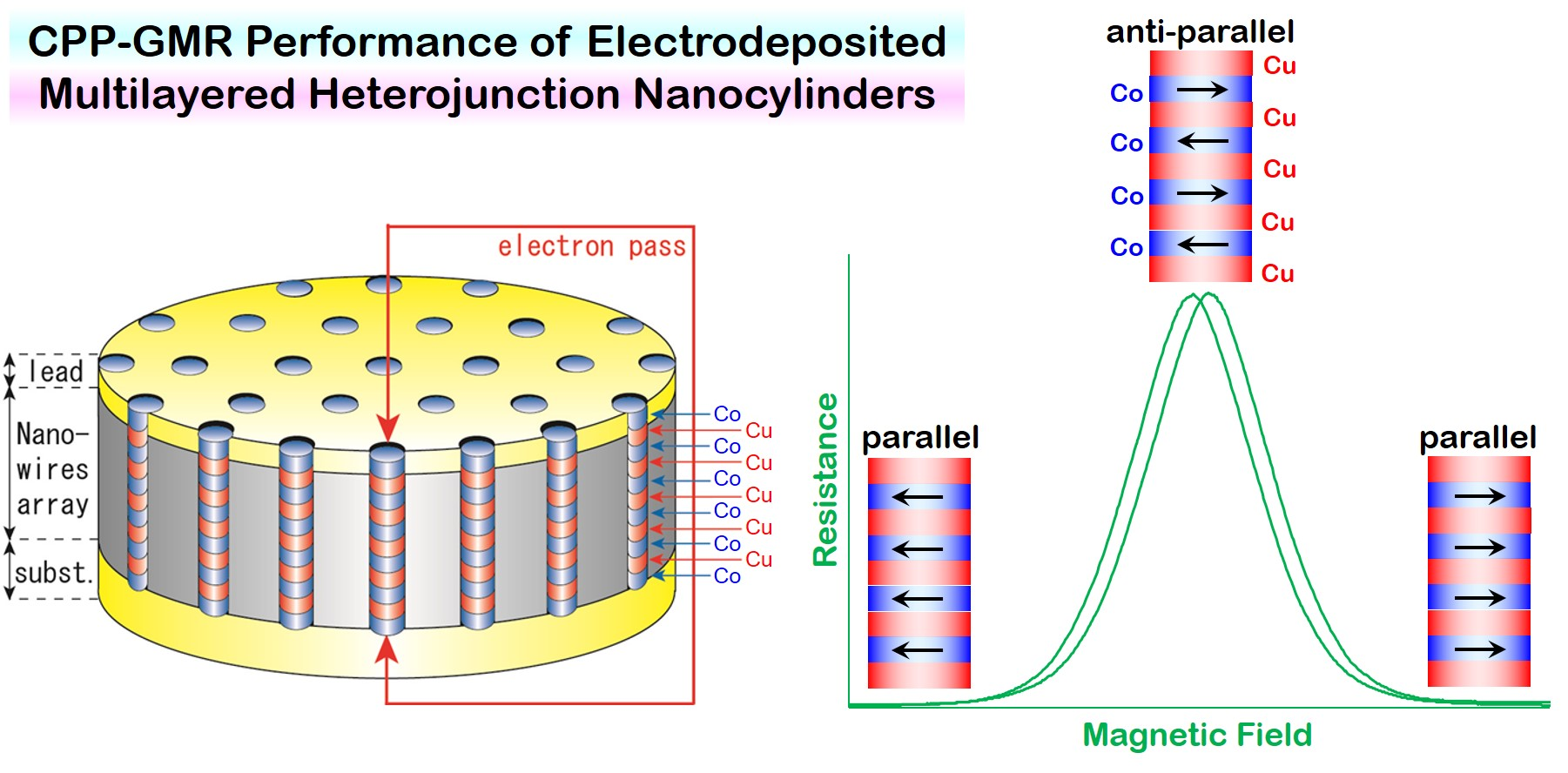
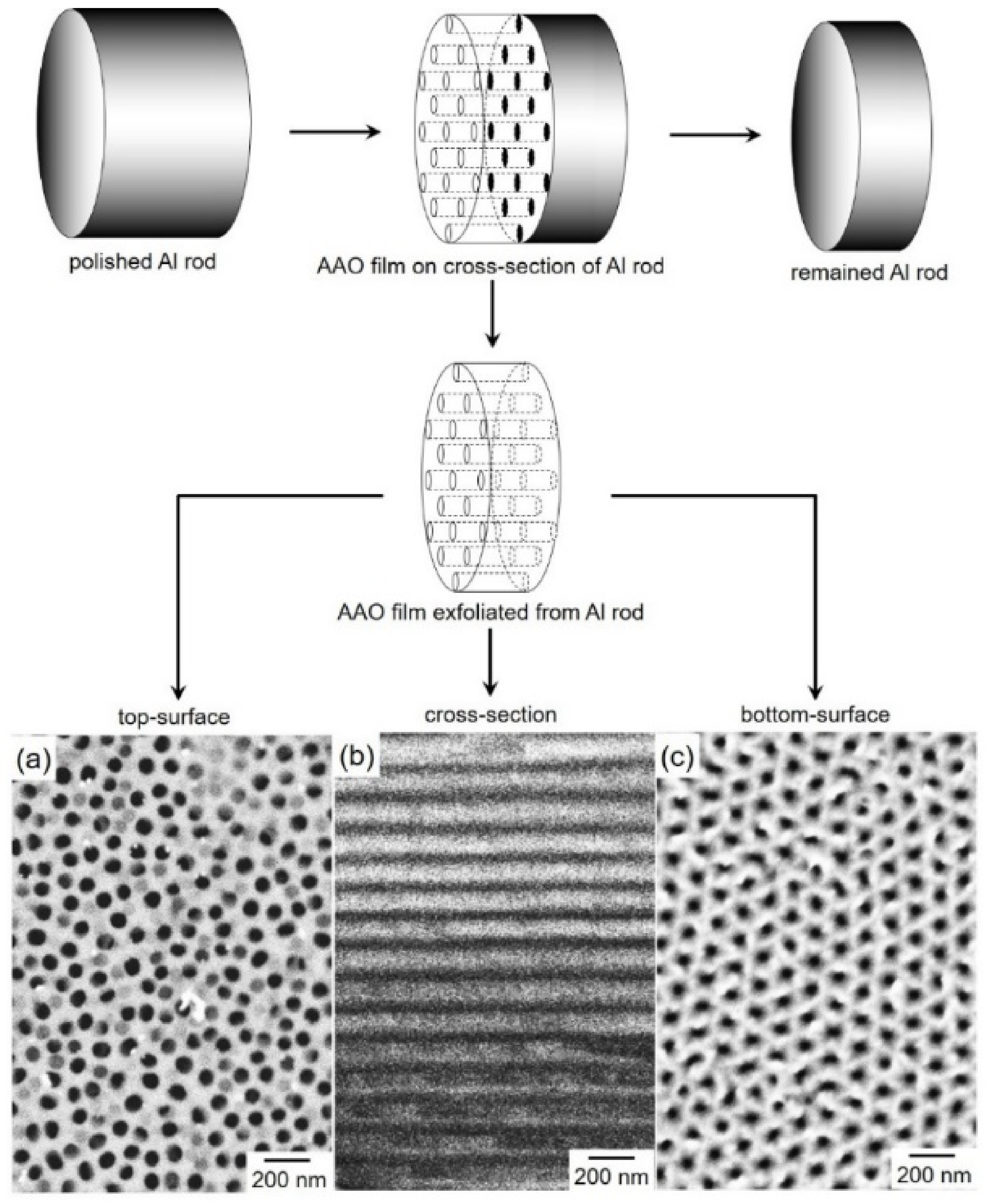
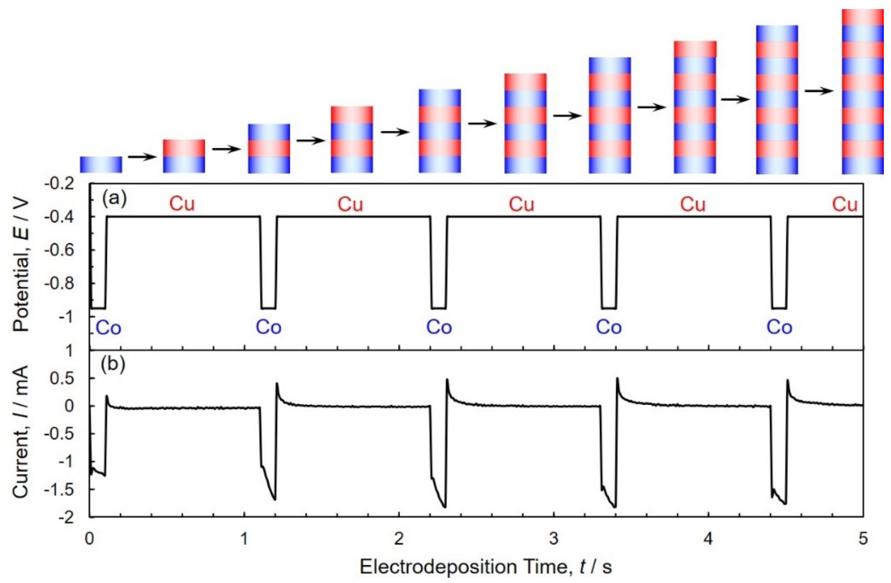
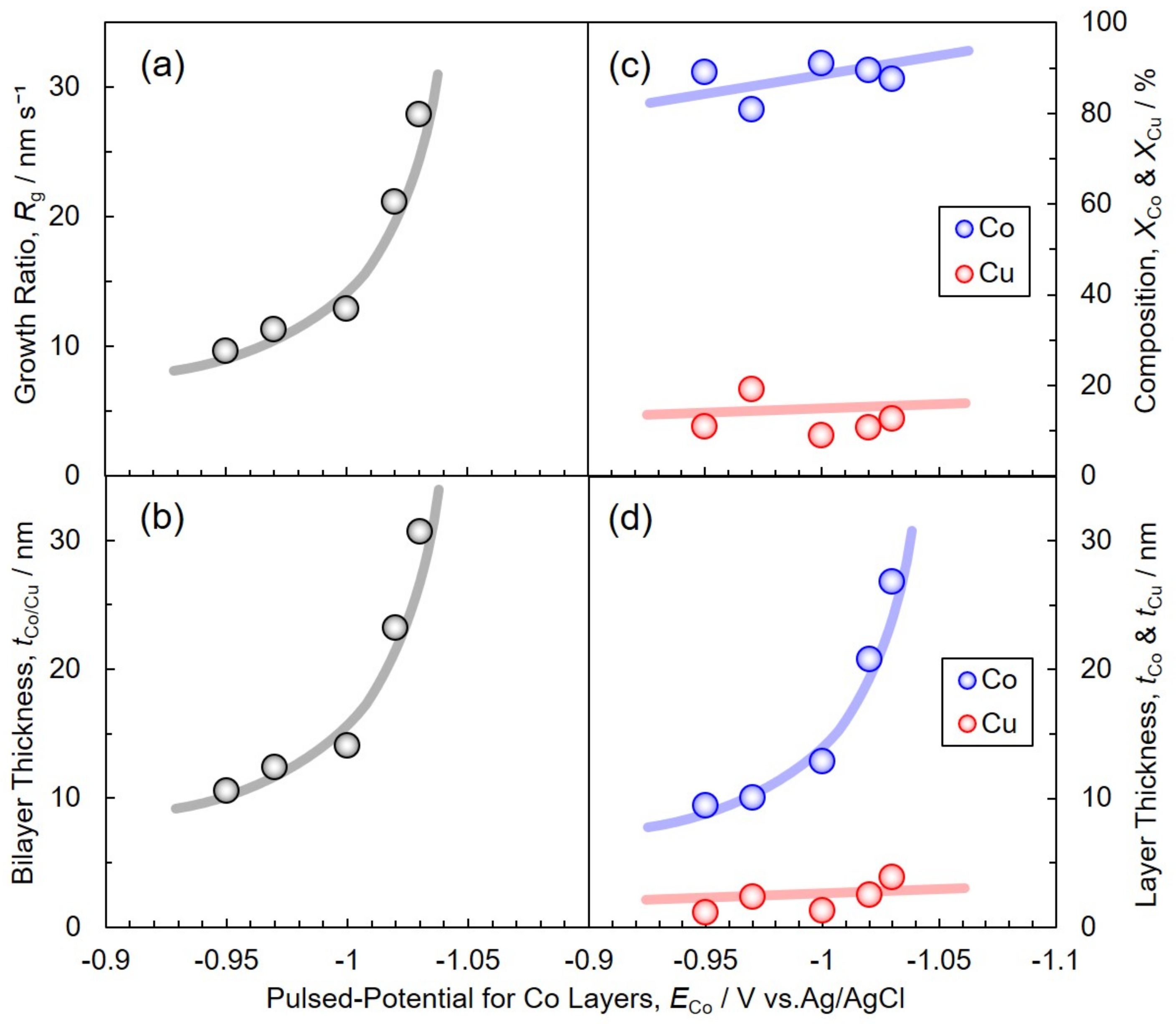
4.1. Template Synthesis and Electrodeposition Process of Co/Cu Heterojunction Nanocylinders

Figure 1 shows the FE-SEM images of the top-side view (Figure 1a), the cross-sectional view (Figure 1b), and the bottom-side view (Figure 1c) of an AAO nanochannel film that separated from a cross-section of an aluminum rod. The separated AAO film had an ideal nanochannel structure with ~50 nm in diameter. The nanochannel length, which is identical to the AAO film thickness, was ~60 µm.
Figure 2 shows the cathodic (blue line) and anodic (green and red lines) scanned polarization curves (Tafel slope) for Cu and Co electrodeposition from an aqueous solution containing Cu2+ and Co2+ ions. The Tafel plot was then employed to reveal the reduction behavior of Cu2+ ions by magnifying the relatively small current range. According to the Nernst equation, ECueq for Cu/Cu2+ is estimated to be +0.07 V vs. Ag/AgCl, while ECoeq for Co/Co2+ is also calculated to be −0.48 V vs. Ag/AgCl, as follow by Equation (10).
E e q = E 0 + R T n F ln M n +
Here, Eeq and E0 are the equilibrium potential and standard potential, respectively. R, F, n, and T are gas constant, Faraday constant, ionic valence, and absolute temperature, respectively. [Mn+] is the activity of the metal ions. As shown in Figure 2 (cathodic scan: blue line), the cathode current density starts to rise at +0.07 V, which is close to ECueq. It is well known that the normal metal ions, such as Cu2+, Sn2+, Zn2+ ions are immediately reduced to the metallic state without substantial overvoltage in an acidic aqueous solution [24]. Hence, this cathode current rising results from Cu2+ ions’ reduction.
The cathode potential significantly polarizes to −0.80 V at the current density of around 23 A m−2. In the range of current density, Cu2+ ions seem to reach a diffusion limit. Moreover, an increase in the cathode current density can be observed at −0.80 V, which is quite less noble than ECoeq. It is well-known that Co2+ ions are reduced to a metallic state, accompanying a substantial overvoltage owing to the multi-step reduction process, which was reported by Bockris et al. [25]. Furthermore, in the potential region less noble than −1.2 V, the current density reached over 1000 A m−2, and the cathode potential polarized significantly due to the diffusion limit of Co2+ ions [26]. On the contrary, in the anodic scan (green and red lines), the anodic current was observed at −0.13 V. This current seems to be caused by the dissolution of electrodeposited Co. For the pulsed potential deposition of Co/Cu multilayers, the suitable cathode potential for Cu layer, ECu should be less nobler than ECueq (+0.07 V) and initial dissolution potential for Co (−0.13 V). Additionally, ECu should be nobler than ECoeq (−0.48 V) to avoid Co contamination. Hence, in the present study, ECu was fixed to −0.4 V, while the suitable cathode potential for Co layer, ECo should be less nobler than ECoeq (−0.48 V) and initial deposition potential for Co (−0.80 V). To prevent Cu contamination, quite less nobler potential than −0.80 V is desirable for Co deposition. Moreover, ECo should be nobler than the diffusion limit potential for Co2+ ions (−1.2 V). In this study, Co layer thickness should be controlled within the several tens of nanometer range to investigate the spin-diffusion length based on the Valet–Fert equation. Therefore, ECo was determined to the range from −0.95 V~−1.03 V.
As shown in Figure 3, we synthesized Co/Cu multilayered nanocylinders by switching the cathode potential from −0.4 V (for 1.0 s) to −0.95 V~−1.03 V (for 0.1 s) to adjust the thickness of each layer within several nanometer scale. When the nanocylinders reached the Au thin layer on an AAO template, the reduction current was suddenly enhanced due to the in-situ electric contact with the Au thin layer and formation of hemispheric metal caps as shown in Figure 4. The time for filling AAO nanochannels with Co/Cu multilayered nanocylinders, TF, was determined from the time-dependence of observed current at the wide range of pulsed-potential deposition time as shown in Figure 4.
The growth rate of Co/Cu multilayered nanocylinders, Rg, can be estimated from dividing the AAO nanochannel’s length, L, by the filling time, TF. Furthermore, Co/Cu bilayer thickness, tCo/Cu, can be also estimated from the following Equation (11).
t C o / C u = L T C o + T C u T F
Here, TCo and TCu are the pulse-deposition time for each Co and Cu layer, respectively. In the present study, TCo and TCu correspond to 0.1 s and 1.0 s, respectively.
Figure 5a,b show the effect of ECo (pulsed potential for Co layer deposition) on the nanocylinder growth rate, Rg and Co/Cu bilayer thickness, tCo/Cu, respectively. When ECo was shifted to the less noble region, Rg and tCo/Cu increased logarithmically up to 27.9 nm s−1 and 30.7 nm, respectively. Based on Tafel equation (η = a + blogi), the overpotential, η, is proportional to the logarithm of current, logi, when the charge transfer process controls the electrochemical reaction. It is well-known that the nanocylinder growth rate and bilayer thickness are a linear relationship with the electrodeposition current density based on Faraday’s laws of electrolysis. Hence, Rg and tCo/Cu should be increased logarithmically with increasing the overpotential. The composition of Co, XCo and that of Cu, XCu in each sample were also determined from EDX analysis (EDX-800HS, Shimadzu, Kyoto, Japan) as shown in Figure 5c. All over the potential range from −0.95 V to −1.03 V, the average XCo and XCu were 87.58% and 12.42%, respectively. The compositions were also investigated by FE-SEM-EDS analysis (JSM-7500FA, JEOL, Tokyo, Japan). The average XCo and XCu were also determined to 87.96% and 12.04%, respectively. If the Cu impurities in Co layers are negligible, each average layer thickness of Co and Cu, tCo and tCu, can be estimated from the following Equations (12) and (13), respectively.
t C o = t C o / C u X C o 100
t C u = t C o / C u X C u 100
The effect of ECo on tCo and tCu is shown in Figure 5d. The tCu was almost constant at less than 4 nm all over the potential range. On the other hand, tCo became thicker as ECo was shifted to a less noble region. According to the above results, it was revealed that tCo can be controlled within the range from 8 to 27 nm by tuning ECo.

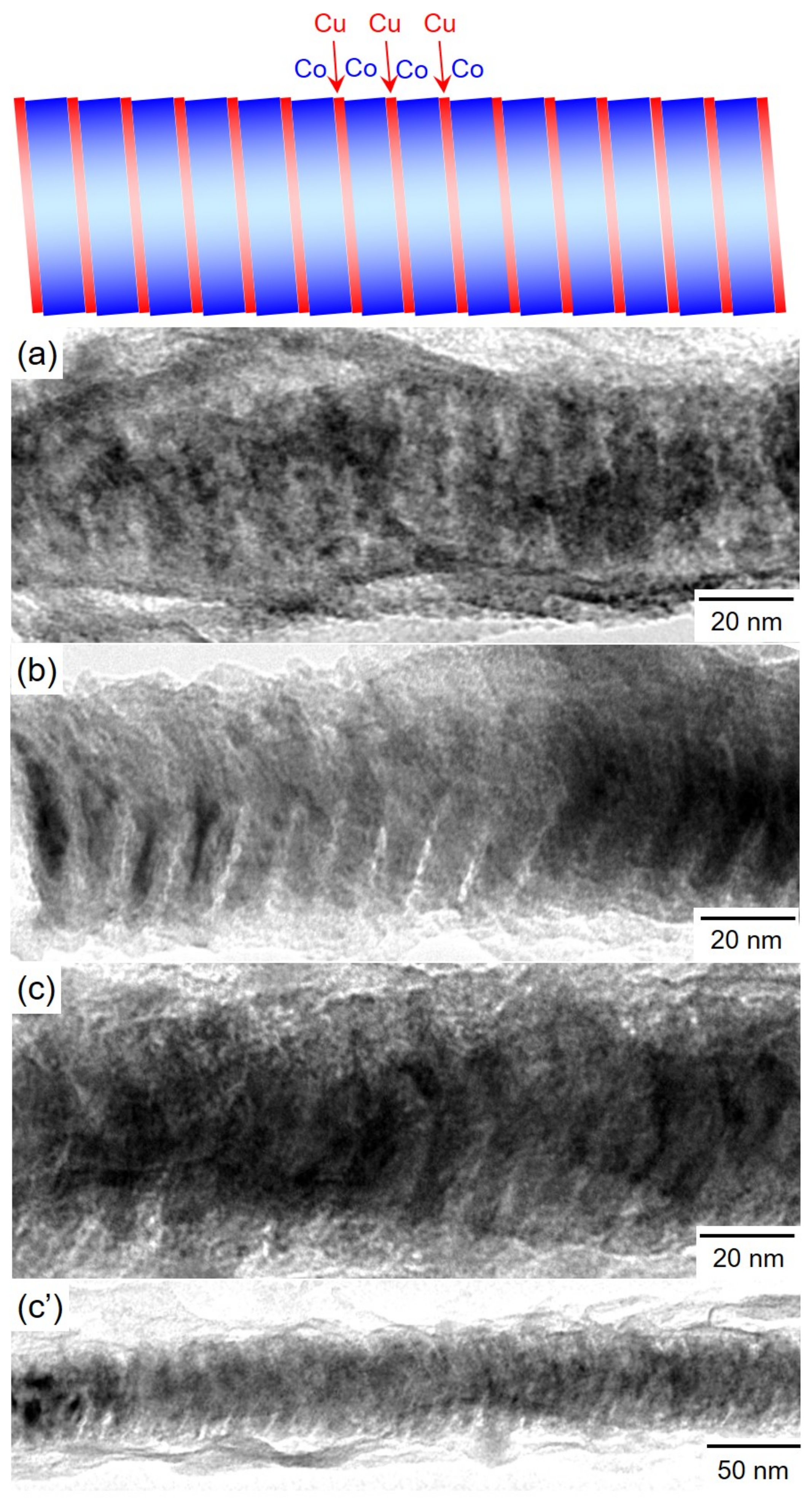
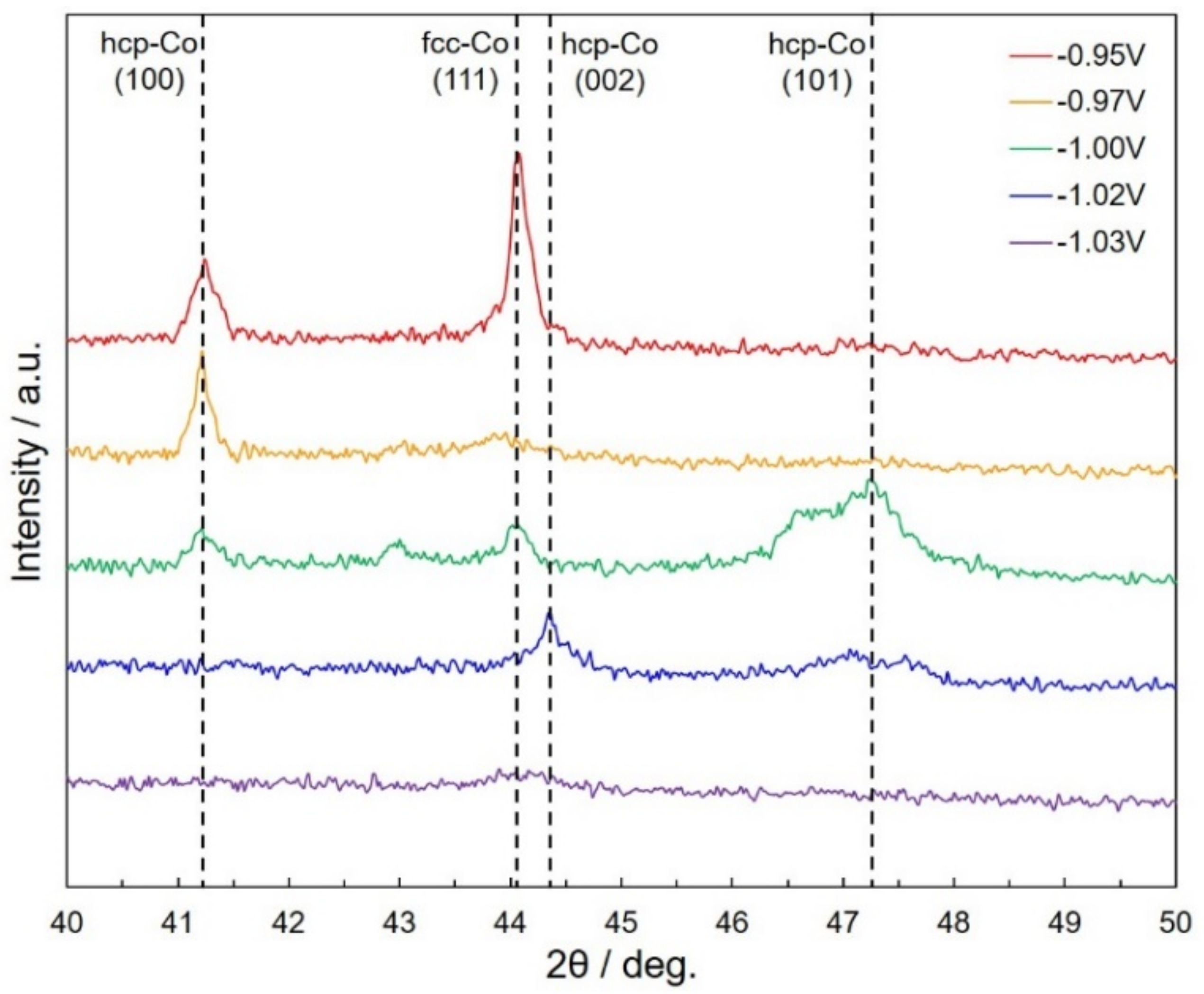
4.2. Structure of Co/Cu Heterojunction Nanocylinders

Figure 6 shows TEM bright-field images of Co/Cu multilayered nanocylinders. The samples were prepared by ranging the pulsed-potential for Co layer, ECo as the following: Figure 6a ECo = −0.95 V, Figure 6b ECo = −0.97 V and Figure 6c,c’ ECo = −1.00 V. While the other parameters: TCo, ECu and TCu were fixed to 0.1 s, −0.40 V and 1.0 s, respectively. The Co/Cu multilayered nanocylinders were separated from AAO templates. As shown in Figure 6, the diameter of Co/Cu multilayered nanocylinder is ~50 nm, which is almost identical to the diameter of AAO nanochannels as shown in Figure 1. The nanocylinder also has a multilayered heterojunction structure. The layer thickness of a dark thick layer is ~10 nm while that of a light thin layer is ~2 nm. The thick and thin layers correspond to the Co and Cu layers, respectively, considering the estimated layer thickness, as shown in Figure 5d.
Figure 7 renders the effect of ECo on the XRD profiles of Co/Cu multilayered nanocylinders. As shown in Figure 7, the observed peaks at 2θ = 41.25°, 44.1°, 44.4°, and 47.25° are derived from hcp-Co (100), fcc-Co (111), hcp-Co (002), and hcp-Co (101), respectively. The diffraction peak, which is derived from fcc-Co, is observed at 2θ = 44.1°. The presence of fcc-Co could be caused by the phase transformation from the hcp to the fcc structure because a part of the Co layer seems to contain Cu as the impurity element. Other researchers have also reported that the fcc-Co phase existed in the X-ray diffraction pattern on their Co/Cu multilayered films [27]. In contrast, the diffraction peak of fcc-Co disappeared when the pulsed potential for Co layer was set to a less nobler region. The peak disappearance results from an increase in the Co layer thickness, as shown in Figure 5d.

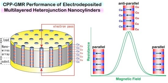
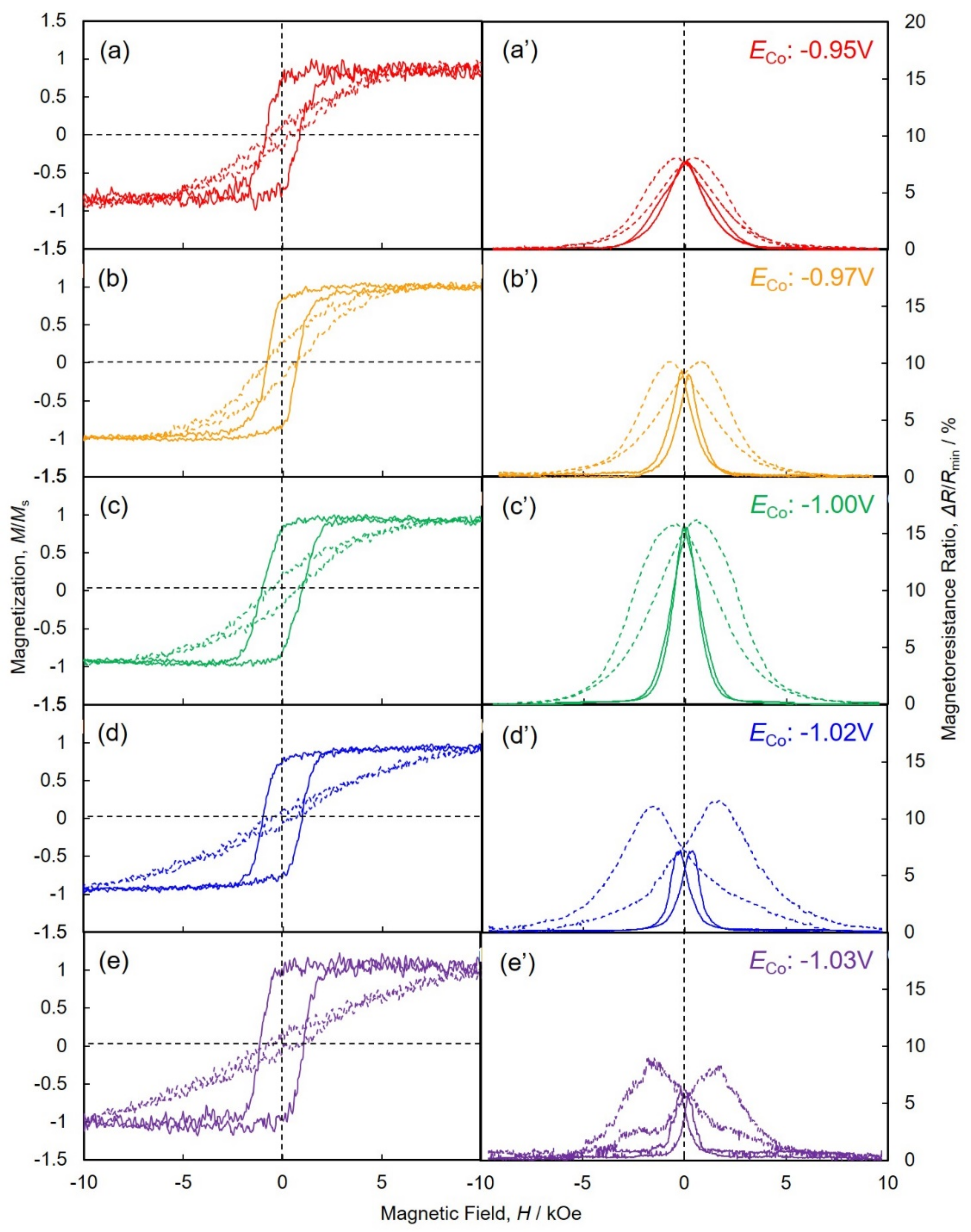
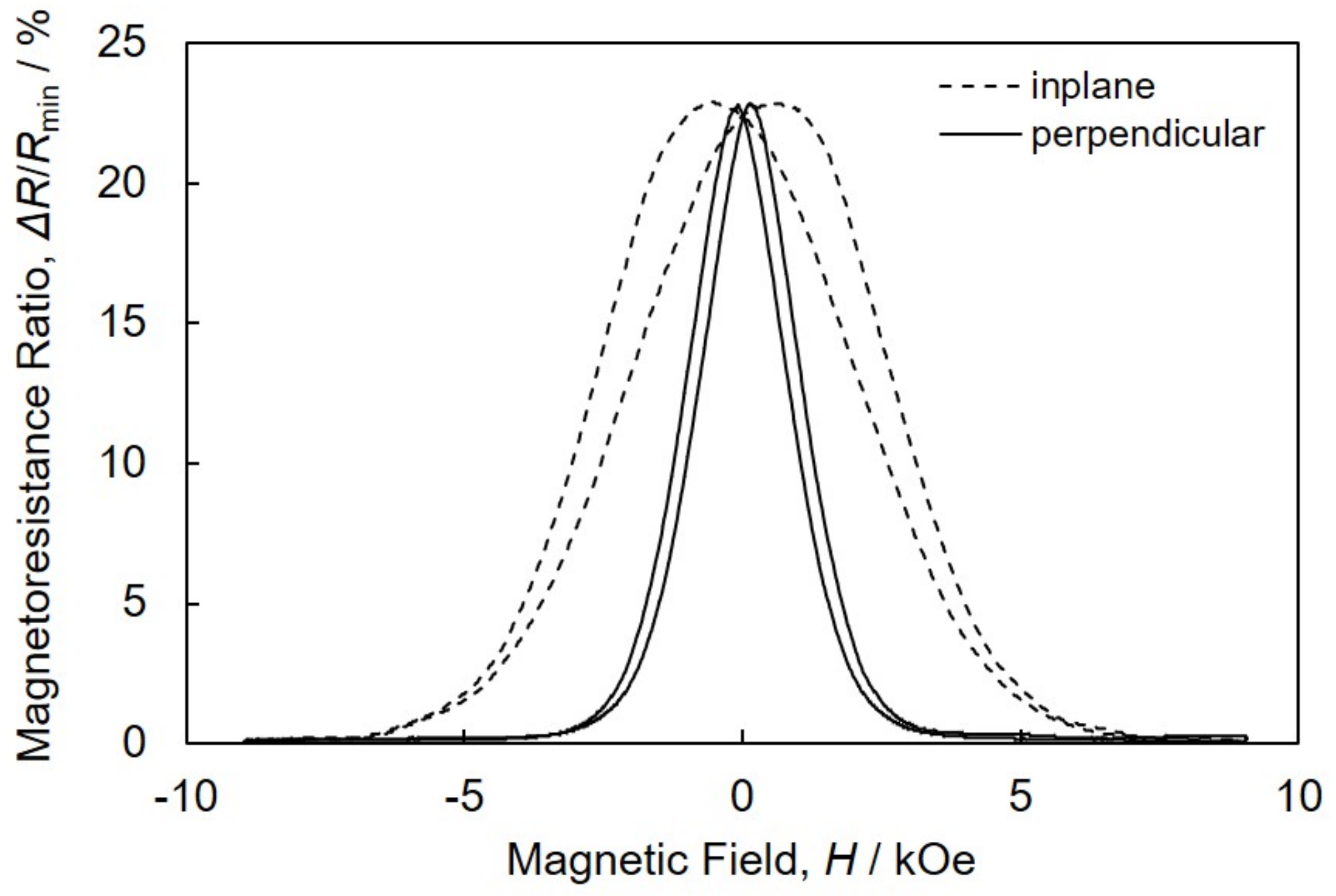
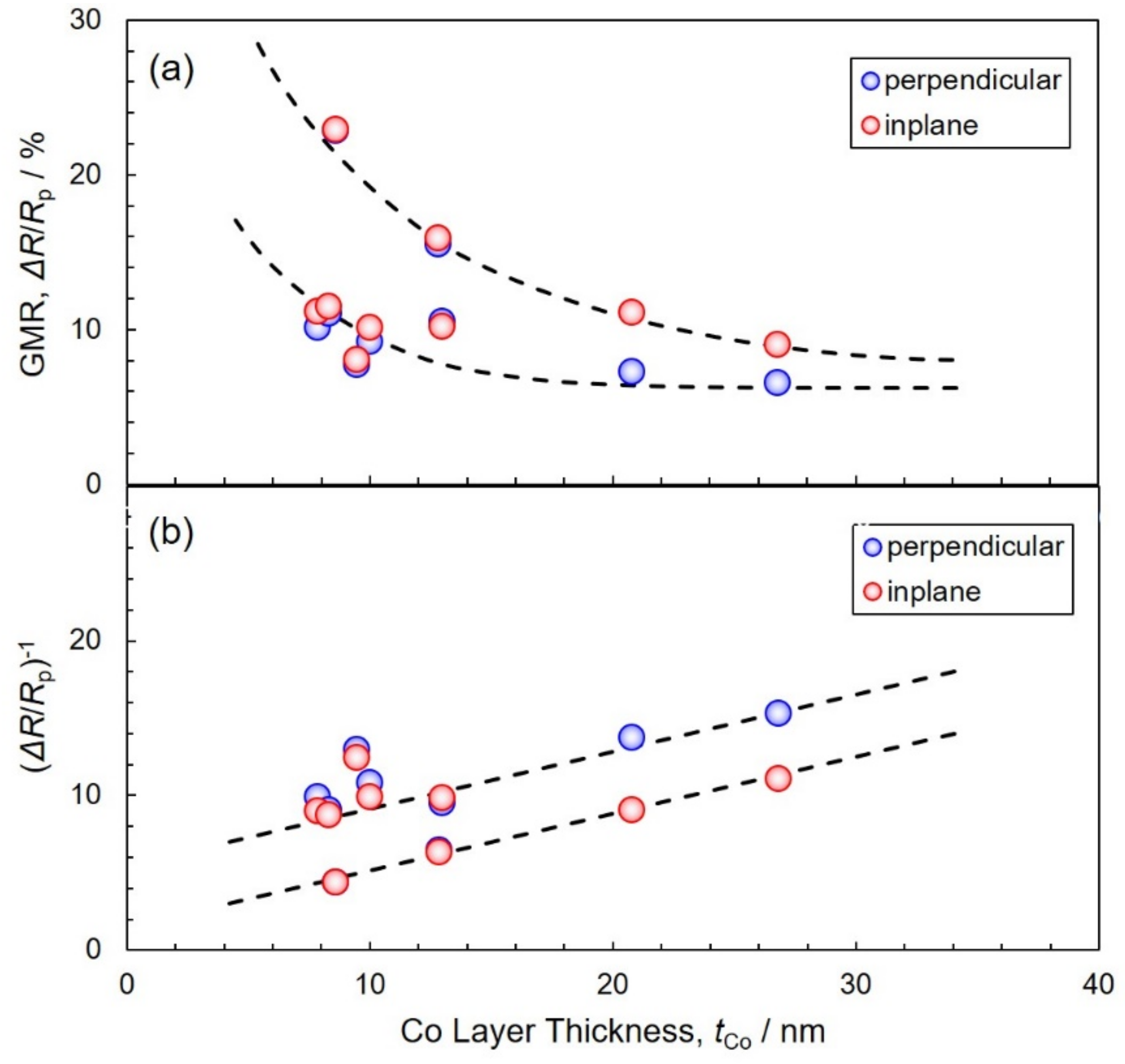
4.3. Magnetoresistance Properties of Co/Cu Multilayered Heterojunction Nanocylinders

The effect of ECo on the magnetic and magnetoresistance hysteresis curves of Co/Cu multilayered nanocylinder arrays is shown in Figure 8. The hysteresis curves, which were obtained in the magnetic field perpendicular to the AAO film, are plotted in the solid lines, while the curves that obtained in-plane direction are plotted in the dotted lines. As shown in the dotted lines of Figure 8a–d, it is quite difficult to achieve the saturation magnetization with a magnetic field in-plane direction to the AAO film due to a substantial demagnetizing field, Hd. The demagnetization factor, Nd with in-plane direction can be estimated to ~0.5. On the other hand, as shown by the solid lines, it is relatively easy to achieve the saturation magnetization with a perpendicular magnetic field to the AAO film plane. As shown in Equation (2), Hd will be minimal in a perpendicular direction, which corresponds to the axial direction of a nanocylinder. In this case, the external magnetic field will be effective and not reduced. Hence, the saturation magnetization can be realized by a small external magnetic field (~2 kOe) in the long axis direction of nanocylinders [28].
If the resistance of a multilayered structure can be expressed by the linear relationship with the composition, the resistance of a Co/Cu multilayered nanocylinder can be defined using the resistivities of a Co layer and a Cu layer as shown in Equation (14).
R = ρ C o X C o 100 + ρ C u X C u 100 L S
Here, R is the resistance of a Co/Cu nanocylinder. ρCo and ρCu are the resistivity of a Co layer (64.2 Ω/nm) and a Cu layer (16.8 Ω/nm), respectively. L and S are the length (60 µm) and the cross-section area (~6360 nm2) of a nanocylinder, respectively. According to Equation (14), R will increase with increasing XCo because ρCo is larger than ρCu. Based on our experimental results, the resistance of a Co/Cu multilayered nanocylinder, which was synthesized by an electrochemical in situ contact process, corresponded to the estimated value for the parallel contacts with only 1~3 nanocylinders regardless of the composition.
As shown by the dotted lines of Figure 8a–d, the magnetoresistance of Co/Cu multilayered nanocylinder arrays decreased like a Gaussian curve. The resistance reached the minimum in the range more than ~7 kOe as the magnetic field increased slowly in the in-plane (parallel) direction. On the other hand, the magnetoresistance ratio decreased quickly and reached zero at ~2 kOe with an increasing magnetic field in the perpendicular (axial) direction, as shown by the solid lines.
The GMR value of Co/Cu multilayered nanocylinder arrays, which were electrodeposited at ECo of −1.03 V, was ~9%, as shown in Figure 8e’. While, the GMR value of the nanocylinder arrays, which were electrodeposited at ECo of −1.00 V, increased up to ~16%, as shown in Figure 8c’. It has been reported that the GMR value increases as the number of interfaces between ferromagnetic and non-magnetic layers increases [29]. As shown in Figure 5d, the Co layer thickness became thinner as the pulsed potential was shifted to a noble region. This decrease in the Co layer thickness increases the number of layer interfaces. Hence, this increase in GMR seems to be caused by decreases in the Co layer thickness. For further improving the CPP-GMR performance, the Co layer thickness, tCo was decreased by shortening the pulse-deposition time for Co layer, TCo. To maintain the throwing power for the pulse-deposition, the pulsed-potential for Co layer, ECo was kept to less nobler than −1.03 V. Figure 9 show the magnetoresistance hysteresis loops of an AAO nanochannel film with Co/Cu multilayered nanocylinder arrays. The nanocylinder arrays were electrodeposited using the pulse parameters of ECo = −1.05 V, TCo = 0.03 s, ECu = −0.4 V and TCu = 1.0 s. As shown in Figure 9, the CPP-GMR value reached up to ca. 23% in the Co/Cu multilayered nanocylinder with 8.6 nm in tCo and 4 nm in tCu.
Table 1 shows the summary of CPP-GMR performances (at room temperature) of electrodeposited multilayered nanocylinders that were reported by the other researchers. Most researchers have reported that the CPP-GMR value reached up to ca. 15~20% at room temperature in the tCo range from ca. 5 to 20 nm and the tCu range from ca. 5 to 10 nm. Those values give good agreement with the value obtained in the present study.
Figure 10 shows the effect of Co layer thickness on the GMR value and (ΔR/Rp)−1 of Co/Cu multilayered nanocylinders. As shown in Figure 10a, the GMR value increases with a decreasing Co layer thickness. In the Co layer thickness of 8.6 nm, the GMR value reached up to ~23%. As shown in Figure 10b, with a decrease in the thickness of the Co layer, (ΔR/Rp)−1 decreases linearly [13]. This tendency corresponds well to Valet–Fert Equation (8). The spin-diffusion length of magnetic metal can also be estimated from the slope of approximate expression in Figure 10b. Consequently, the cobalt spin-diffusion length, lCosf, was estimated to be ~12.5 nm. As the thickness of the Co layer, tCo, is from 8 to 27 nm, the condition of tF > lFsf in the Valet–Fert model seems to be satisfied by the results in the present study.

5. Conclusions

AAO nanochannel films (D: ~50 nm, L: ~60 µm) were fabricated using an anodization and exfoliation technique from a metallic aluminum rod. The Co/Cu multilayered nanocylinders were fabricated by alternating the cathode potentials for Cu and Co deposition to adjust the Co layer thickness within ~30 nm. From the TEM images of the Co/Cu multilayered nanocylinders, it was confirmed that the Co and Cu layers were alternately laminated, and the diameter of the nanocylinders was the same as the pore diameter of the AAO template. The multilayered nanocylinders with alternating Cu and Co layers contained both hcp and fcc phases of cobalt. The multilayered nanocylinders with alternating Cu and Co layers reached saturation magnetization with a small magnetic field (~2 kOe) in the axial direction of nanocylinders due to the substantial aspect ratio. As the Co layer thickness decreased, the GMR reached up to approx. 23%. When decreasing the Co layer thickness, (ΔR/Rp)−1 linearly decreased according to the Valet–Fert equation; this can be explained under the condition of tF > lFsf and tN < lNsf. The cobalt spin-diffusion length, lCosf, was estimated to be ~12.5 nm by the slope of approximate expression.

Author Contributions

S.M. and M.H. carried out experiments, analyzed data, and wrote the manuscript; T.O. designed the study, supervised the project, and analyzed data. All authors have read and agreed to the published version of the manuscript.

Funding

This research was funded by the Japan Society for the Promotion of Science, grant number 18H01754.

Institutional Review Board Statement

Not applicable.

Informed Consent Statement

Not applicable.

Acknowledgments

The authors acknowledge financial support from the Japan Society for the Promotion of Science.

Conflicts of Interest

The authors declare that they have no competing interests.

References

  1. Baibich, M.N.; Broto, J.M.; Fert, A.; Nguyen, V.D.F.; Petroff, F. Giant Magnetoresistance of (001)Fe/(001)Cr Magnetic Super-Lattices. Phys. Rev. Lett. 1988, 61, 2472–2475. [Google Scholar] [CrossRef] [PubMed] [Green Version]
  2. Binasch, G.; Grünberg, P.; Saurenbach, F.; Zinn, W. Enhanced Magnetoresistance in Fe-Cr Layered Structures with Antiferro-Magnetic Interlayer Exchange. Phys. Rev. B 1989, 39, 4828. [Google Scholar] [CrossRef] [PubMed] [Green Version]
  3. Alper, M.; Attenborough, K.; Hart, R.; Lane, S.; Lashmore, D.S.; Younes, C.; Schwarzacher, W. Giant Magnetoresistance in Electrodeposited Superlattices. Appl. Phys. Lett. 1993, 63, 2144–2146. [Google Scholar] [CrossRef]
  4. Lenczowski, S.; Schönenberger, C.; Gijs, M.; De Jonge, W. Giant Magnetoresistance of Electrodeposited Co/Cu Multilayers. J. Magn. Magn. Mater. 1995, 148, 455–465. [Google Scholar] [CrossRef]
  5. Tóth, B.G.; Peter, L.; Dégi, J.; Revesz, A.; Oszetzky, D.; Molnár, G.; Bakonyi, I. Influence of Cu Deposition Potential on the Giant Magnetoresistance and Surface Roughness of Electrodeposited Ni–Co/Cu Multilayers. Electrochim. Acta 2013, 91, 122–129. [Google Scholar] [CrossRef] [Green Version]
  6. Sahin, T.; Kockar, H.; Alper, M. Properties of Electrodeposited CoFe/Cu Multilayers: The Effect of Cu Layer Thickness. J. Magn. Magn. Mater. 2015, 373, 128–131. [Google Scholar] [CrossRef]
  7. Zsurzsa, S.; Peter, L.; Kiss, L.; Bakonyi, I. Magnetic and Magnetoresistance Studies of Nanometric Electrodeposited Co Films and Co/Cu Layered Structures: Influence of Magnetic Layer Thickness. J. Magn. Magn. Mater. 2017, 421, 194–206. [Google Scholar] [CrossRef] [Green Version]
  8. Piraux, L.; George, J.-M.; Despres, J.F.; Leroy, C.; Ferain, E.; Legras, R.; Ounadjela, K.; Fert, A. Giant Magnetoresistance in Magnetic Multilayered Nanowires. Appl. Phys. Lett. 1994, 65, 2484–2486. [Google Scholar] [CrossRef]
  9. Blondel, A.; Meier, J.P.; Doudin, B.; Ansermet, J. Giant Magnetoresistance of Nanowires of Multilayers. Appl. Phys. Lett. 1994, 65, 3019–3021. [Google Scholar] [CrossRef]
  10. Evans, P.R.; Yi, G.; Schwarzacher, W. Current Perpendicular to Plane Giant Magnetoresistance of Multilayered Nanowires Electrodeposited in Anodic Aluminum Oxide Membranes. Appl. Phys. Lett. 2000, 76, 481–483. [Google Scholar] [CrossRef]
  11. Ohgai, T.; Hoffer, X.; Gravier, L.; Ansermet, J.P. Electrochemical Surface Modification of Aluminium Sheets for Application to Nano-Electronic Devices: Anodization Alminium and Cobalt-Copper Electrodeposition. J. Appl. Electrochem. 2004, 34, 1007–1012. [Google Scholar] [CrossRef] [Green Version]
  12. Tang, X.-T.; Wang, G.-C.; Shima, M. Perpendicular Giant Magnetoresistance of Electrodeposited Co∕Cu-Multilayered Nanowires in Porous Alumina Templates. J. Appl. Phys. 2006, 99, 033906. [Google Scholar] [CrossRef] [Green Version]
  13. Tang, X.T.; Wang, G.C.; Shima, M. Layer Thickness Dependence of CPP Giant Magnetoresistance in Individual CoNi/Cu mul-tilayer Nanowire Grown by Electrodeposition. Phys. Rev. B 2007, 75, 134404. [Google Scholar] [CrossRef] [Green Version]
  14. Shakya, P.; Cox, B.; Davis, D. Giant Magnetoresistance and Coercivity of Electrodeposited Multilayered FeCoNi/Cu and CrFeCoNi/Cu. J. Magn. Magn. Mater. 2012, 324, 453–459. [Google Scholar] [CrossRef]
  15. Zhang, W.; Deng, H.; Li, H.; Su-Wei, Y.; Wang, H. Synthesis and Magnetic Properties of Ni–Fe/Cu/Co/Cu Multilayer Nanowire Arrays. J. Mater. Sci. Mater. Electron. 2015, 26, 2520–2524. [Google Scholar] [CrossRef]
  16. Han, J.; Qin, X.; Quan, Z.; Wang, L.; Xu, X. Perpendicular Giant Magnetoresistance and Magnetic Properties of Co/Cu Nan-Owire Arrays Affected by Period Number and Copper Layer Thickness. Adv. Condens. Matter Phys. 2016, 2016, 1–9. [Google Scholar] [CrossRef] [Green Version]
  17. Xi, H.; Gao, Y.; Liu, Z.; Han, G.; Lu, J.; Li, Y. Inter- and Intra-nanowire Magnetic Interaction in Co/Cu Multilayer Nanowires Deposited by Electrochemical Deposition. Phys. B Condens. Matter 2017, 518, 77–80. [Google Scholar] [CrossRef]
  18. Kamimura, H.; Hayashida, M.; Ohgai, T. CPP-GMR Performance of Electrochemically Synthesized Co/Cu Multilayered Nan-owire Arrays with Extremely Large Aspect Ratio. Nanomaterials 2020, 10, 5. [Google Scholar] [CrossRef] [Green Version]
  19. Lee, W.; Ji, R.; Gösele, U.; Nielsch, K. Fast Fabrication of Long-Range Ordered Porous Alumina Membranes by Hard Anodization. Nat. Mater. 2006, 5, 741–747. [Google Scholar] [CrossRef]
  20. Ohgai, T.; Mizumoto, M.; Nomura, S.; Kagawa, A. Electrochemical Fabrication of Metallic Nanowires and Metal Oxide na-Nopores. Mater. Manuf. Process. 2007, 22, 440–443. [Google Scholar] [CrossRef] [Green Version]
  21. Valet, T.; Fert, A. Theory of the Perpendicular Magnetoresistance in Magnetic Multilayers. Phys. Rev. B 1993, 48, 7099–7113. [Google Scholar] [CrossRef] [PubMed]
  22. Piraux, L.; Dubois, S.; Fert, A.; Belliard, L. The Temperature Dependence of the Perpendicular Giant Magnetoresistance in Co/Cu Multilayered Nanowires. Eur. Phys. J. B 1998, 4, 413–420. [Google Scholar] [CrossRef]
  23. Fert, A.; Piraux, L. Magnetic nanowires. J. Magn. Magn. Mater. 1999, 200, 338–358. [Google Scholar] [CrossRef]
  24. Nakano, H.; Ohgai, T.; Fukushima, H.; Akiyama, T.; Kammel, R. Factors Determining the Critical Current Density for Zinc Deposition in Sulfate Solutions. Metall 2001, 55, 676–681. [Google Scholar]
  25. Bockris, J.O.; Kita, H. Analysis of Galvanostatic Transients and Application to the Iron Electrode Reaction. J. Electrochem. Soc. 1961, 108, 676–685. [Google Scholar] [CrossRef]
  26. Ohgai, T.; Tanaka, Y.; Fujimaru, T. Soft Magnetic Properties of Ni-Cr and Co-Cr Alloy Thin Films Electrodeposited from Aqueous Solutions Containing Trivalent Chromium Ions and Glycine. J. Appl. Electrochem. 2012, 42, 893–899. [Google Scholar] [CrossRef] [Green Version]
  27. Rafaja, D.; Schimpf, C.; Klemm, V.; Schreiber, G.; Bakonyi, I.; Péter, L. Formation of Microstructural Defects in Electrodeposited Co/Cu Multilayers. Acta Mater. 2009, 57, 3211–3222. [Google Scholar] [CrossRef]
  28. Ohgai, T.; Washio, R.; Tanaka, Y. Anisotropic Magnetization Behavior of Electrodeposited Nanocrystalline Ni-Mo Alloy Thin Films and Nanowires Array. J. Electrochem. Soc. 2012, 159, H800–H804. [Google Scholar] [CrossRef] [Green Version]
  29. Dulal, S.; Charles, E. Effect of Interface Number on Giant Magnetoresistance. J. Phys. Chem. Solids 2010, 71, 309–313. [Google Scholar] [CrossRef]
Figure 1. FE-SEM images of top-view (a), cross-section (b), and bottom-view (c) of an anodized aluminum oxide nanochannel template which was exfoliated from the cross-section of an aluminum rod.
Nanomaterials 11 00218 g001
Figure 2. Cathodic (blue line) and anodic (green and red lines) scanned polarization curves (Tafel slope) for Cu and Co electrodeposition from an aqueous solution containing 0.5 M Co (SO3NH2)2·4H2O, 0.005 M CuSO4·5H2O and 0.4 M H3BO3.
Nanomaterials 11 00218 g002
Figure 3. Time-dependence of applied potential (a) and observed current (b) at the beginning of pulsed-potential deposition time for growing Co/Cu multilayered nanocylinders. The cathode potential was alternatingly changed between −0.4 V (1.0 s) and −0.95 V (0.1 s).
Nanomaterials 11 00218 g003
Figure 4. Schematic image for filling the AAO nanochannels with Co/Cu multilayered nanocylinders at the wide range of pulsed-potential deposition time.
Nanomaterials 11 00218 g004
Figure 5. Effects of pulsed-potential for Co layers, ECo, on the growth rate of nanocylinders, Rg (a), Co/Cu bilayer thickness, tCo/Cu (b), the average composition, XCo and XCu (c), and the average layer thickness, tCo and tCu (d). TCo, ECu and TCu were fixed to 0.1 s, −0.40 V and 1.0 s, respectively.
Nanomaterials 11 00218 g005
Figure 6. TEM images of Co/Cu multilayered nanocylinders that were separated from an anodized aluminum oxide nanochannel template. (a) ECo = −0.95 V, (b) ECo = −0.97 V, (c,c’) ECo = −1.00 V. TCo, ECu and TCu were fixed to 0.1 s, −0.40 V and 1.0 s, respectively.
Nanomaterials 11 00218 g006
Figure 7. Effect of pulsed-potential for Co layer, ECo on the X-ray diffractograms of Co/Cu multilayered nanocylinders. ECo was set for −0.95 V, −0.97 V, −1.00 V, −1.02 V and −1.03 V. TCo, ECu and TCu were fixed to 0.1 s, −0.40 V and 1.0 s, respectively.
Nanomaterials 11 00218 g007
Figure 8. Effect of pulsed-potential for Co layers, ECo on the magnetic and magnetoresistance hysteresis loops of AAO nanochannel films with Co/Cu multilayered nanocylinder arrays. ECo was set for −0.95 V (a,a’), −0.97 V (b,b’), −1.00 V (c,c’), −1.02 V (d,d’) and −1.03 V (e,e’). TCo, ECu and TCu were fixed to 0.1 s, −0.40 V and 1.0 s, respectively. The magnetic field was applied to in-plane (dotted lines) and perpendicular (solid lines) directions to the multilayer interfaces.
Nanomaterials 11 00218 g008
Figure 9. Magnetoresistance hysteresis loops of an AAO nanochannel film with Co/Cu multilayered nanocylinder arrays. The sample was synthesized using the pulse parameters of ECo = −1.05 V, TCo = 0.03 s, ECu = −0.4 V and TCu = 1.0 s. The magnetic field was applied to in-plane (dotted lines) and perpendicular (solid lines) directions to the multilayer interfaces.
Nanomaterials 11 00218 g009
Figure 10. Effect of Co layer thickness on GMR (a) and (ΔR/Rp)−1 (b) in electrodeposited Co/Cu multilayered nanocylinders.
Nanomaterials 11 00218 g010
Table 1. Summary of CPP-GMR performance (at room temperature) of multilayered nanocylinders electrodeposited into AAO that were reported by the other researchers. The nanocylinders in Refs. [8,9] were electrodeposited into ion-track-etched polycarbonate membranes.
AuthorsFM/NMGMR/%D/nmL/μmL/DtCo/nmtCu/nmSource TitleYearRef.
Piraux et al.Co/Cu1540102501010Appl. Phys. Lett.1994[8]
Blondel et al.Co/Cu148067555Appl. Phys. Lett.1994[9]
Evans et al.CoNi/Cu553006020052Appl. Phys. Lett.2000[10]
Ohgai et al.Co/Cu15602331010J. Appl. Electrochem.2004[11]
Tang et al.Co/Cu1430060200810J. Appl. Phys.2006[12]
Tang et al.CoNi/Cu2330060200104Phys. Rev. B2007[13]
Shakya et al.FeCoNi/Cu15300602001410J. Magn. Magn. Mater2012[14]
Zhang et al.FeNi/Cu/Co451202172515J. Mater. Sci. M. E.2015[15]
Han et al.Co/Cu135011220505Adv. Cond. Mat. Phys.2016[16]
Xi et al.Co/Cu0.16803382005Physica B2017[17]
Kamimura et al.Co/Cu247570933191.4Nanomaterials2020[18]
Publisher’s Note: MDPI stays neutral with regard to jurisdictional claims in published maps and institutional affiliations.

