Abstract
The electrical characteristics of Zinc oxide (ZnO) thin-film transistors are analyzed to apprehend the effects of oxygen vacancies after vacuum treatment. The energy level of the oxygen vacancies was found to be located near the conduction band of ZnO, which contributed to the increase in drain current (ID) via trap-assisted tunneling when the gate voltage (VG) is lower than the specific voltage associated with the trap level. The oxygen vacancies were successfully passivated after the annealing of ZnO in oxygen ambient. We determined that the trap-induced Schottky barrier lowering reduced a drain barrier when the drain was subjected to negative bias stress. Consequentially, the field effect mobility increased from 8.5 m2 V−1·s−1 to 8.9 m2 V−1·s−1 and on-current increased by ~13%.
1. Introduction
Zinc oxide (ZnO) is an amorphous oxide semiconductor that can be economically patterned via simple wet chemical etching at low temperatures. ZnO has several favorable properties such as nontoxicity, flexibility and transparency [1,2,3,4]. Owing to these benefits, ZnO was extensively studied for applications in various thin-film devices such as nanogenerators, thermal and pressure sensors, flexible devices, memory devices and logical circuits.
In particular, ZnO was investigated as a promising alternative to the polysilicon channel materials used in backplane thin-film transistors (TFTs) because of its high mobility ~20 cm2 V−1∙s−1 [5,6]. Various composite materials containing ZnO such as InGaZnO and InSnZnO have also been studied for this application [7,8,9]. In general, the electrical characteristics of TFTs, having an amorphous oxide semiconductor channel including ZnO, show a strong ambient dependence during the fabrication process [10] and electrical operation [11,12], which were attributed to the various oxygen vacancies such as VO, VO+ and VO2+. These oxygen vacancies can exist at different energy levels: VO at 0.4 eV from the valence band, VO+ at 2.56 eV from the valence band and VO2+ at 3.2 eV from the valence band [13,14]. These oxygen vacancies serve as active trap sites and cause various reliability problems [15,16,17]. Although several countermeasures for this problem have been developed using passivation layers such as SiO2 and HfO2 [18,19], the detailed mechanisms of device degradation and recovery related with the oxygen vacancies have not been systematically investigated.
In this study, the non-passivated ZnO TFTs were fabricated using atomic layer deposition (ALD) and the influences of various oxygen treatments and field stress were investigated to determine the correlation between the electrical characteristics and the oxygen vacancies. The energy level of reversible oxygen vacancies in ZnO was found to be near the conduction band. Furthermore, we observed that the field–effect mobility and on-current were increased by a trap-induced Schottky barrier lowering after the drain was subjected to negative bias stress [20].
2. Materials and Methods
For back gate device fabrication, SiO2 (90 nm)/highly p-doped silicon substrate (resistivity < 0.005 Ω cm) was first cleaned in SC1 solution (NH4OH:H2O2:H2O = 1:1:5 at 80 °C for 10 min). Then, 50-nm-thick ZnO was deposited using ALD with 300 cycles of DEZ (0.2 s)/N2 purge (10 s)/H2O (0.6 s)/N2 purge (10 s) at 120 °C. ZnO channel was then patterned using photolithography and diluted HCl etchant. Finally, Au source and drain electrodes were deposited by an e-beam evaporator that was 100-nm-thick and patterned via photolithography and metal wet etching process. The SEM image of ZnO TFTs and the schematic of the device structure are shown in Figure 1a. The quality of ZnO was verified by Raman spectroscopy (514 nm) and a typical Raman peak of ZnO was observed at ~433 cm−1 [21] as shown in Figure 1b.
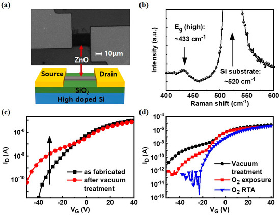
Figure 1.
(a) SEM image of back gate ZnO thin-film transistors (TFT) and the schematic of the device structure. Channel width and length are 25 μm and 30 μm, respectively; (b) Raman spectrum of ZnO channel showing ZnO related peak at ~433 cm−1; (c) representative transfer curves before (black) and after (red) the vacuum treatment at ~10−3 Torr for 24 h; (d) transfer curves after different treatments: Black circle line denotes the effect of low vacuum treatment; the red square, the sample exposed to oxygen atmosphere at 1 bar pressure and room temperature (25 °C) for 24 h; blue triangle, the effect of a rapid thermal annealing (RTA) system at 150 °C for 30 min, where the oxygen flow was maintained at 500 sccm.
In order to analyze the effect of oxygen vacancies, three different treatments were used. First, three samples were stored in a vacuum chamber (~10−3 Torr, 24 h) to intentionally create oxygen vacancies. One of them was then exposed to oxygen for 24 h (1 bar, 30 °C) to reduce the oxygen vacancies. The next sample was annealed in oxygen atmosphere using rapid thermal annealing (RTA) process (30 min, 150 °C, 500 sccm) to accelerate the reduction of oxygen vacancies. The annealing temperature, 150 °C, was deliberately selected to be slightly above the deposition temperature to make this process compatible with flexible electronics (<200 °C).
The electrical characteristics were measured at 30 °C in ambient air. For detailed device characterization, the following assessments were performed: (i) Reliability assessments to determine the effect of the increased oxygen vacancies after vacuum treatment on the Schottky barrier; (ii) The ZnO TFTs stored in vacuum were subjected to a negative drain bias stress, to investigate the degradation of the Schottky barrier (VD.stress = −2.5 V, VG.stress = 0 V); (iii) The effect of stress on the channel/drain junction was investigated by measuring the ID–VG transfer curve and the capacitance between the source and the drain.
The ID–VG measurement and stress application were performed using stress and measurement method of Keithley 4200-SCS parameter analyzer and the delay between the stress and measurement was less than a few tens of a millisecond. Capacitance–voltage curves were measured using an Agilent 4294A impedance analyzer.
3. Results and Discussions
ZnO TFTs with an Au electrode showed n-type device characteristics as shown in Figure 1c. The field-effect mobility extracted from the as fabricated device shown in Figure 1c was approximately 10 cm2/V∙s, which is similar to the values reported in the literature [22,23]. Field-effect mobility was calculated using μFE = (L/W ∙ Cox ∙ VD) (∂ID/∂VG). After the vacuum treatment, a “hump” (red line) was observed at the low field region of ID and the Ioff increased by three orders of magnitude from 3.1 × 10⁻¹² A to 2.8 × 10⁻⁹ A at VG = −40 V. When the ZnO TFTs were exposed to the oxygen ambient at 1 bar for 24 h at 30 °C, the hump was reduced primarily at the subthreshold region as shown in Figure 1d. When the ZnO TFTs were annealed at 150 °C for 10 min in oxygen ambient, the hump at the subthreshold region almost disappeared, indicating that the hump at the subthreshold region is due to the oxygen vacancies, which can be reversibly controlled by oxygen treatment. Moreover, the electrical properties of the ZnO TFTs (Ion/Ioff, VT, Subthreshold Slope) were deteriorated after the vacuum treatment and improved again after O2 exposure or O2 RTA as shown in Table 1.

Table 1.
Electrical properties of the ZnO TFT with different condition.
After identifying the various oxygen treatment methods to obtain devices having different levels of oxygen vacancies, their electrical characteristics were investigated in detail. First, the transfer curves (ID–VG) of devices stored in vacuum and annealed in oxygen ambient (annealed at 150 °C for 30 min) were further examined as shown in Figure 2a,b, respectively. Figure 2a shows the gradual ID increase as a function of VD, which shows a gradual saturation and much significant increase at the low gate bias region. After the oxygen annealing, this device showed weaker VD dependence compared with the device stored in a vacuum.
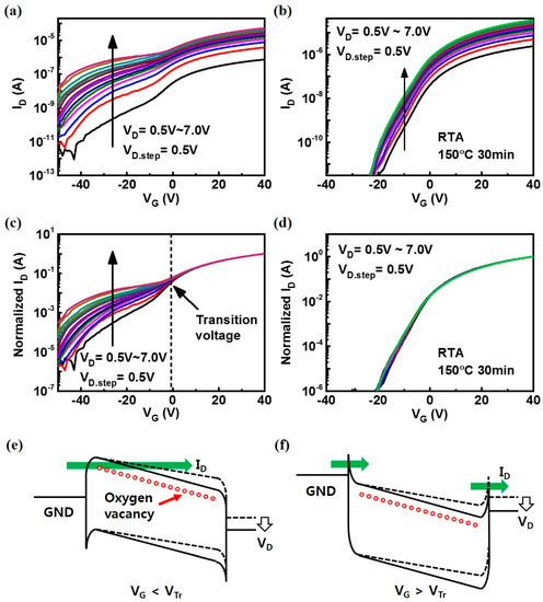
Figure 2.
ID–VG transfer curves measured at different VD (a) after low vacuum treatment (b) after RTA in oxygen ambient (150 °C for 30 min); (c,d) ID–VG transfer curves of (a) and (b), respectively, normalized with respect to ID at VG = 40 V; (e) Schematic band diagram for the case having VG below the transition voltage (VTr). Trap-assisted tunneling (TAT) current (green arrow) increased via an oxygen vacancy level near the conduction band of ZnO; (f) Schematic band diagram for the case having VG above VTr. The current (green arrow) flows through the Schottky barrier at source/channel and channel/drain without being affected by oxygen vacancies. The small red circles denote the expected energy level of oxygen vacancy.
The difference between the two groups becomes more evident with the normalized ID–VG curves as shown in Figure 2c,d. When the drain current curves measured at various VD are normalized with maximum Id value at the VG = 40 V, all I–V curves overlap each other. This result indicates that the relative difference in the drain current was due to the difference in the effective drain bias, i.e., series resistance component. In contrast, in a low field region, apparent drain current increase as a function of VD was observed in the devices stored in vacuum, which implies that the oxygen vacancies primarily contribute to the drain current increase at the low field region. These results also confirm that the oxygen vacancies generate shallow trap sites that contribute to the trap-assisted tunneling (TAT) from the source to the channel as schematically shown in Figure 2e [24,25]. At a high field region, these shallow traps do not directly contribute to the drain current because the carrier tunnel through the Schottky barrier becomes dominant as shown in Figure 2f. This model explains the gate bias dependence of oxygen vacancy induced hump and why they do not appear at the gate bias region above the specific bias marked in Figure 2c as a critical voltage, VTr. These results match those of the previous study on the impact of oxygen vacancy in ZnO particles [26,27].
Next, to estimate the effects of oxygen vacancies on the Schottky barrier at the channel/drain junction, constant voltage stress was performed as shown in Figure 3. In this process, negative drain bias stress was applied to the drain side (VD.stress = −2.5 V, VG.stress = 0 V) to probe the degradations in the channel/drain junction region. As the stress time increased, ID gradually changed from the red to the blue line as shown in Figure 3a. The ID drastically decreased at the VG region below VTr and this trend is reversed at the VG higher than VTr. This drastic decrease can be explained by the migrated positive charges at the drain side as illustrated in Figure 4a, which increases the TAT distance at the source side.
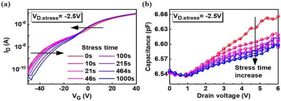
Figure 3.
(a) ID–VG transfer curves after negative bias stress. VD.stress = −2.5 V and stress time = 1000 s. Curves were shifted from the red to the blue line as indicated by the arrows; (b) gradual change in the source to drain capacitance as a function of drain voltage during the constant voltage stress. Capacitance was measured at VG = 0 V.
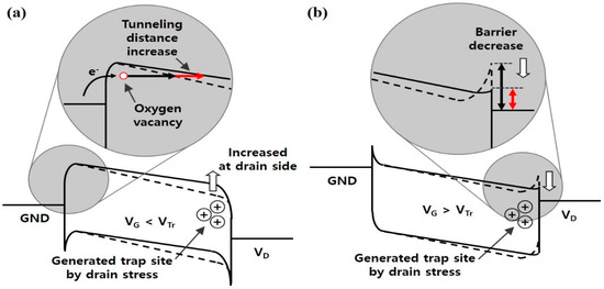
Figure 4.
(a) Energy band diagram when the VG is lower than the VTr with the enlarged region at the source/channel side. The tunneling distance of TAT (red arrow) increases due to the change in the potential barrier by positive charge traps near the channel/drain side; (b) Schottky barrier is lowered due to the charge traps when the VG is larger than the VTr near the channel/drain side after stress.
As shown in Figure 3b, the source to drain capacitance decreased from the red to the blue line as the stress time increased. At a higher VD, the decrease was more pronounced and the capacitance was decreased from 6.66 pF to 6.60 pF at VD = 6 V. Although the change in the junction capacitance is relatively small, it is apparent that the barrier profile of Schottky junction is indeed affected by the charge trapping as reported in the prior works on trap-induced Schottky barrier lowering [28,29] and illustrated in Figure 4b. Even though we cannot identify the band profile accurately from the capacitance measurement, the drain bias dependence and stress dependence indicates that the band profile shown in Figure 4 matches with the experimental results because the smaller capacitance means the smaller band bending by charge trapping.
Finally, the impact of constant voltage stress on the field effect mobility and on–current is investigated as shown in Figure 5. Interestingly, the field effect mobility increased after the stress, from 8.5 m2 V−1·s−1 to 8.9 m2 V−1·s−1, because the swing of ID–VG curve actually improved as shown in Figure 3a. This result is due to the suppression of subthreshold leakage current caused by the tunneling distance increase at the low gate bias region which can be explained with the band diagram shown in Figure 4a, which in turn improves the swing. The on-current values in the high field region were also enhanced after the stress by ~13% as shown in Figure 5b. This result can be explained by the band diagram shown in Figure 4b. After the negative drain bias stress, the traps accumulated in the drain side improve the channel conductivity due to the trap-induced Schottky barrier lowering effect.
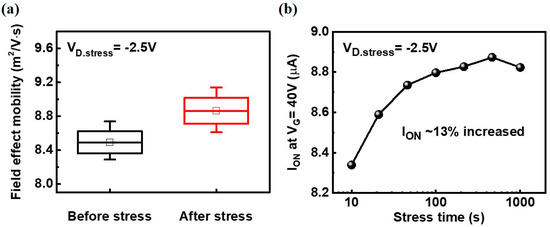
Figure 5.
Increase of the field-effect mobility (a) and on-current (b) after negative drain bias stress with reducing “hump” phenomenon. The field-effect mobility increased from ~8.5 cm2 V−1∙s−1 to ~8.9 cm2 V−1∙s−1 and on-current was increased by approximately 13% after negative drain bias stress by the trap-induced Schottky barrier lowering.
4. Conclusions
Various impacts of oxygen vacancies in ZnO channel were investigated. While we confirmed that the oxygen vacancies can be passivated with oxygen anneal, a new understanding of the device operating mechanism was accomplished through constant voltage stress on a drain. We found that the charge trapping in the drain side of the ZnO channel resulted in improved mobility, drain current and swing by modulating the Schottky barrier height and tunneling distance.
Author Contributions
S.C.K. measured and analyzed the electrical characteristics and S.Y.K. fabricated the devices. K.K., S.K.L., B.A. and H.J.H. supported the analysis of data and helped with the writing of the study. B.H.L. supported and guided the experiment and results. B.H.L. also conceived and advised during the publication of the study. All authors have read and agreed to the published version of the manuscript.
Funding
This study was partly supported by the Nano Materials Technology Development Program (2016M3A7B4909941), the Creative Materials Discovery Program (2015M3D1A1068062 and 2017M3D1A1040828) and the Global Frontier Hybrid Interface Materials (GFHIM) (2013M3A6B1078873) through the National Research Foundation (NRF) of Korea, funded by the Ministry of Science and ICT.
Conflicts of Interest
The authors declare no conflict of interest.
References
- Gandla, S.; Gollu, S.R.; Sharma, R.; Sarangi, V.; Gupta, D. Dual role of boron in improving electrical performance and device stability of low temperature solution processed ZnO thin film transistors. Appl. Phys. Lett. 2015, 107, 152102. [Google Scholar] [CrossRef]
- Cha, S.H.; Oh, M.S.; Lee, K.H.; Im, S.; Lee, B.H.; Sung, M.M. Electrically stable low voltage ZnO transistors with organic/inorganic nanohybrid dielectrics. Appl. Phys. Lett. 2008, 92, 023506. [Google Scholar] [CrossRef]
- Jun, J.H.; Park, B.; Cho, K.; Kim, S. Flexible TFTs based on solution-processed ZnO nanoparticles. Nanotechnology 2009, 20, 505201. [Google Scholar] [CrossRef] [PubMed]
- Masuda, S.; Kitamura, K.; Okumura, Y.; Miyatake, S.; Tabata, H.; Kawai, T. Transparent thin film transistors using ZnO as an active channel layer and their electrical properties. J. Appl. Phys. 2003, 93, 1624–1630. [Google Scholar] [CrossRef]
- Nishii, J.; Hossain, F.M.; Takagi, S.; Aita, T.; Saikusa, K.; Ohmaki, Y.; Ohkubo, I.; Kishimoto, S.; Ohtomo, A.; Fukumura, T.; et al. High Mobility Thin Film Transistors with Transparent ZnO Channels. Jpn. J. Appl. Phys. 2003, 42, L347. [Google Scholar] [CrossRef]
- Chiang, H.Q.; Wager, J.F.; Hoffman, R.L.; Jeong, J.; Keszler, D.A. High mobility transparent thin-film transistors with amorphous zinc tin oxide channel layer. Appl. Phys. Lett. 2004, 86, 013503. [Google Scholar] [CrossRef]
- Na, J.H.; Kitamura, M.; Arakawa, Y. High field-effect mobility amorphous InGaZnO transistors with aluminum electrodes. Appl. Phys. Lett. 2008, 93, 063501. [Google Scholar] [CrossRef]
- Kim, M.; Jeong, J.H.; Lee, H.J.; Ahn, T.K.; Shin, H.S.; Park, J.-S.; Jeong, J.K.; Mo, Y.-G.; Kim, H.D. High mobility bottom gate InGaZnO thin film transistors with SiOx etch stopper. Appl. Phys. Lett. 2007, 90, 212114. [Google Scholar] [CrossRef]
- Ryu, M.K.; Yang, S.; Park, S.-H.K.; Hwang, C.-S.; Jeong, J.K. High performance thin film transistor with cosputtered amorphous Zn–In–Sn–O channel: Combinatorial approach. Appl. Phys. Lett. 2009, 95, 072104. [Google Scholar] [CrossRef]
- Furuta, M.; Kamada, Y.; Kimura, M.; Hiramatsu, T.; Matsuda, T.; Furuta, H.; Li, C.; Fujita, S.; Hirao, T. Analysis of Hump Characteristics in Thin-Film Transistors With ZnO Channels Deposited by Sputtering at Various Oxygen Partial Pressures. IEEE Electron. Device Lett. 2010, 31, 1257–1259. [Google Scholar] [CrossRef]
- Chen, Y.-C.; Chang, T.-C.; Li, H.-W.; Chung, W.-F.; Chen, S.-C.; Wu, C.-P.; Chen, Y.-H.; Tai, Y.-H.; Tseng, T.-Y.; Yeh(Huang), F.-S. Characterization of environment-dependent hysteresis in indium gallium zinc oxide thin film transistors. Surf. Coat. Technol. 2013, 231, 531–534. [Google Scholar] [CrossRef]
- Huang, S.-Y.; Chang, T.-C.; Chen, M.-C.; Chen, S.-C.; Chen, T.-C.; Jian, F.-Y. Thermal Effect on the Gate-Drain Bias Stress for Amorphous InGaZnO Thin Film Transistors. Electrochem. Solid -State Lett. 2012, 15, H161–H163. [Google Scholar] [CrossRef]
- Janotti, A.; Van de Walle, C.G. Oxygen vacancies in ZnO. Appl. Phys. Lett. 2005, 87, 122102. [Google Scholar] [CrossRef]
- El-Atab, N.; Chowdhury, F.; Ulusoy, T.G.; Ghobadi, A.; Nazirzadeh, A.; Okyay, A.K.; Nayfeh, A. ~3-nm ZnO Nanoislands Deposition and Application in Charge Trapping Memory Grown by Single ALD Step. Sci. Rep. 2016, 6, 38712. [Google Scholar] [CrossRef] [PubMed]
- Um, J.G.; Mativenga, M.; Jang, J. Mechanism of positive bias stress-assisted recovery in amorphous-indium-gallium-zinc-oxide thin-film transistors from negative bias under illumination stress. Appl. Phys. Lett. 2013, 103, 033501. [Google Scholar] [CrossRef]
- Cho, Y.-J.; Kim, W.-S.; Lee, Y.-H.; Park, J.K.; Kim, G.T.; Kim, O. Effect of defect creation and migration on hump characteristics of a-InGaZnO thin film transistors under long-term drain bias stress with light illumination. Solid -State Electron. 2018, 144, 95–100. [Google Scholar] [CrossRef]
- Huang, X.; Wu, C.; Lu, H.; Ren, F.; Xu, Q.; Ou, H.; Zhang, R.; Zheng, Y. Electrical instability of amorphous indium-gallium-zinc oxide thin film transistors under monochromatic light illumination. Appl. Phys. Lett. 2012, 100, 243505. [Google Scholar] [CrossRef]
- Hong, S.; Park, S.P.; Kim, Y.; Kang, B.H.; Na, J.W.; Kim, H.J. Low-temperature fabrication of an HfO2 passivation layer for amorphous indium-gallium-zinc oxide thin film transistors using a solution process. Sci. Rep. 2017, 7, 16265. [Google Scholar] [CrossRef]
- Park, J.H.; Kim, Y.; Yoon, S.; Hong, S.; Kim, H.J. Simple Method to Enhance Positive Bias Stress Stability of In–Ga–Zn–O Thin-Film Transistors Using a Vertically Graded Oxygen-Vacancy Active Layer. ACS Appl. Mater. Interfaces 2014, 6, 21363–21368. [Google Scholar] [CrossRef]
- Hsieh, T.; Chang, T.; Chen, Y.; Liao, P.; Chen, T.; Tsai, M.; Chen, Y.; Chen, B.; Chu, A.; Chou, C.; et al. Hot-Carrier Effect on Amorphous In-Ga-Zn-O Thin-Film Transistors With a Via-Contact Structure. IEEE Electron. Device Lett. 2013, 34, 638–640. [Google Scholar] [CrossRef]
- Park, W.; Shaikh, S.F.; Min, J.-W.; Lee, S.K.; Lee, B.H.; Hussain, M.M. Contact resistance reduction of ZnO thin film transistors (TFTs) with saw-shaped electrode. Nanotechnology 2018, 29, 325202. [Google Scholar] [CrossRef] [PubMed]
- Kwon, S.; Bang, S.; Lee, S.; Jeon, S.; Jeong, W.; Kim, H.; Gong, S.C.; Chang, H.J.; Park, H.; Jeon, H. Characteristics of the ZnO thin film transistor by atomic layer deposition at various temperatures. Semicond. Sci. Technol. 2009, 24, 035015. [Google Scholar] [CrossRef]
- Levy, D.H.; Freeman, D.; Nelson, S.F.; Cowdery-Corvan, P.J.; Irving, L.M. Stable ZnO thin film transistors by fast open air atomic layer deposition. Appl. Phys. Lett. 2008, 92, 192101. [Google Scholar] [CrossRef]
- Paskaleva, A.; Lemberger, M.; Bauer, A.J.; Frey, L. Implication of oxygen vacancies on current conduction mechanisms in TiN/Zr1−xAlxO2/TiN metal-insulator-metal structures. J. Appl. Phys. 2011, 109, 076101. [Google Scholar] [CrossRef]
- Hara, T. Intentionally inserted oxygen depleted (Ba/sub 0.5/Sr/sub 0.5/)TiO/sub 3/ layers as a model of DC-electrical degradation. IEEE Trans. Device Mater. Reliab. 2004, 4, 670–675. [Google Scholar] [CrossRef]
- Zhang, M.; Averseng, F.; Haque, F.; Borghetti, P.; Krafft, J.-M.; Baptiste, B.; Costentin, G.; Stankic, S. Defect-related multicolour emissions in ZnO smoke: From violet, over green to yellow. Nanoscale 2019, 11, 5102–5115. [Google Scholar] [CrossRef]
- Drouilly, C.; Krafft, J.-M.; Averseng, F.; Casale, S.; Bazer-Bachi, D.; Chizallet, C.; Lecocq, V.; Vezin, H.; Lauron-Pernot, H.; Costentin, G. ZnO Oxygen Vacancies Formation and Filling Followed by in Situ Photoluminescence and in Situ EPR. J. Phys. Chem. C 2012, 116, 21297–21307. [Google Scholar] [CrossRef]
- Omar, S.U.; Sudarshan, T.S.; Rana, T.A.; Song, H.; Chandrashekhar, M.V.S. Interface Trap-Induced Nonideality in As-Deposited Ni/4H-SiC Schottky Barrier Diode. IEEE Trans. Electron. Devices 2015, 62, 615–621. [Google Scholar] [CrossRef]
- Wager, J.F. Transparent electronics: Schottky barrier and heterojunction considerations. Thin Solid Films 2008, 516, 1755–1764. [Google Scholar] [CrossRef]
© 2020 by the authors. Licensee MDPI, Basel, Switzerland. This article is an open access article distributed under the terms and conditions of the Creative Commons Attribution (CC BY) license (http://creativecommons.org/licenses/by/4.0/).