Performance Enhancement of Ultra-Thin Nanowire Array Solar Cells by Bottom Reflectivity Engineering


Abstract
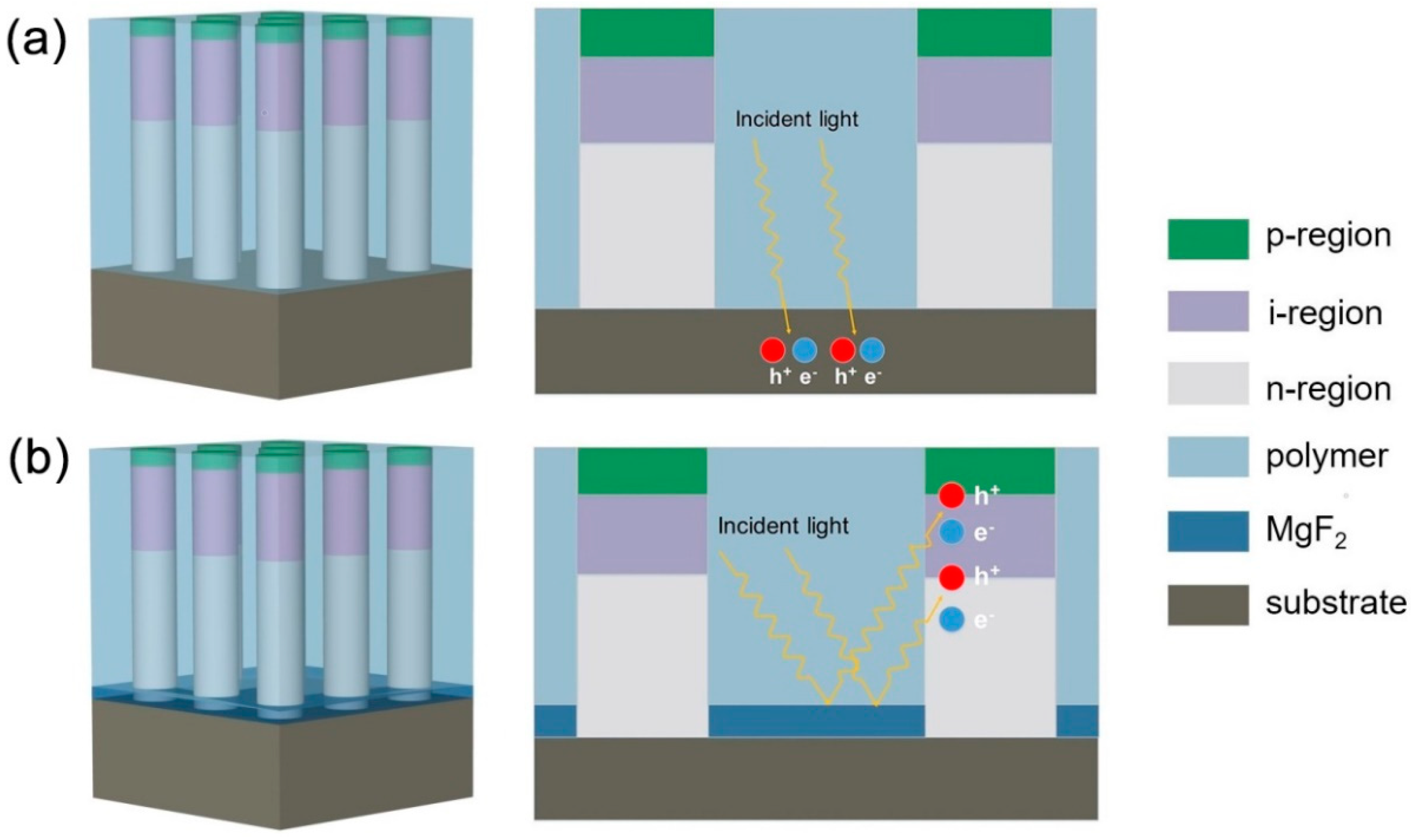
:1. Introduction
2. Methods
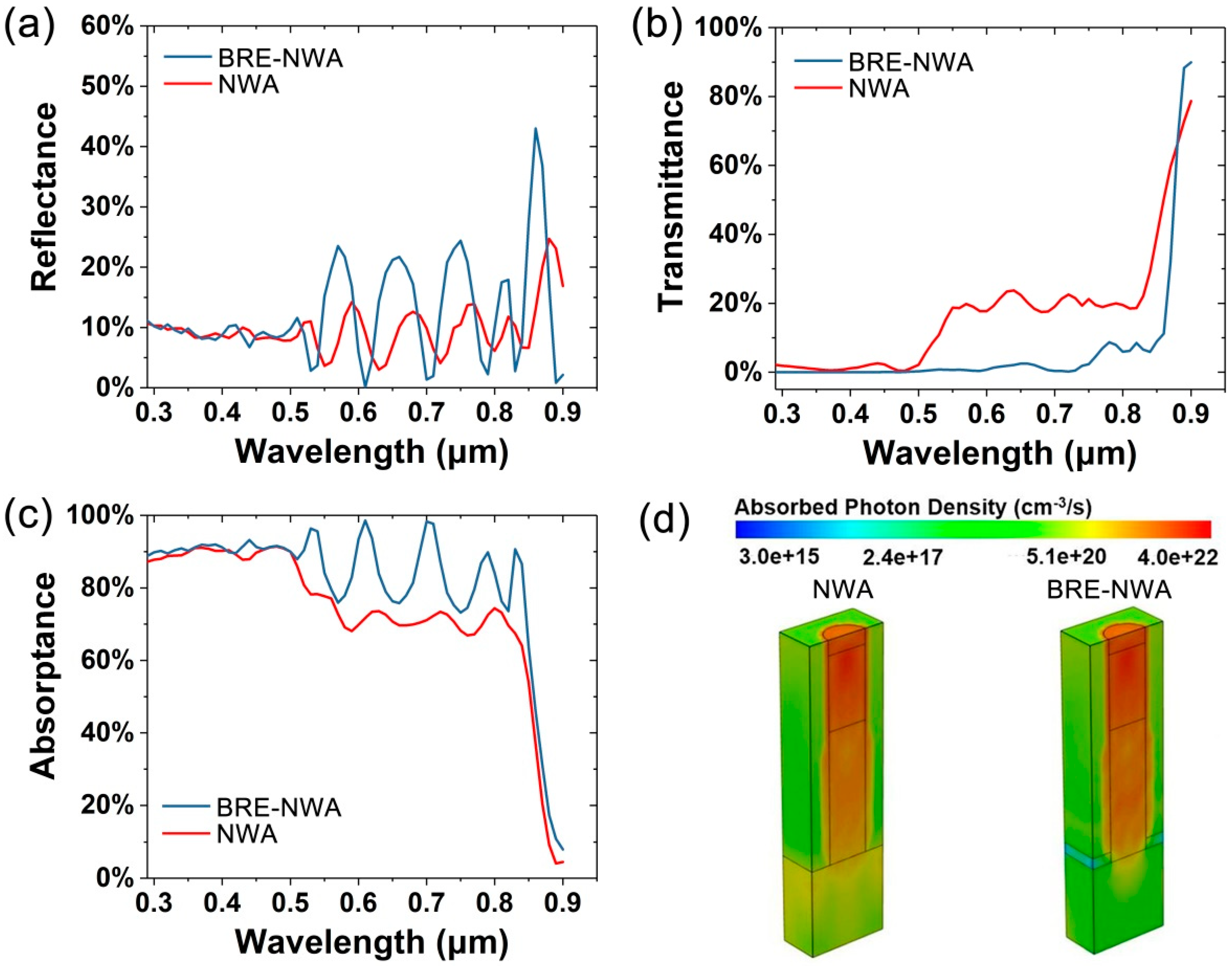
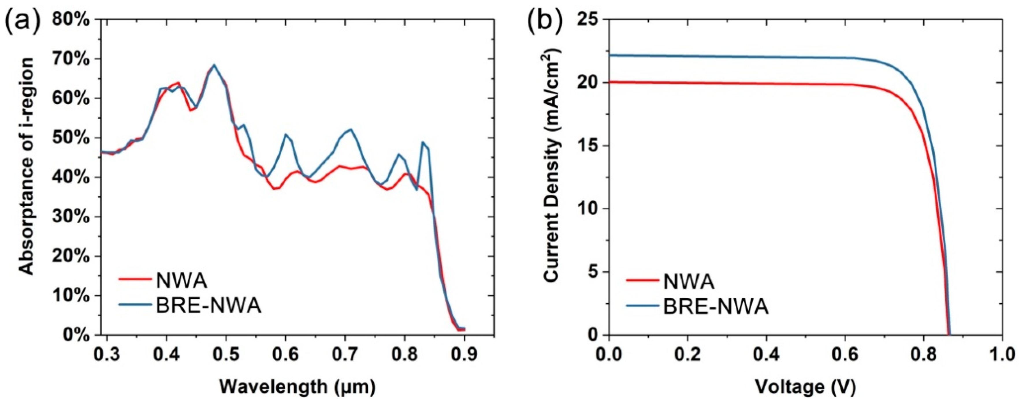
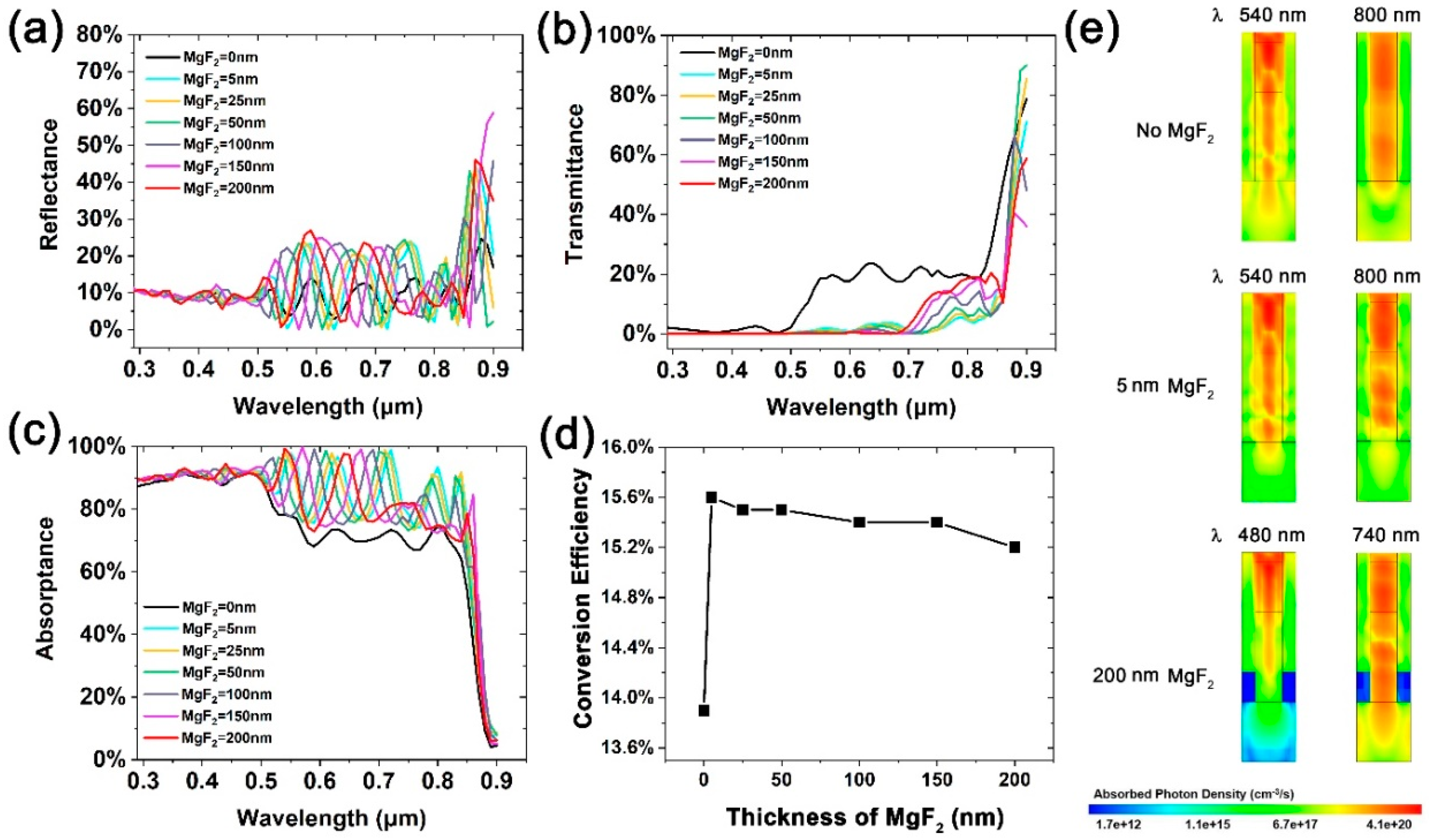
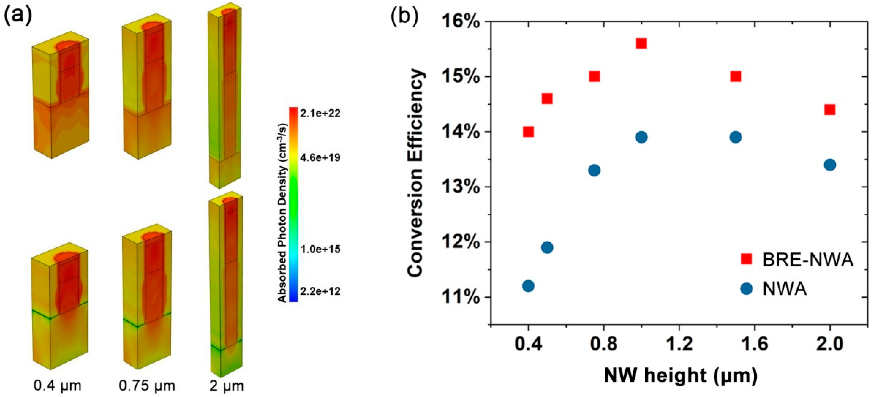
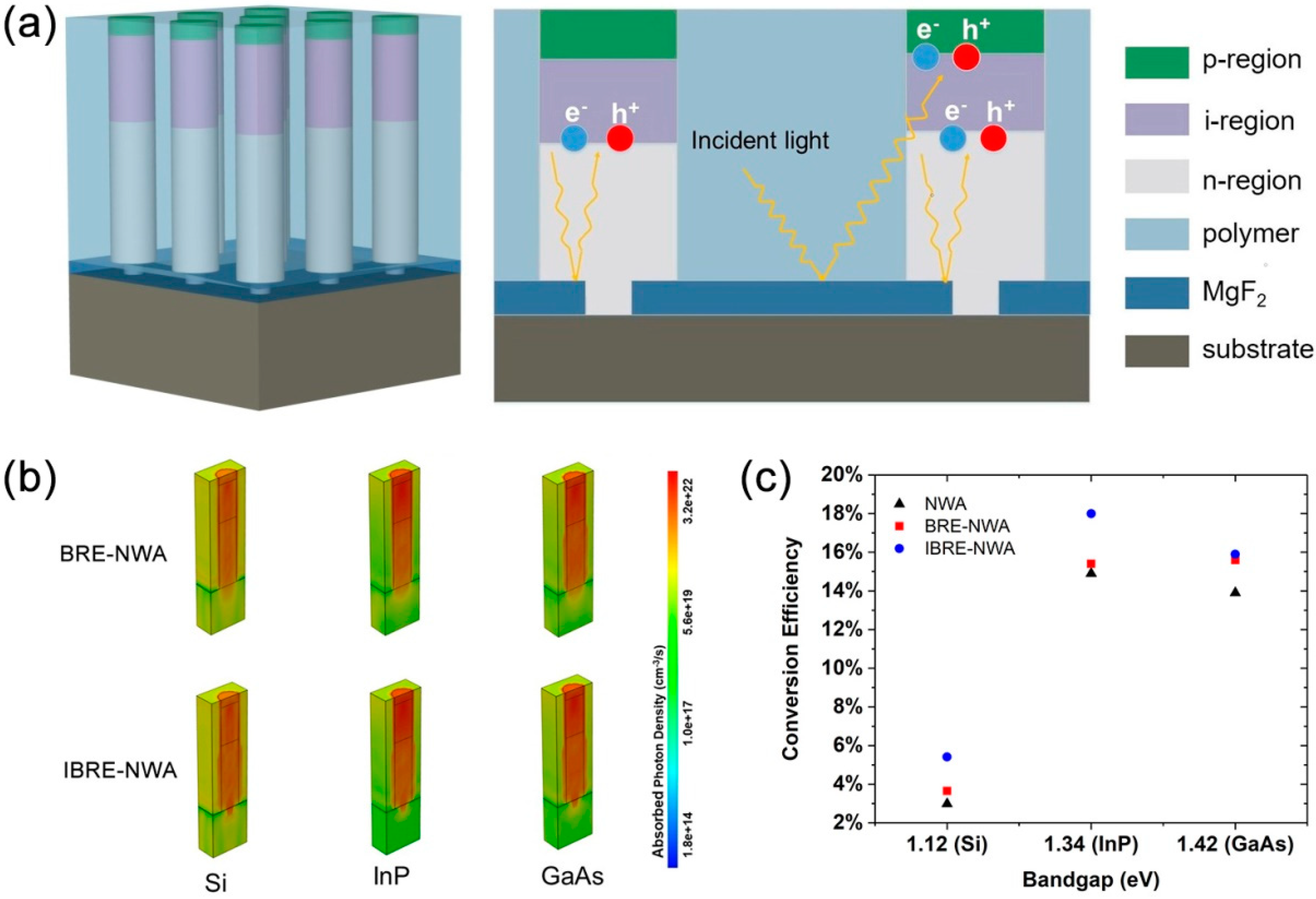
3. Results and Discussion
4. Conclusions
Author Contributions
Funding
Acknowledgments
Conflicts of Interest
References
- Yuan, J.; Zhang, Y.; Zhou, L.; Zhang, G.; Yip, H.-L.; Lau, T.-K.; Lu, X.; Zhu, C.; Peng, H.; Johnson, P.A.; et al. Single-junction organic solar cell with over 15% efficiency using fused-ring acceptor with electron-deficient core. Joule 2019, 3, 1140–1151. [Google Scholar] [CrossRef]
- Green, M.A.; Ho-Baillie, A.; Snaith, H.J. The emergence of perovskite solar cells. Nat. Photonics 2014, 8, 506–514. [Google Scholar] [CrossRef]
- Chuang, I.; Lee, B.; He, J.; Chang, R.P.H.; Kanatzidis, M.G. All-solid-state dye-sensitized solar cells with high efficiency. Nature 2012, 485, 486–489. [Google Scholar] [CrossRef] [PubMed]
- Garnett, E.C.; Brongersma, M.L.; Cui, Y.; McGehee, M.D. Nanowire solar cells. Annu. Rev. Mater. Res. 2011, 41, 269–295. [Google Scholar] [CrossRef] [Green Version]
- Meng, L.; Zhang, Y.; Wan, X.; Li, C.; Zhang, X.; Wang, Y.; Ke, X.; Xiao, Z.; Ding, L.; Xia, R.; et al. Organic and solution-processed tandem solar cells with 17.3% efficiency. Science 2018, 14, 1094–1098. [Google Scholar] [CrossRef] [Green Version]
- Wallentin, J.; Anttu, N.; Asoli, D.; Huffman, M.; Åberg, I.; Magnusson, M.H.; Siefer, G.; Fuss-Kailuweit, P.; Dimroth, F.; Witzigmann, B.; et al. InP nanowire array solar cells achieving 13.8% efficiency by exceeding the ray optics limit. Science 2013, 339, 1057–1060. [Google Scholar] [CrossRef] [Green Version]
- Guo, H.; Wen, L.; Li, X.; Zhao, Z.; Wang, Y. Analysis of optical absorption in GaAs nanowire arrays. Nanoscale Res. Lett. 2011, 6, 617. [Google Scholar] [CrossRef] [Green Version]
- Xie, W.Q.; Oh, J.I.; Shen, W.Z. Realization of effective light trapping and omnidirectional antireflection in smooth surface silicon nanowire arrays. Nanotechnology 2011, 22, 065704. [Google Scholar] [CrossRef]
- Krogstrup, P.; Jørgensen, H.I.; Heiss, M.; Demichel, O.; Holm, J.V.; Aagesen, M.; Nygard, J.; Morral, A.F. Single-nanowire solar cells beyond the Shockley–Queisser limit. Nat. Photonics 2013, 7, 306–310. [Google Scholar] [CrossRef] [Green Version]
- LaPierre, R.R. Theoretical conversion efficiency of a two-junction III–V nanowire on Si solar cell. J. Appl. Phys. 2011, 110, 014310. [Google Scholar] [CrossRef]
- Wen, L.; Li, X.; Zhao, Z.; Bu, S.; Zeng, X.; Huang, J.; Wang, Y. Theoretical consideration of III–V nanowire/Si triple-junction solar cells. Nanotechnology 2012, 23, 505202. [Google Scholar] [CrossRef] [PubMed]
- Yao, M.; Cong, S.; Arab, S.; Huang, N.; Povinelli, M.L.; Cronin, S.B.; Dapkus, P.D.; Zhou, C. Tandem solar cells using GaAs nanowires on Si: Design, fabrication, and observation of voltage addition. Nano Lett. 2015, 15, 7217–7224. [Google Scholar] [CrossRef] [PubMed]
- Borgström, M.T.; Magnusson, M.H.; Dimroth, F.; Siefer, G.; Höhn, O.; Riel, H.; Schmid, H.; Wirths, S.; Björk, M.; Åberg, I.; et al. Towards nanowire tandem junction solar vells on silicon. IEEE J. Photovolt. 2018, 8, 733–740. [Google Scholar]
- Åberg, I.; Vescovi, G.; Asoli, D.; Naseem, U.; Gilboy, J.P.; Sundvall, C.; Dahlgren, A.K.; Svensson, E.; Anttu, N.; Björk, M.T.; et al. A GaAs nanowire array solar cell with 15.3% efficiency at 1 sun. IEEE J. Photovolt. 2015, 6, 185–190. [Google Scholar] [CrossRef]
- Garnett, E.C.; Yang, P. Silicon nanowire radial p-n junction solar cells. J. Am. Chem. Soc. 2008, 130, 9224–9225. [Google Scholar] [CrossRef]
- Tang, Y.B.; Chen, Z.H.; Song, H.S.; Lee, C.S.; Cong, H.T.; Cheng, H.M.; Zhang, W.J.; Bello, I.; Lee, S.T. Vertically aligned p-type single-crystalline GaN nanorod arrays on n-type Si for heterojunction photovoltaic cells. Nano Lett. 2008, 8, 4191–4195. [Google Scholar] [CrossRef]
- Shin, J.C.; Lee, A.; Mohseni, P.K.; Kim, D.Y.; Yu, L.; Kim, J.H.; Kim, H.J.; Choi, W.J.; Wasserman, D.; Choi, K.J.; et al. Wafer-scale production of uniform InAsyP1–y nanowire array on silicon for heterogeneous integration. ACS Nano 2013, 7, 5463–5471. [Google Scholar] [CrossRef]
- Mallorquí, A.D.; Alarcón-Lladó, E.; Russo-Averchi, E.; Tütüncüoglu, G.; Matteini, F.; Rüffer, D.; Morral, A.F. Characterization and analysis of InAs/p-Si heterojunction nanowire-based solar cell. J. Phys. D Appl. Phys. 2014, 47, 394017. [Google Scholar] [CrossRef] [Green Version]
- Yan, X.; Gong, L.; Ai, L.; Wei, W.; Zhang, X.; Ren, X. Enhanced photovoltaic performance of nanowire array solar cells with multiple diameters. Opt. Express 2018, 26, A974–A983. [Google Scholar] [CrossRef]
- Li, J.; Yu, H.; Wong, S.M.; Li, X.; Zhang, G.; Lo, P.G.; Kwong, D.-L. Design guidelines of periodic Si nanowire arrays for solar cell application. Appl. Phys. Lett. 2009, 95, 243113. [Google Scholar] [CrossRef]
- Wang, B.; Leu, P.W. Enhanced absorption in silicon nanocone arrays for photovoltaics. Nanotechnology 2012, 23, 194003. [Google Scholar] [CrossRef] [PubMed]
- Zhang, J.; Ai, L.; Yan, X.; Wu, Y.; Wei, W.; Zhang, M.; Zhang, X. Photovoltaic performance of pin junction nanocone array solar cells with enhanced effective optical absorption. Nanoscale Res. Lett. 2018, 13, 306. [Google Scholar] [CrossRef] [PubMed]
- Wu, Y.; Yan, X.; Zhang, X.; Ren, X. Enhanced photovoltaic performance of an inclined nanowire array solar cell. Opt. Express 2015, 23, A1603–A1612. [Google Scholar] [CrossRef] [PubMed]
- Wu, Y.; Yan, X.; Zhang, X.; Ren, X. Photovoltaic performance of a nanowire/quantum dot hybrid nanostructure array solar cell. Nanoscale Res. Lett. 2018, 13, 62. [Google Scholar] [CrossRef] [Green Version]
- Li, Y.; Yan, X.; Wu, Y.; Zhang, X.; Ren, X. Plasmon-enhanced light absorption in GaAs nanowire array solar cells. Nanoscale Res. Lett. 2015, 10, 436. [Google Scholar] [CrossRef] [Green Version]
- Dadabayev, R.; Malka, D. A visible light RGB wavelength demultiplexer based on polycarbonate multicore polymer optical fiber. Opt. Laser Technol. 2019, 116, 239–245. [Google Scholar] [CrossRef]
- Mariani, G.; Wong, P.-S.; Katzenmeyer, A.M.; Léonard, F.; Shapiro, J.; Huffaker, D.L. Patterned radial GaAs nanopillar solar cells. Nano Lett. 2011, 11, 2490–2494. [Google Scholar] [CrossRef]
- Yao, M.; Huang, N.; Cong, S.; Chi, C.-Y.; Seyedi, M.A.; Lin, Y.-T.; Cao, Y.; Povinelli, M.L.P.; Dapkus, P.D.; Zhou, C. GaAs nanowire array solar cells with axial p-i-n junctions. Nano Lett. 2014, 14, 3293–3303. [Google Scholar] [CrossRef]
- Pinhas, H.; Malka, D.; Danan, Y.; Sinvani, M.; Zalevsky, Z. Design of fiber-integrated tunable thermo-optic C-band filter based on coated silicon. J. Eur. Opt. Soc. Rapid 2017, 13, 32. [Google Scholar] [CrossRef] [Green Version]
- Malka, D.; Berke, B.A.; Tischler, Y.; Zalevsky, Z. Improving Raman spectra of pure silicon using super-resolved method. J. Opt. 2019, 21, 075801. [Google Scholar] [CrossRef]
- Tomioka, K.; Kobayashi, Y.; Motohisa, J.; Hara, S.; Fukui, T. Selective-area growth of vertically aligned GaAs and GaAs/AlGaAs core–shell nanowires on Si(111) substrate. Nanotechnology 2009, 20, 145302. [Google Scholar] [CrossRef] [PubMed] [Green Version]
- Goto, H.; Nosaki, K.; Tomioka, K.; Hara, S.; Hiruma, K.; Motohisa, J.; Fukui, T. Growth of core–shell InP nanowires for photovoltaic application by selective-area metal organic vapor phase epitaxy. Appl. Phys. Express 2009, 2, 035004. [Google Scholar] [CrossRef]
- Nakai, E.; Yoshimura, M.; Tomioka, K.; Fukui, T. GaAs/InGaP core–multishell nanowire-array-based solar cells. Jpn. J. Appl. Phys. 2013, 52, 055002. [Google Scholar] [CrossRef] [Green Version]
- Alekseev, P.A.; Dunaevskiy, M.S.; Ulin, V.P.; Lvova, T.V.; Filatov, D.O.; Nezhdanov, A.V.; Mashin, A.I.; Berkovits, V.L. Nitride surface passivation of GaAs nanowires: Impact on surface state density. Nano Lett. 2015, 15, 63–68. [Google Scholar] [CrossRef] [PubMed]
- Sheldon, M.T.; Eisler, C.N.; Atwater, H.A. GaAs Passivation with Trioctylphosphine sulfide for enhanced solar cell efficiency and durability. Adv. Energy Mater. 2012, 2, 339–344. [Google Scholar] [CrossRef]
- Tajik, N.; Peng, Z.; Kuyanov, P.; LaPierre, R.R. Sulfur passivation and contact methods for GaAs nanowire solar cells. Nanotechnology 2011, 22, 225402. [Google Scholar] [CrossRef] [PubMed]
- Levinshtein, M.; Rumyantsev, S.; Shur, M. Handbook Series on Semiconductor Parameters: Ternary and Quaternary III–V Compounds; World Scientific: Singapore, 1999. [Google Scholar]
- Beadie, G.; Brindza, M.; Flynn, R.A.; Rosenberg, A.; Shirk, J.S. Refractive index measurements of poly(methyl methacrylate) (PMMA) from 0.4–1.6 μm. Appl. Opt. 2015, 54, F139–F143. [Google Scholar] [CrossRef]
- Dodge, M.J. Refractive properties of magnesium fluoride. Appl. Opt. 1984, 23, 1980–1985. [Google Scholar] [CrossRef]
- Hu, Y.; LaPierre, R.R.; Li, M.; Chen, K.; He, J.-J. Optical characteristics of GaAs nanowire solar cells. J. Appl. Phys. 2012, 112, 104311. [Google Scholar] [CrossRef]
- Willis, S.M.; Dimmock, J.A.R.; Tutu, F.; Liu, H.Y.; Peinado, M.G.; Assender, H.E.; Watt, A.A.R.; Sellers, I.R. Defect mediated extraction in InAs/GaAs quantum dot solar cells. Sol. Energy Mater. Sol. Cells 2012, 102, 142–147. [Google Scholar] [CrossRef]
- Gorji, N.E. A theoretical approach on the strain-induced dislocation effects in the quantum dot solar cells. Sol. Energy 2012, 86, 935–940. [Google Scholar] [CrossRef]
- Cui, Y.; Wang, J.; Plissard, S.R.; Cavalli, A.; Vu, T.T.T.; Veldhoven, P.J.; Gao, L.; Trainor, M.; Verheijen, M.A.; Haverkort, J.E.M.; et al. Efficiency enhancement of InP nanowire solar cells by surface cleaning. Nano Lett. 2013, 13, 4113–4117. [Google Scholar] [CrossRef] [PubMed]
- Wang, X.; Pey, K.L.; Yip, C.H.; Fitzgerald, E.A.; Antoniadis, D.A. Vertically arrayed Si nanowire/nanorod-based core-shell p-n junction solar cells. J. Appl. Phys. 2010, 108, 124303. [Google Scholar] [CrossRef]

| Material | Fill Factor (%) | Efficiency (%) | Reference | ||
|---|---|---|---|---|---|
| GaAs | 0.868 | 22.7 | 80.5 | 15.9 | This work |
| GaAs | 0.906 | 21.3 | 79.2 | 15.3 | [14] |
| GaAs | 0.565 | 21.08 | 63.65 | 7.58 | [28] |
| InP | 0.835 | 24.9 | 86.3 | 18 | This work |
| InP | 0.779 | 24.6 | 72.4 | 13.8 | [6] |
| InP | 0.73 | 21 | 73 | 11.1 | [43] |
| Si | 0.559 | 11.8 | 82.3 | 5.4 | This work |
| Si | 0.45 | 6.34 | 53 | 1.47 | [44] |
| Si | 0.29 | 4.28 | 33 | 0.46 | [15] |
© 2020 by the authors. Licensee MDPI, Basel, Switzerland. This article is an open access article distributed under the terms and conditions of the Creative Commons Attribution (CC BY) license (http://creativecommons.org/licenses/by/4.0/).
Share and Cite
Yan, X.; Liu, H.; Sibirev, N.; Zhang, X.; Ren, X. Performance Enhancement of Ultra-Thin Nanowire Array Solar Cells by Bottom Reflectivity Engineering. Nanomaterials 2020, 10, 184. https://doi.org/10.3390/nano10020184
Yan X, Liu H, Sibirev N, Zhang X, Ren X. Performance Enhancement of Ultra-Thin Nanowire Array Solar Cells by Bottom Reflectivity Engineering. Nanomaterials. 2020; 10(2):184. https://doi.org/10.3390/nano10020184
Chicago/Turabian StyleYan, Xin, Haoran Liu, Nickolay Sibirev, Xia Zhang, and Xiaomin Ren. 2020. "Performance Enhancement of Ultra-Thin Nanowire Array Solar Cells by Bottom Reflectivity Engineering" Nanomaterials 10, no. 2: 184. https://doi.org/10.3390/nano10020184
APA StyleYan, X., Liu, H., Sibirev, N., Zhang, X., & Ren, X. (2020). Performance Enhancement of Ultra-Thin Nanowire Array Solar Cells by Bottom Reflectivity Engineering. Nanomaterials, 10(2), 184. https://doi.org/10.3390/nano10020184