Resist-Free Directed Self-Assembly Chemo-Epitaxy Approach for Line/Space Patterning


Abstract
1. Introduction
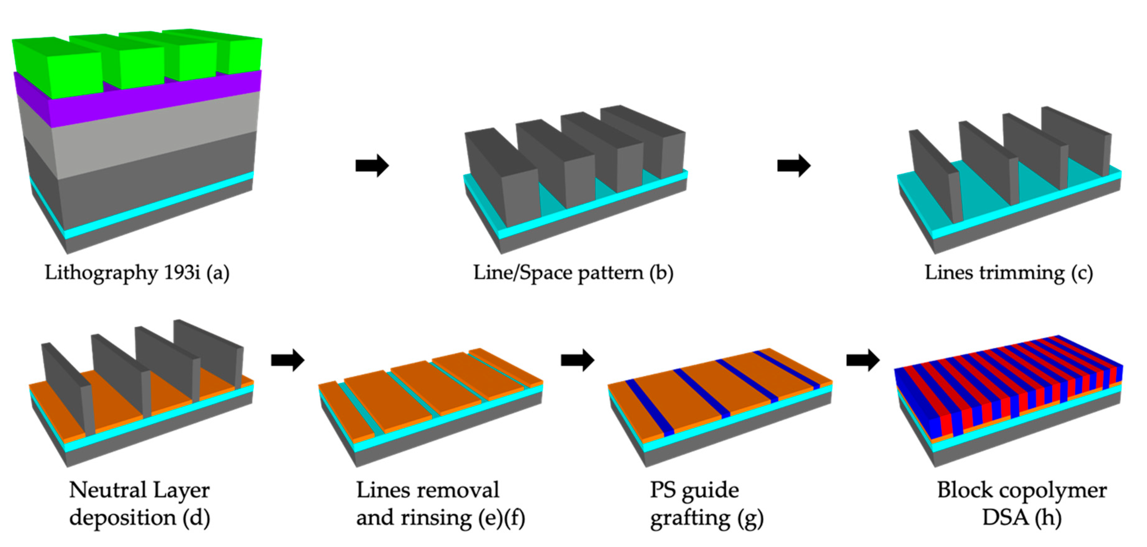
2. Experimental
2.1. Materials
- -
- Cross-linked PS-r-PMMA (NLa) layer
- -
- Functionalized PS-r-PMMA (NLb) with high molar mass
- -
- Functionalized PS-r-PMMA (NLc) with low molar mass
- -
- Functionalized PS-r-PMMA (NLd) with low molar mass (comparable to NLc) and different fractions of PS with respect to NLc.
2.2. Characterization
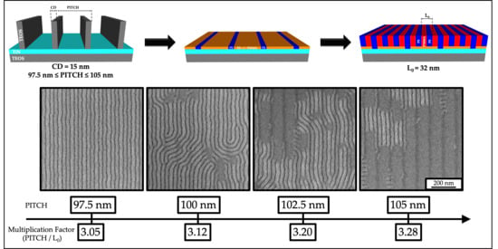
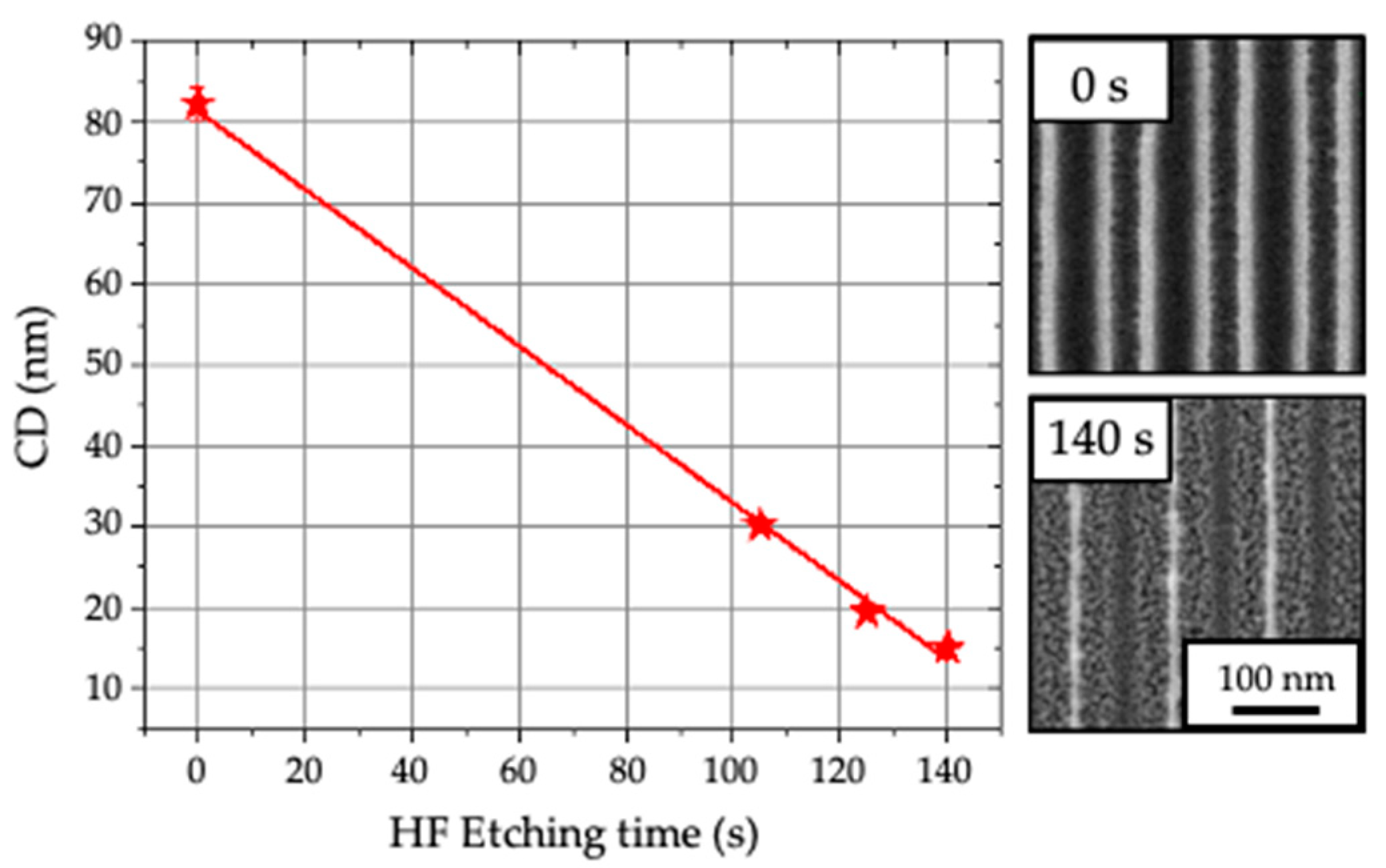
3. Results
4. Discussions
5. Conclusions
6. Patents
Supplementary Materials
Author Contributions
Funding
Acknowledgments
Conflicts of Interest
References
- Rahman, A.; Ashraf, A.; Xin, H.; Tong, X.; Sutter, P.; Eisaman, M.D.; Black, C.T. Sub-50-nm self-assembled nanotextures for enhanced broadband antireflection in silicon solar cells. Nat. Commun. 2015, 6, 5963. [Google Scholar] [CrossRef] [PubMed]
- Stefik, M.; Guldin, S.; Vignolini, S.; Wiesner, U.; Steiner, U. Block copolymer self-assembly for nanophotonics. Chem. Soc. Rev. 2015, 44, 5076–5091. [Google Scholar] [CrossRef]
- Yi, H.; Bao, X.Y.; Tiberio, R.; Philip Wong, H.S. A General Design Strategy for Block Copolymer Directed Self-Assembly Patterning of Integrated Circuits Contact Holes using an Alphabet Approach. Nano Lett. 2015, 15, 805–812. [Google Scholar] [CrossRef] [PubMed]
- Yu, H.; Qiu, X.; Moreno, N.; Ma, Z.; Calo, V.M.; Nunes, S.P.; Peinemann, K.V. Self-Assembled Asymmetric Block Copolymer Membranes: Bridging the Gap from Ultra- to Nanofiltration. Angew. Chem. Int. Ed. 2015, 54, 13937–13941. [Google Scholar] [CrossRef]
- Bates, F.S. Polymer-Polymer Phase Behavior. Science 1991, 251, 898–905. [Google Scholar] [CrossRef] [PubMed]
- Lo, T.-Y.; Krishnan, M.R.; Lu, K.-Y.; Ho, R.-M. Silicon-containing block copolymers for lithographic applications. Prog. Polym. Sci. 2017. [Google Scholar] [CrossRef]
- Giammaria, T.J.; Ferrarese Lupi, F.; Seguini, G.; Perego, M.; Vita, F.; Francescangeli, O.; Wenning, B.; Ober, C.K.; Sparnacci, K.; Antonioli, D.; et al. Micrometer-Scale Ordering of Silicon-Containing Block Copolymer Thin Films via High-Temperature Thermal Treatments. ACS Appl. Mater. Interfaces 2016, 8, 9897–9908. [Google Scholar] [CrossRef]
- Giammaria, T.J.; Laus, M.; Perego, M. Technological strategies for self-assembly of ps-b-pdms in cylindrical sub-10 nm nanostructures for lithographic applications. Adv. Phys. X 2018, 3, 391–411. [Google Scholar] [CrossRef]
- Ji, S.; Wan, L.; Liu, C.-C.; Nealey, P.F. Directed self-assembly of block copolymers on chemical patterns: A platform for nanofabrication. Prog. Polym. Sci. 2016, 54–55, 76–127. [Google Scholar] [CrossRef]
- Tiron, R.; Chevalier, X.; Couderc, C.; Pradelles, J.; Bustos, J.; Pain, L.; Navarro, C.; Magnet, S.; Fleury, G.; Hadziioannou, G. Optimization of block copolymer self-assembly through graphoepitaxy: A defectivity study. J. Vac. Sci. Technol. B 2011, 29, 06F206. [Google Scholar] [CrossRef]
- Cheng, J.; Doerk, G.S.; Rettner, C.T.; Singh, G.; Tjio, M.; Truong, H.; Arellano, N.; Balakrishnan, S.; Brink, M.; Tsai, H.; et al. Customization and design of directed self-assembly using hybrid prepatterns. Proc. SPIE 9423 Altern. Lithogr. Technol. VII 2015, 942307. [Google Scholar] [CrossRef]
- Cheng, J.Y.; Sanders, D.P.; Truong, H.D.; Harrer, S.; Friz, A.; Holmes, S.; Colburn, M.; Hinsberg, W.D. Simple and Versatile Methods To Integrate Directed Self-Assembly with Optical Lithography Using a Polarity-Switched Photoresist. ACS Nano 2010, 4, 4815–4823. [Google Scholar] [CrossRef] [PubMed]
- Wan, L.; Ruiz, R.; Gao, H.; Albrecht, T.R. Self-Registered Self-Assembly of Block Copolymers. ACS Nano 2017, 11, 7666–7673. [Google Scholar] [CrossRef] [PubMed]
- Cushen, J.; Wan, L.; Blachut, G.; Maher, M.J.; Albrecht, T.R.; Ellison, C.J.; Willson, C.G.; Ruiz, R. Double-Patterned Sidewall Directed Self-Assembly and Pattern Transfer of Sub-10 nm PTMSS-b-PMOST. ACS Appl. Mater. Interfaces 2015, 7, 13476–13483. [Google Scholar] [CrossRef] [PubMed]
- Liu, C.-C.; Ramírez-Hernández, A.; Han, E.; Craig, G.S.W.; Tada, Y.; Yoshida, H.; Kang, H.; Ji, S.; Gopalan, P.; de Pablo, J.J.; et al. Chemical Patterns for Directed Self-Assembly of Lamellae-Forming Block Copolymers with Density Multiplication of Features. Macromolecules 2013, 46, 1415–1424. [Google Scholar] [CrossRef]
- Kim, J.; Wan, J.; Miyazaki, S.; Yin, J.; Cao, Y.; Her, Y.J.; Wu, H.; Shan, J.; Kurosawa, K.; Lin, G. The SMARTTM process for directed block co-polymer self-assembly. J. Photopolym. Sci. Technol. 2013, 26, 573–579. [Google Scholar] [CrossRef][Green Version]
- Seino, Y.; Kasahara, Y.; Sato, H.; Kobayashi, K.; Miyagi, K.; Minegishi, S.; Kodera, K.; Kanai, H.; Tobana, T.; Kihara, N.; et al. A novel simple sub-15nm line-and-space patterning process flow using directed self-assembly technology. Microelectron. Eng. 2015, 134, 27–32. [Google Scholar] [CrossRef]
- Paquet, A.; Le Pennec, A.; Gharbi, A.; Giammaria, T.J.; Rademaker, G.; Pourteau, M.-L.; Mariolle, D.; Navarro, C.; Nicolet, C.; Chevalier, X.; et al. Spacer patterning lithography as a new process to induce block copolymer alignment by chemo-epitaxy. Proc. SPIE 10958 Nov. Patterning Technol. Semicond. MEMS/NEMS MOEMS 2019, 109580M. [Google Scholar] [CrossRef]
- Murphy, J.N.; Harris, K.D.; Buriak, J.M. Automated Defect and Correlation Length Analysis of Block Copolymer Thin Film Nanopatterns. PLoS ONE 2015, 10, e0133088. [Google Scholar] [CrossRef]
- Spierings, G.A.C.M. Wet chemical etching of silicate glasses in hydrofluoric acid based solutions. J. Mater. Sci. 1993, 28, 6261–6273. [Google Scholar] [CrossRef]
- Kim, H.W.; Lee, J.Y.; Shin, J.; Woo, S.G.; Cho, H.K.; Moon, J.T. Experimental investigation of the impact of LWR on sub-100-nm device performance. IEEE Trans. Electron. Devices 2004, 51, 1984–1988. [Google Scholar] [CrossRef]
- Qiang, Z.; Zhang, L.; Stein, G.E.; Cavicchi, K.A.; Vogt, B.D. Unidirectional Alignment of Block Copolymer Films Induced by Expansion of a Permeable Elastomer during Solvent Vapor Annealing. Macromolecules 2014, 47, 1109–1116. [Google Scholar] [CrossRef]
- Jung, Y.S.; Ross, C.A. Orientation-controlled self-assembled nanolithography using a polystyrene—Polydimethylsiloxane block copolymer. Nano Lett. 2007, 7, 2046–2050. [Google Scholar] [CrossRef] [PubMed]
- Sparnacci, K.; Chiarcos, R.; Gianotti, V.; Laus, M.; Giammaria, T.J.; Perego, M.; Munaò, G.; Milano, G.; De Nicola, A.; Haese, M.; et al. Effect of Trapped Solvent on the Interface between PS-b-PMMA Thin Films and P(S-r-MMA) Brush Layers. ACS Appl. Mater. Interfaces 2020, 12, 7777–7787. [Google Scholar] [CrossRef] [PubMed]
- Lee, H.; Jo, S.; Hirata, T.; Yamada, N.L.; Tanaka, K.; Kim, E.; Yeol, D. Interpenetration of chemically identical polymer onto grafted substrates. Polymer 2015, 74, 70–75. [Google Scholar] [CrossRef]
- Gay, C. Wetting of a Polymer Brush by a Chemically Identical Polymer Melt. Macromolecules 1997, 30, 5939–5943. [Google Scholar] [CrossRef]
- The International Technology Roadmap for Semiconductors 2.0: Lithography, 2015. Available online: http://www.itrs2.net/itrs-reports.html (accessed on 1 November 2020).
- International Roadmap for Devices and Systems 2017 Edition: Lithography, 2017. Available online: https://irds.ieee.org/editions/2017 (accessed on 1 November 2020).
- Asenov, A.; Kaya, S.; Brown, A.R. Intrinsic parameter fluctuations in decananometer MOSFETs introduced by gate line edge roughness. IEEE Trans. Electron. Devices 2003, 50, 1254–1260. [Google Scholar] [CrossRef]
- Steinhögl, W.; Schindler, G.; Steinlesberger, G.; Traving, M.; Engelhardt, M. Impact of line edge roughness on the resistivity of nanometer-scale interconnects. Microelectron. Eng. 2004, 76, 126–130. [Google Scholar] [CrossRef]
- Stucchi, M.; Bamal, M.; Maex, K. Impact of line-edge roughness on resistance and capacitance of scaled interconnects. Microelectron. Eng. 2007, 84, 2733–2737. [Google Scholar] [CrossRef]
- Seidel, R.; Williamson, L.; Her, Y.; Kim, J.; Lin, G.; Nealey, P.; Gronheid, R. The role of guide stripe chemistry in block copolymer directed self-assembly. Adv. Patterning Mater. Process. XXXII 2015, 9425, 94250W. [Google Scholar] [CrossRef]
- Sunday, D.F.; Chen, X.; Albrecht, T.R.; Nowak, D.; Rincon Delgadillo, P.; Dazai, T.; Miyagi, K.; Maehashi, T.; Yamazaki, A.; Nealey, P.F.; et al. Influence of Additives on the Interfacial Width and Line Edge Roughness in Block Copolymer Lithography. Chem. Mater. 2020, 32, 2399–2407. [Google Scholar] [CrossRef]
- Chan, B.T.; Tahara, S.; Parnell, D.; Rincon Delgadillo, P.A.; Gronheid, R.; de Marneffe, J.-F.; Xu, K.; Nishimura, E.; Boullart, W. 28nm pitch of line/space pattern transfer into silicon substrates with chemo-epitaxy Directed Self-Assembly (DSA) process flow. Microelectron. Eng. 2014, 123, 180–186. [Google Scholar] [CrossRef]
- Patel, K.; Wallow, T.; Levinson, H.J.; Spanos, C.J. Comparative study of line width roughness (LWR) in next-generation lithography (NGL) processes. Proc. SPIE 7640 Opt. Microlithogr. XXIII 2010, 76400T. [Google Scholar] [CrossRef]
- Kim, J.; Yin, J.; Cao, Y.; Her, Y.; Petermann, C.; Wu, H.; Shan, J.; Tsutsumi, T.; Lin, G. Toward high-performance quality meeting IC device manufacturing requirements with AZ SMART DSA process. Altern. Lithogr. Technol. VII 2015, 9423, 94230R. [Google Scholar] [CrossRef]
- Somervell, M.; Yamauchi, T.; Okada, S.; Tomita, T.; Nishi, T.; Kawakami, S.; Muramatsu, M.; Iijima, E.; Rastogi, V.; Nakano, T.; et al. Driving DSA into volume manufacturing. Proc. SPIE 9425 Adv. Patterning Mater. Process. XXXII 2015, 94250Q. [Google Scholar] [CrossRef]
- Seino, Y.; Kasahara, Y.; Sato, H.; Kobayashi, K.; Kubota, H.; Minegishi, S.; Miyagi, K.; Kanai, H.; Kodera, K.; Kihara, N.; et al. Directed self-assembly lithography using coordinated line epitaxy (COOL) process. Altern. Lithogr. Technol. VII 2015, 9423, 942316. [Google Scholar] [CrossRef]


| Neutral Layer | Thickness Deposited (nm) (±0.5) | Thickness after Rinse (nm) (±0.5) | Thermal Treatment |
|---|---|---|---|
| NLa | 7 | 7 | 250 °C/300 s |
| NLb | 30 | 7 | 200 °C/75 s |
| NLc | 15 | 4 | 200 °C/75 s |
| NLd | 15 | 4 | 200 °C/75 s |
Publisher’s Note: MDPI stays neutral with regard to jurisdictional claims in published maps and institutional affiliations. |
© 2020 by the authors. Licensee MDPI, Basel, Switzerland. This article is an open access article distributed under the terms and conditions of the Creative Commons Attribution (CC BY) license (http://creativecommons.org/licenses/by/4.0/).
Share and Cite
Giammaria, T.J.; Gharbi, A.; Paquet, A.; Nealey, P.; Tiron, R. Resist-Free Directed Self-Assembly Chemo-Epitaxy Approach for Line/Space Patterning. Nanomaterials 2020, 10, 2443. https://doi.org/10.3390/nano10122443
Giammaria TJ, Gharbi A, Paquet A, Nealey P, Tiron R. Resist-Free Directed Self-Assembly Chemo-Epitaxy Approach for Line/Space Patterning. Nanomaterials. 2020; 10(12):2443. https://doi.org/10.3390/nano10122443
Chicago/Turabian StyleGiammaria, Tommaso Jacopo, Ahmed Gharbi, Anne Paquet, Paul Nealey, and Raluca Tiron. 2020. "Resist-Free Directed Self-Assembly Chemo-Epitaxy Approach for Line/Space Patterning" Nanomaterials 10, no. 12: 2443. https://doi.org/10.3390/nano10122443
APA StyleGiammaria, T. J., Gharbi, A., Paquet, A., Nealey, P., & Tiron, R. (2020). Resist-Free Directed Self-Assembly Chemo-Epitaxy Approach for Line/Space Patterning. Nanomaterials, 10(12), 2443. https://doi.org/10.3390/nano10122443