Photosensitive Thin Films Based on Drop Cast and Langmuir-Blodgett Hydrophilic and Hydrophobic CdS Nanoparticles


Abstract
1. Introduction
2. Experimental Results
2.1. Chemicals
2.2. Synthesis of CdS Hydrophilic Nanoparticles and Hydrophobic NPs Formation
2.3. Langmuir Film Formation and Langmuir-Blodgett (L-B) Deposition of Hydrophobic CdS Nanoparticles
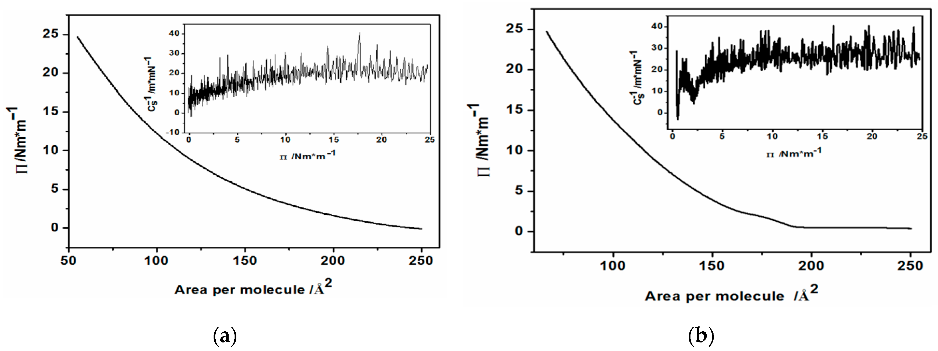
2.3.1. Langmuir Film Formation
2.3.2. Langmuir-Blodgett Film Transfer
2.4. Methods of Characterization
2.5. Photoelectrochemical Measurements
3. Results and Discussion
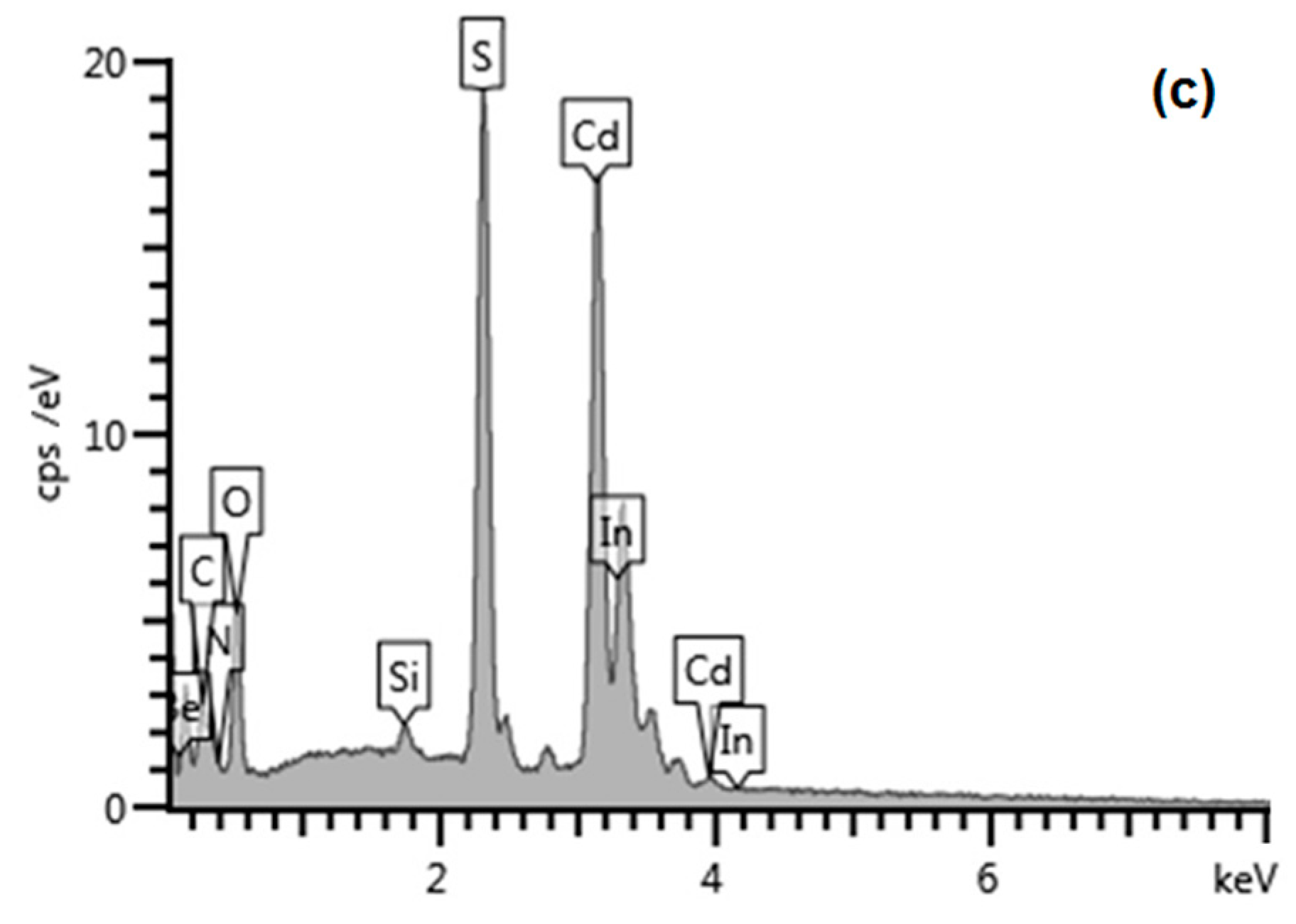
3.1. Physico-Chemical Characteristics of CdS
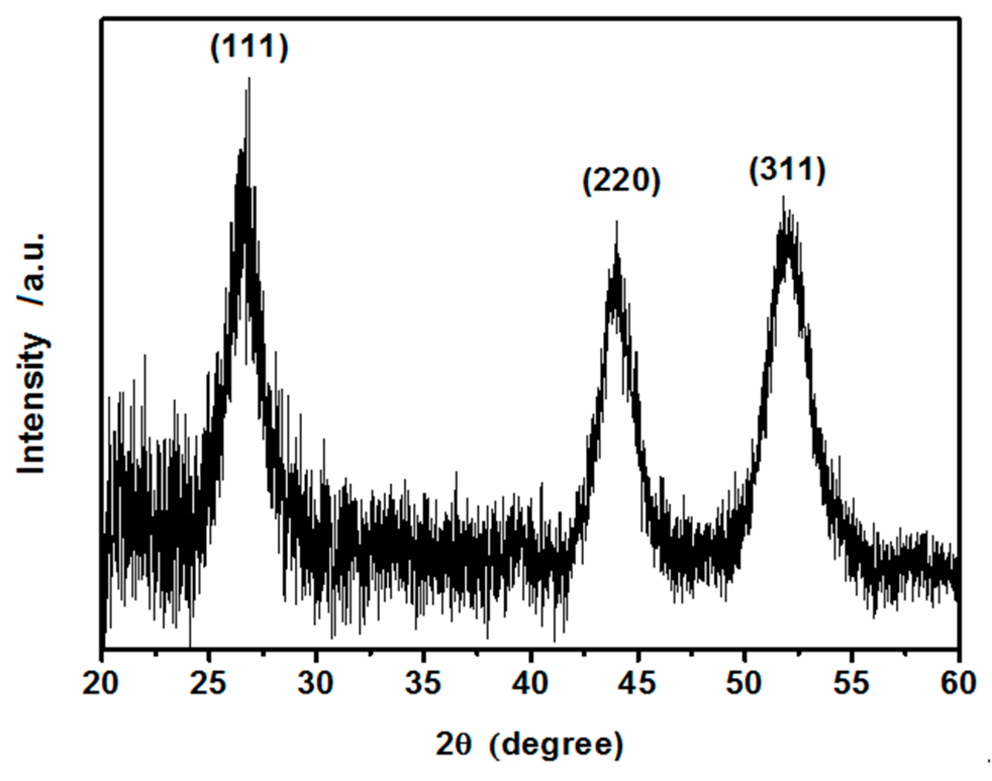
3.1.1. XRD Analysis
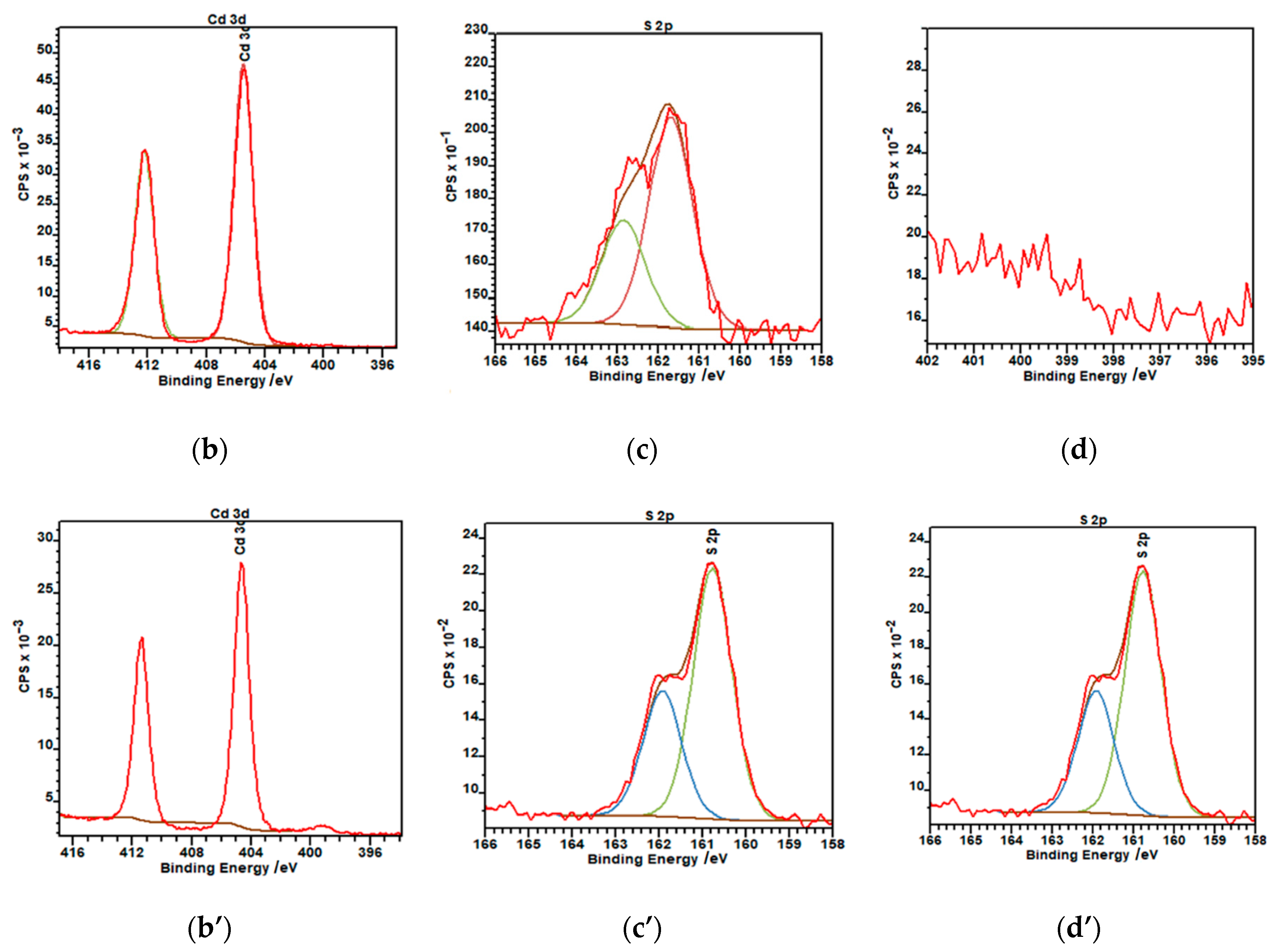
3.1.2. XPS Analysis
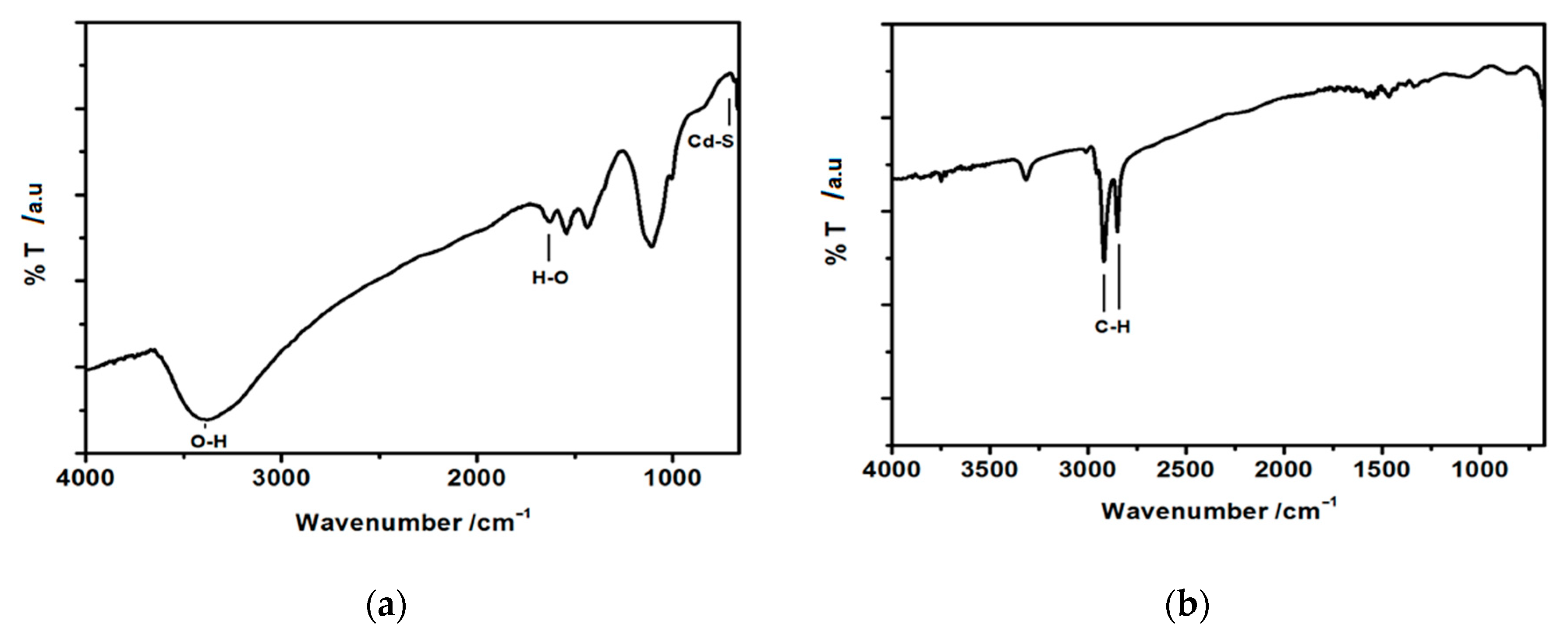
3.1.3. FT-IR Analysis
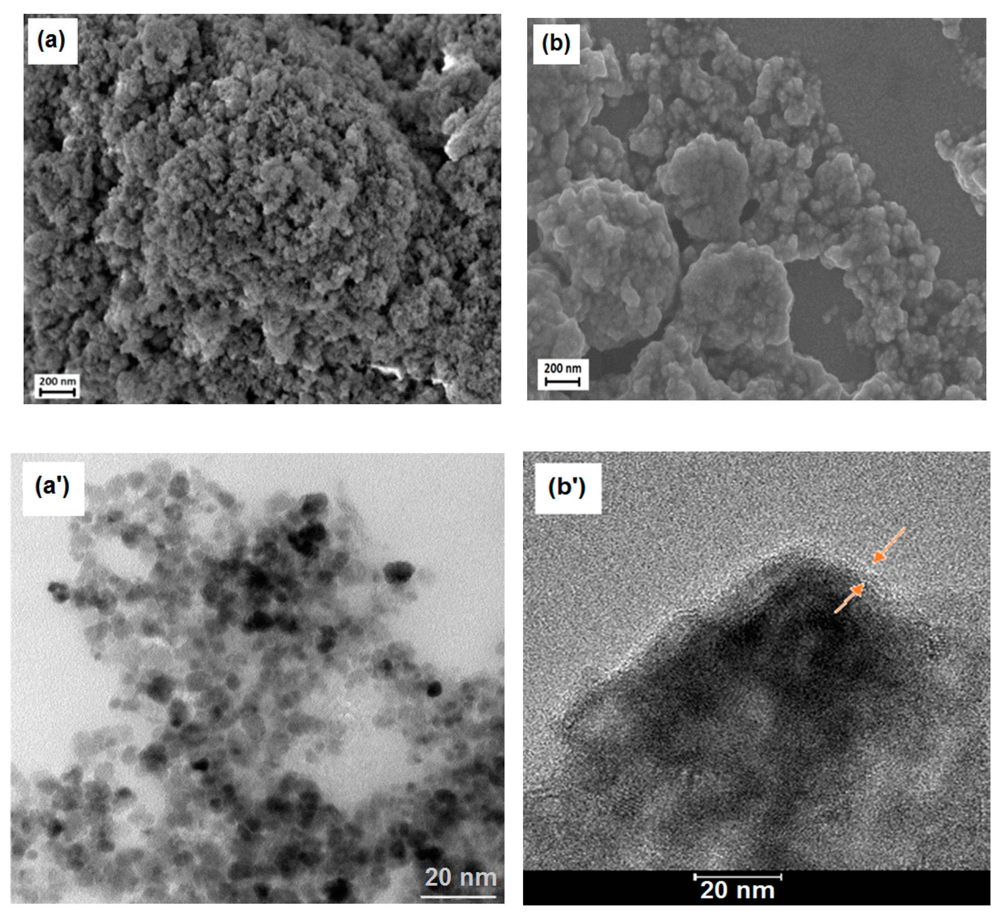
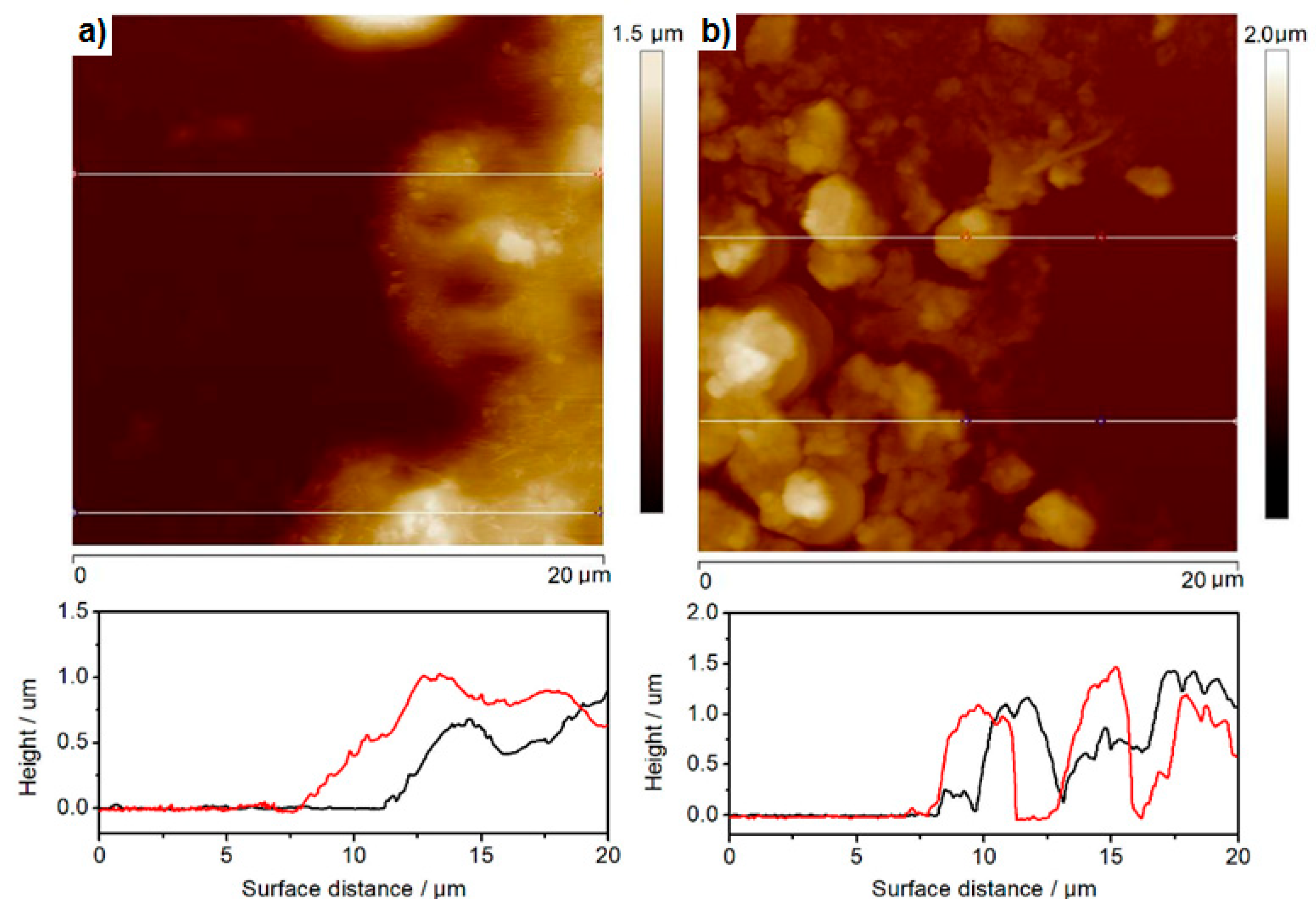
3.2. Morphological Studies of CdS Thin Films
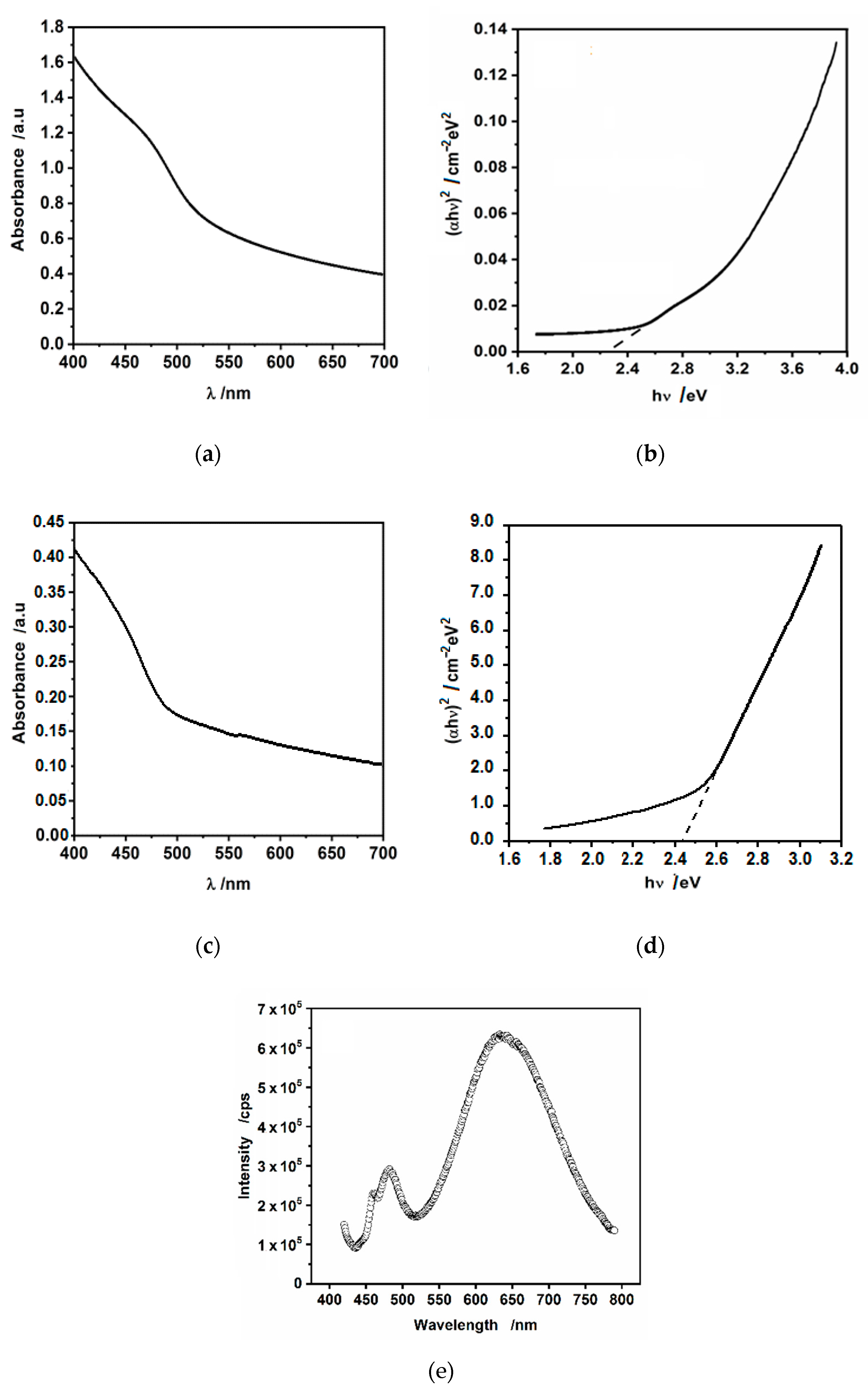
3.3. Optical Absorption and Photoluminescence Studies
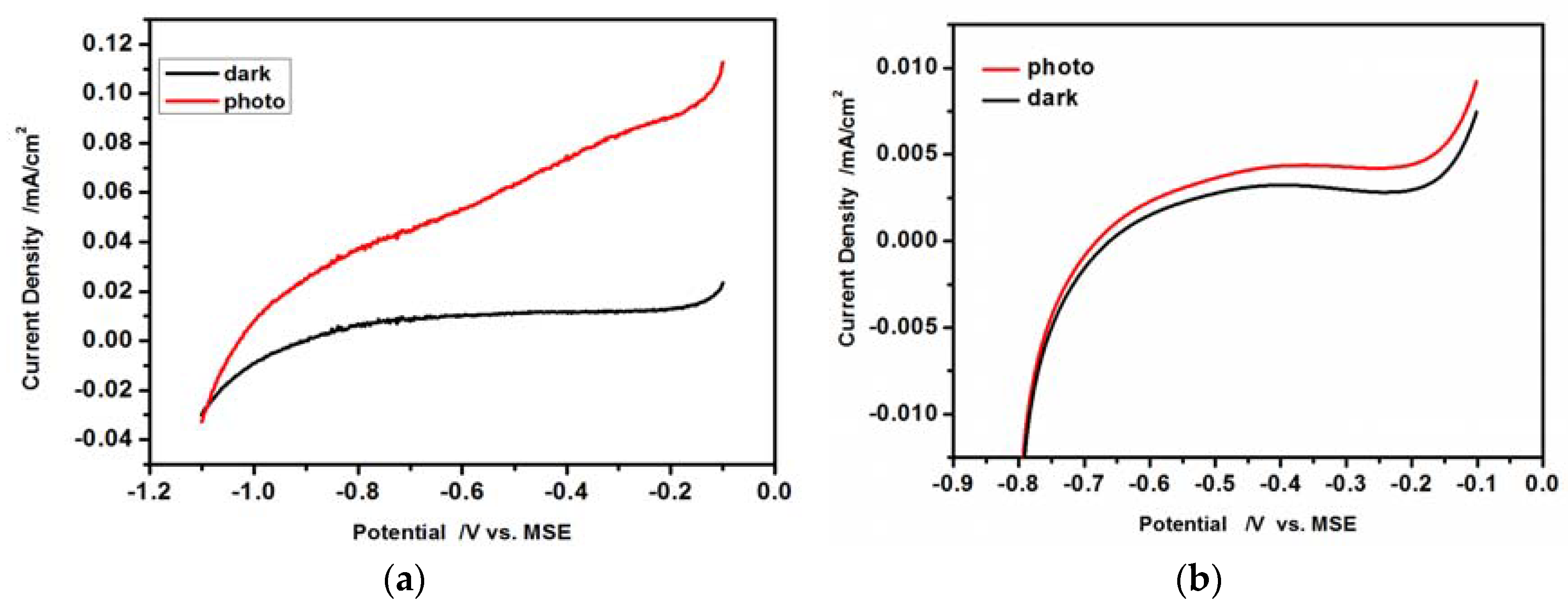
3.4. Photoelectrochemical Features of CdS Drop-Cast Hydrophilic Particles and Hydrophobic CdS Particles in L-B Layers
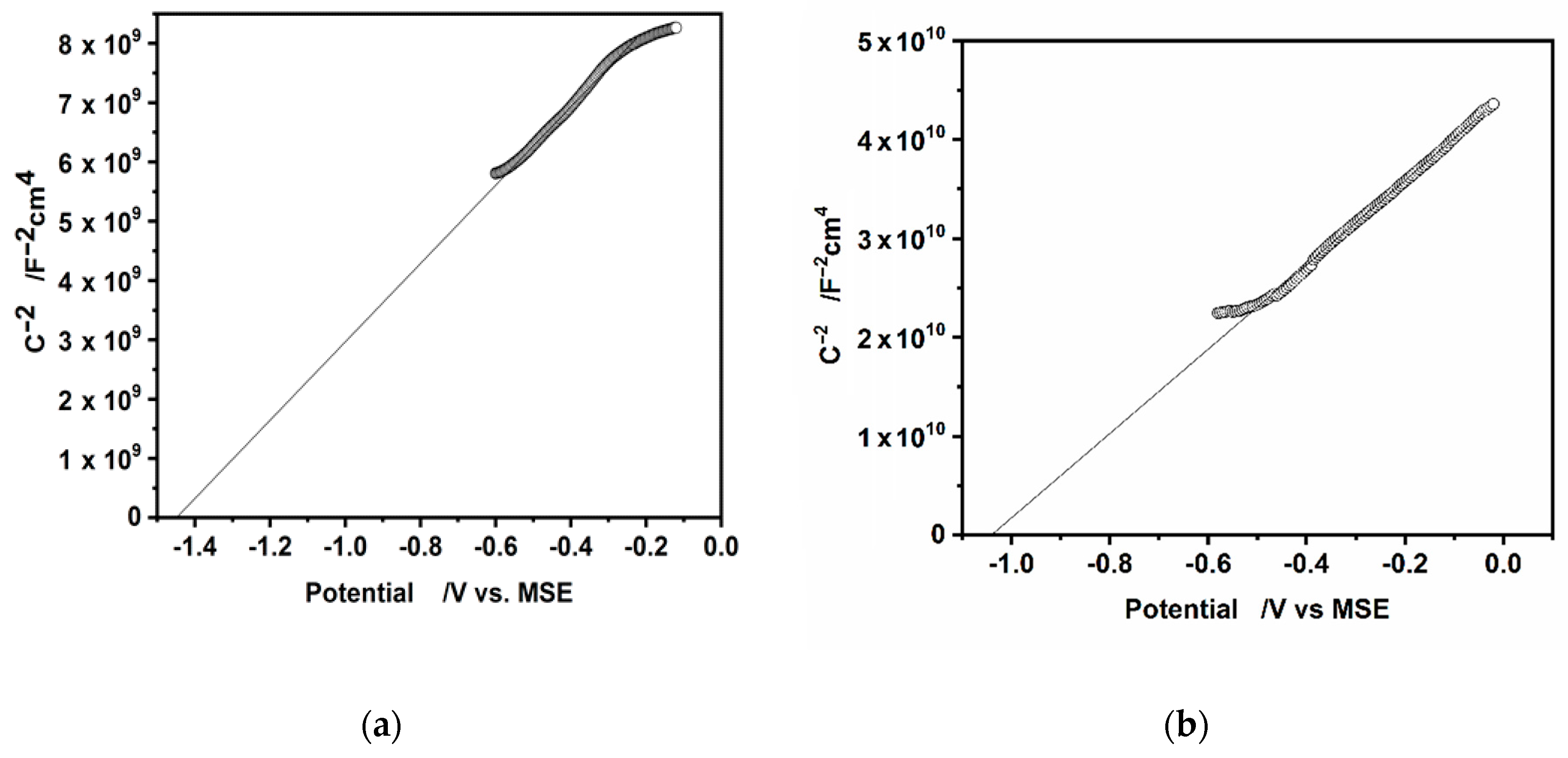
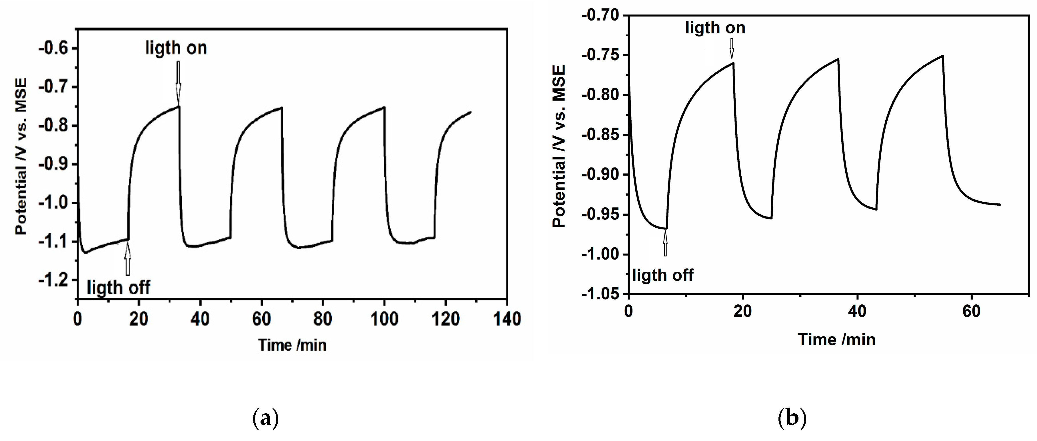
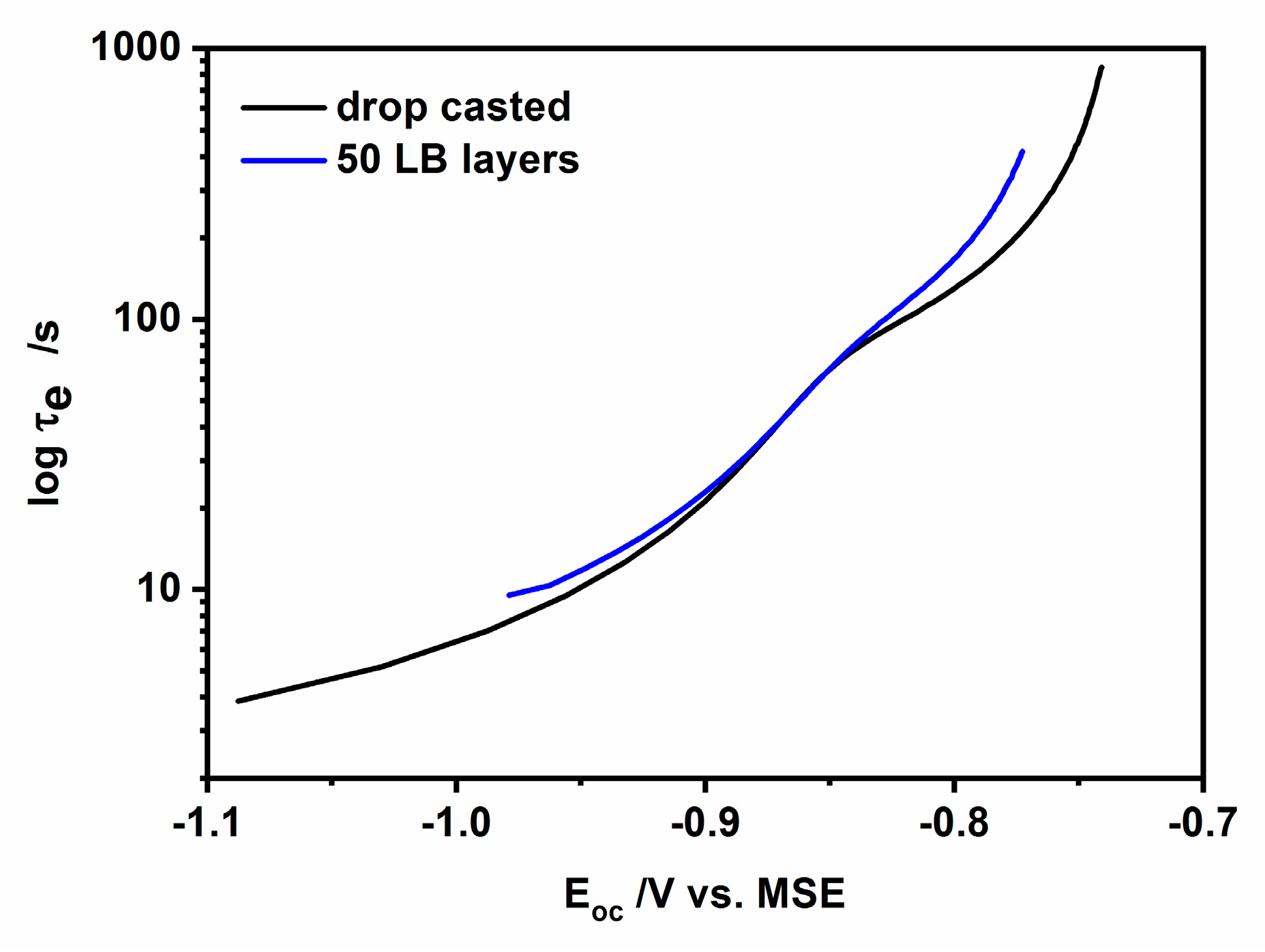
3.5. Open Circuit Photovoltage and Photocurrent Analysis
4. Conclusions
Author Contributions
Funding
Acknowledgments
Conflicts of Interest
References
- Mora-Seró, I.; Bisquert, J. Breakthroughs in the development of semiconductor sensitized solar cells. J. Phys. Chem. Lett. 2010, 1, 3046–3052. [Google Scholar] [CrossRef]
- Wang, M.; Lee, H.; Wang, M.; Chen, P.; Gamelin, D.R.; Zakeeruddin, S.M.; Gra, M.; Nazeeruddin, K. Efficient CdSe quantum dot-sensitized solar cells prepared by an improved successive ionic layer adsorption and reaction process. Nano Lett. 2009, 9, 4221–4227. [Google Scholar] [CrossRef]
- Jin, H.; Choi, S.; Lee, H.J.; Kim, S. Layer-by-layer Assemblies of semiconductor quantum dots for nanostructured photovoltaic devices. J. Phys. Chem. Lett. 2013, 4, 2461–2470. [Google Scholar] [CrossRef]
- Martinez-Alonso, C.; Cortina-Marrero, H.J.; Coria-Monroy, C.S.; Arenas, M.C.; Nicho, M.E.; Hu, H. Solution synthesized CdS nanoparticles for hybrid solar cell applications. J. Mater. Sci. Mater. Electron. 2015, 26, 5539–5545. [Google Scholar] [CrossRef]
- Park, Y.; Kim, E.K.; Lee, S.; Lee, J. Growth and characterization of CdS thin films on polymer substrates for photovoltaic applications. J. Nanosci. Nanotechnol. 2014, 14, 3880–3883. [Google Scholar] [CrossRef]
- Khan, Z.R.; Zulfequar, M.; Khan, M.S. Chemical synthesis of CdS nanoparticles and their optical and dielectric studies. J. Mater. Sci. 2011, 46, 5412–5416. [Google Scholar] [CrossRef]
- Rühle, S.; Shalom, M.; Zaban, A. Quantum-dot-sensitized solar cells. Chem. Phys. Chem. 2010, 11, 2290–2304. [Google Scholar] [CrossRef]
- Yang, Z.; Chen, C.Y.; Roy, P.; Chang, H.T. Quantum dot-sensitized solar cells incorporating nanomaterials. Chem. Commun. 2011, 47, 9561–9571. [Google Scholar] [CrossRef]
- Kamat, P.V. Quantum dot solar cells. The next big thing in photovoltaics. J. Phys. Chem. Lett. 2013, 4, 908–918. [Google Scholar] [CrossRef]
- Pan, Z.; Zhang, H.; Cheng, K.; Hou, Y.; Hua, J.; Zhong, X. Highly efficient inverted type-I CdS/CdSe core/shell structure QD-sentisized solar cells. ACS Nano 2012, 6, 3982–3991. [Google Scholar] [CrossRef]
- Barkhouse, D.A.R.; Pattantyus-Abraham, A.G.; Levina, L.; Sargent, E.H. Thiols passivate recombination centers in colloidal quantum dots leading to enhanced photovoltaic device efficiency. ACS Nano 2008, 2, 2356–2362. [Google Scholar] [CrossRef]
- Zhao, N.; Osedach, T.P.; Chang, L.Y.; Geyer, S.M.; Wanger, D.; Binda, M.T.; Arango, A.C.; Bawendi, M.G.; Bulovic, V. Colloidal PbS quantum dot solar cells with high fill factor. ACS Nano 2010, 4, 3437–3752. [Google Scholar] [CrossRef]
- Ip, A.H.; Thon, S.M.; Hoogland, S.; Voznyy, O.; Zhitomirsky, D.; Debnath, R.; Levina, L.; Rollny, L.R.; Carey, G.H.; Fischer, A.; et al. Hybrid passivated colloidal quantum dot solids. Nat. Nanotechnol. 2012, 7, 577–582. [Google Scholar] [CrossRef]
- Tang, J.; Kemp, K.W.; Hoogland, S.K.; Jeong, S.; Liu, H.; Levina, L.; Furukawa, M.; Wang, X.; Debnath, R.; Cha, D.; et al. Colloidal-quantum-dot photovoltaics using atomic-ligand passivation. Nat. Mater. 2011, 10, 765–771. [Google Scholar] [CrossRef]
- Barea, E.M.; Shalom, M.; Gimenez, S.; Hod, I.; Mora-Sero, I.; Zaban, A.; Bisquert, J. Design of injection and recombination in quantum dot sensitized solar cells. J. Am. Chem. Soc. 2010, 132, 6834–6839. [Google Scholar] [CrossRef]
- Watson, D.F. Linker-assisted assembly and intefacial electron-transfer reactivity of quantum dot—Substrate architecture. J. Phys. Chem. Lett. 2010, 1, 2299–2309. [Google Scholar] [CrossRef]
- Bullen, C.; Mulvaney, P. The effects of chemisorption on the luminescence of CdSe quantum dots. Langmuir 2006, 22, 3007–3013. [Google Scholar] [CrossRef]
- Zamborini, F.P.; Hicks, J.F.; Murray, R.W. Quantized double layer charging of nanoparticle films assembled using carboxylate/[Cu2+ or Zn2+]/carboxylate bridges. J. Am. Chem. Soc. 2000, 122, 4514–4515. [Google Scholar] [CrossRef]
- Rao, C.N.R.; Vivekchand, S.R.C.; Biswas, K.; Govindaraj, A. Synthesis of inorganic nanomaterials. Dalton Trans. 2007, 3728–3749. [Google Scholar] [CrossRef]
- Miao, J.J.; Jiang, L.P.; Liu, C.; Zhu, J.M.; Zhu, J.J. General sacrificial template method for the synthesis of cadmium chalcogenide hollow structures. Inorg. Chem. 2007, 46, 5673–5677. [Google Scholar] [CrossRef]
- Pham, L.Q.; Van, T.K.; Cha, H.G.; Kang, Y.S. Controlling crystal growth orientation and crystallinity of cadmium sulfide nanocrystals in aqueous phase by using cationic surfactant. Cryst. Eng. Comm. 2012, 14, 7888–7890. [Google Scholar] [CrossRef]
- Cai, L.; Wang, W.X.; Jin, L.; Yao, Z.R.; Lin, W.J.; Meng, L.X.; Ai, B.; Liang, Z.C.; Huang, Y.L.; Zhang, F.Q.; et al. 2.29% Low temperature-processed dopant-free CdS/p-Si heterojunction solar cells. Adv. Mater. Interfaces 2019, 6, 1900367. [Google Scholar] [CrossRef]
- Li, D.B.; Yin, X.X.; Grice, C.R.; Guan, L.; Song, Z.N.; Wang, C.L.; Chen, C.; Li, K.H.; Cimaroli, A.J.; Awni, A.R.; et al. Stable and efficient CdS/Sb2Se3 solar cells prepared by scalable close space sublimation. Nano Energy 2018, 48, 346–353. [Google Scholar] [CrossRef]
- Guo, Y.; Wang, J.; Yang, L.; Zhang, J.; Jiang, K.; Li, W.; Wang, L.; Jiang, L. Facile additive-free solvothermal synthesis of cadmium sulfide flower-like three dimensional assemblies with unique optical properties and photocatalytic activity. Cryst. Eng. Comm. 2011, 13, 5045–5048. [Google Scholar] [CrossRef]
- Arora, M.K.; Sahu, N.; Upadhyay, S.N.; Sinha, A.S.K. Activity of cadmium sulfide photocatalysts for hydrogen production from water: Role of support. Ind. Eng. Chem. Res. 1999, 38, 2659–2665. [Google Scholar] [CrossRef]
- Barrelet, C.J.; Wu, Y.; Bell, D.C.; Lieber, C.M. Synthesis of CdS and ZnS nanowires using single-source molecular precursor. J. Am. Chem. Soc. 2003, 125, 11498–11499. [Google Scholar] [CrossRef]
- Thongtem, T.; Phuruangrat, A.; Thongtem, S. Characterization of nano- and micro-crystalline CdS synthesized using cyclic microwave radiation. J. Phys. Chem. Solids 2008, 69, 1346–1349. [Google Scholar] [CrossRef]
- Shen, X.P.; Yuan, A.H.; Wang, F.; Hong, J.M.; Xu, Z. Fabrication of well-aligned CdS nanotubes by CVD-template method. Solid State Commun. 2005, 133, 19–22. [Google Scholar] [CrossRef]
- Ge, J.P.; Li, Y.D. Selective atmospheric pressure chemical vapor deposition route to CdS arrays, nanowires, and nanocombs. Adv. Funct. Mater. 2004, 14, 157–162. [Google Scholar] [CrossRef]
- Yong, K.T.; Sahoo, Y.; Swihart, M.T.; Prasad, P.N. Shape control of CdS nanocrystals in one-pot synthesis. J. Phys. Chem. C 2007, 111, 2447–2458. [Google Scholar] [CrossRef]
- Wu, Y.; Wang, L.; Xiao, M.; Huang, X. A novel sonochemical synthesis and nanostructured assembly of polyvinylpyrrolidone-capped CdS colloidal nanoparticles. J. Non-Cryst. Solids 2008, 354, 2993–3000. [Google Scholar] [CrossRef]
- Dutta, P.; Fendler, J.H. Preparation of cadmium sulfide nanoparticles in self-reproducing reversed micelles. J. Colloid Interface Sci. 2002, 247, 47–53. [Google Scholar] [CrossRef]
- Chen, M.; Kim, Y.N.; Li, C.; Cho, S.O. Controlled synthesis of hyperbranched cadmium sulfide micro/nanocrystals. Cryst. Growth Des. 2008, 8, 629–634. [Google Scholar] [CrossRef]
- Shakouri-Arani, M.; Salavati-Niasari, M. Synthesis and characterization of cadmium sulfide nanocrystals in the presence of a new sulfur source via a simple solvothermal method. New J. Chem. 2014, 38, 1179–1185. [Google Scholar] [CrossRef]
- Kundu, J.; Khilari, S.; Pradhan, D. Shape-dependent photocatalytic activity of hydrothermally synthesized cadmium sulfide nanostructures. ACS Appl. Mater. Interfaces 2017, 9, 9669–9680. [Google Scholar] [CrossRef]
- Thangadurai, P.; Balaji, S.; Manoharan, P.T. Surface modification of CdS quantum dots using thiols—Structural and photophysical studies. Nanotechnology 2008, 19, 435708–435716. [Google Scholar] [CrossRef]
- Reddy, C.V.; Shim, J.; Cho, M. Synthesis, structural, optical and photocatalytic properties of CdS/ZnS core/shell nanoparticles. J. Phys. Chem. Solids 2017, 103, 209–217. [Google Scholar] [CrossRef]
- Huang, L.; Wang, X.; Yang, J.; Liu, G.; Han, J.; Li, C. Dual cocatalysts loaded type I CdS/ZnS core/shell nanocrystals as effective and stable photocatalysts for H2 evolution. J. Phys. Chem. C 2013, 117, 11584–11591. [Google Scholar] [CrossRef]
- Amiri, O.; Mashkani, S.M.H.; Rad, M.M.; Abdvali, F. Sonochemical synthesis and characterization of CdS/ZnS core–shell nanoparticles and application in removal of heavy metals from aqueous solution. Superlattices Microstruct. 2014, 66, 67–75. [Google Scholar] [CrossRef]
- Henglein, A. Small-particle research: Physicochemical properties of extremely small colloidal metal and semiconductor particles. Chem. Rev. 1989, 89, 1861–1873. [Google Scholar] [CrossRef]
- Oliveira, O.N., Jr. Langmuir-Blodgett films—Properties and possible applications. Braz. J. Phys. 1992, 22, 60–69. [Google Scholar]
- Sun, X.; Ma, X.; Bai, L.; Chang, Z.; Evans, D.G.; Duan, Z.; Wang, J.; Chiang, J.F. Nanoseparation-inspired manipulation of the synthesis of CdS nanorods. Nano Res. 2011, 4, 226–232. [Google Scholar] [CrossRef]
- Nagamine, M.; Osial, M.; Jackowska, K.; Krysinski, P.; Widera-Kalinowska, J. Tetracycline photocatalytic degradation under CdS treatment. J. Mater. Sci. Eng. 2020, 8, 483. [Google Scholar] [CrossRef]
- Nabok, A.V.; Richardson, T. Cadmium sulfide nanoparticles in Langmuir-Blodgett films of calixarenes. Langmuir 1997, 13, 3198–3201. [Google Scholar] [CrossRef]
- Veerathangam, K.; Pandian, M.S.; Ramasamy, P. Influence of SILAR deposition cycles in CdS quantum dot-sensitized solar cells. J. Mater. Sci. Mater. Electron. 2018, 29, 7318–7324. [Google Scholar] [CrossRef]
- Weng, Y.C.; Chang, H. Screening and characterization for the optimization of CdS-based photocatalysts. RSC Adv. 2016, 6, 41376–41384. [Google Scholar] [CrossRef]
- Cardona, M.; Weinstein, M.; Wolff, G.A. Ultraviolet reflection spectrum of cubic CdS. Phys. Rev. 1965, 140, 633–637. [Google Scholar] [CrossRef]
- Rajbonghshi, H.; Kalita, D. Morphology-dependent photocatalytic degradation of organic pollutant and antibacterial activity with CdS nanostructures. J. Nanosci. Nanotechnol. 2020, 20, 5885–5895. [Google Scholar] [CrossRef]
- Aruga, T.; Domen, K.; Naito, S.; Onishi, T.; Tamaru, K. The role of sulfite anion as a hole scavenger in the photocatalytic hydrogen formation from water on CdS semiconductor under illumination of visible light. Chem. Lett. 1983, 7, 1037–1040. [Google Scholar] [CrossRef]
- Hunger, T.; Lapicque, F.; Storck, A. Electrochemical oxidation of sulphite ions at graphite electrode. J. Appl. Electrochem. 1991, 21, 588–596. [Google Scholar] [CrossRef]
- Meissner, D.; Memming, R.; Kastening, B. Photoelectrochemistry of cadmium sulfide. 1. Reanalysis of photocorrosion and flat-band potential. J. Phys. Chem. 1988, 92, 3476–3483. [Google Scholar] [CrossRef]
- Minoura, H.; Tsuiki, M. Anodic reactions of several reducing agents on illuminated cadmium sulfide electrode. Electrochim. Acta 1978, 23, 1377–1382. [Google Scholar] [CrossRef]
- Maiorova, T.L.; Klyuev, V.G. Recombination processes in pyrolytic cadmium sulfide films. Semiconductors 2009, 43, 292–296. [Google Scholar] [CrossRef]
- Zaban, A.; Greenshtein, M.; Bisquert, J. Determination of the electron lifetime in nanocrystalline dye solar cells by photovoltage decay measurements. Chem. Phys. Chem. 2003, 4, 859–864. [Google Scholar] [CrossRef] [PubMed]
- Bisquert, J.; Zaban, A.; Greenshtein, M.; Mora-Sero, I. Determination of rate constants for charge transfer and the distribution of semiconductor and electrolyte electronic energy levels in dye-sensitized solar cells by open-circuit photovoltage decay method. J. Am. Chem. Soc. 2004, 126, 13550–13559. [Google Scholar] [CrossRef]
- Peter, L.M. Energetics and kinetics of light-driven oxygen evolution at semiconductor electrodes: The example of hematite. J. Solid State Electrochem. 2013, 17, 315–326. [Google Scholar] [CrossRef]
- Gurudayal, L.; Peter, M.; Wong, L.H.; Abch, F.F. Revealing the influence of doping and surface treatment on the surface carrier dynamics in hematite nanorod photoanodes. ACS Appl. Mater. Interfaces 2017, 9, 41265–41272. [Google Scholar] [CrossRef]
- Colombara, D.; Dale, P.J.G.; Kissling, P.; Peter, L.M.; Tombolato, S. Photoelectrochemical screening of solar cell absorber layers: Electron transfer kinetics and surface stabilization. J. Phys. Chem. C 2016, 120, 15956–15965. [Google Scholar] [CrossRef]


Publisher’s Note: MDPI stays neutral with regard to jurisdictional claims in published maps and institutional affiliations. |
© 2020 by the authors. Licensee MDPI, Basel, Switzerland. This article is an open access article distributed under the terms and conditions of the Creative Commons Attribution (CC BY) license (http://creativecommons.org/licenses/by/4.0/).
Share and Cite
Nagamine, M.; Osial, M.; Widera-Kalinowska, J.; Jackowska, K.; Krysiński, P. Photosensitive Thin Films Based on Drop Cast and Langmuir-Blodgett Hydrophilic and Hydrophobic CdS Nanoparticles. Nanomaterials 2020, 10, 2437. https://doi.org/10.3390/nano10122437
Nagamine M, Osial M, Widera-Kalinowska J, Jackowska K, Krysiński P. Photosensitive Thin Films Based on Drop Cast and Langmuir-Blodgett Hydrophilic and Hydrophobic CdS Nanoparticles. Nanomaterials. 2020; 10(12):2437. https://doi.org/10.3390/nano10122437
Chicago/Turabian StyleNagamine, Momoka, Magdalena Osial, Justyna Widera-Kalinowska, Krystyna Jackowska, and Paweł Krysiński. 2020. "Photosensitive Thin Films Based on Drop Cast and Langmuir-Blodgett Hydrophilic and Hydrophobic CdS Nanoparticles" Nanomaterials 10, no. 12: 2437. https://doi.org/10.3390/nano10122437
APA StyleNagamine, M., Osial, M., Widera-Kalinowska, J., Jackowska, K., & Krysiński, P. (2020). Photosensitive Thin Films Based on Drop Cast and Langmuir-Blodgett Hydrophilic and Hydrophobic CdS Nanoparticles. Nanomaterials, 10(12), 2437. https://doi.org/10.3390/nano10122437