Structure-Property Relationships of 2D Ga/In Chalcogenides


Abstract
1. Introduction
2. Computational Details
3. 2D Layer-Dependent Properties
3.1. Stability and Electronic Property
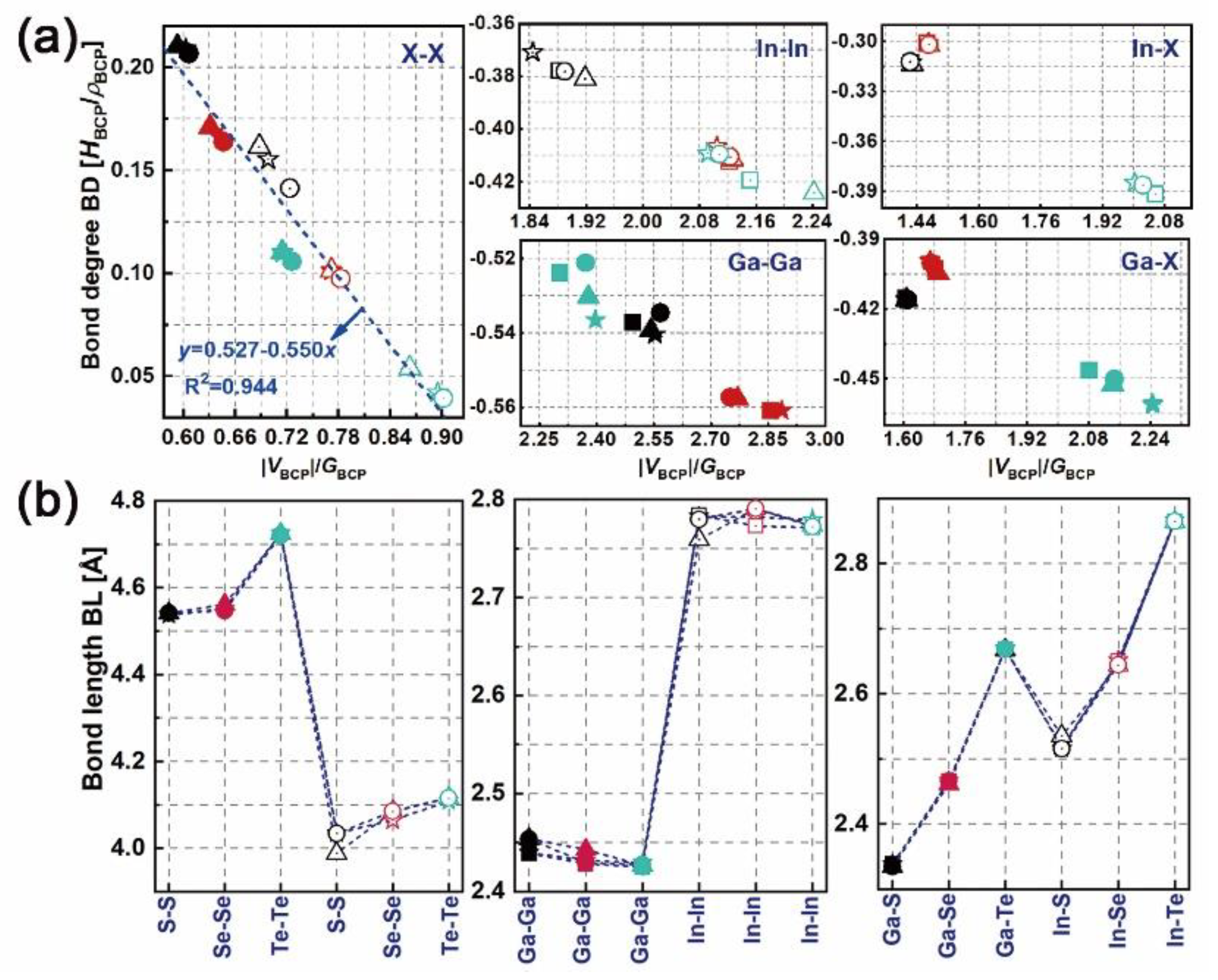
3.2. Topological Properties of Electron Density
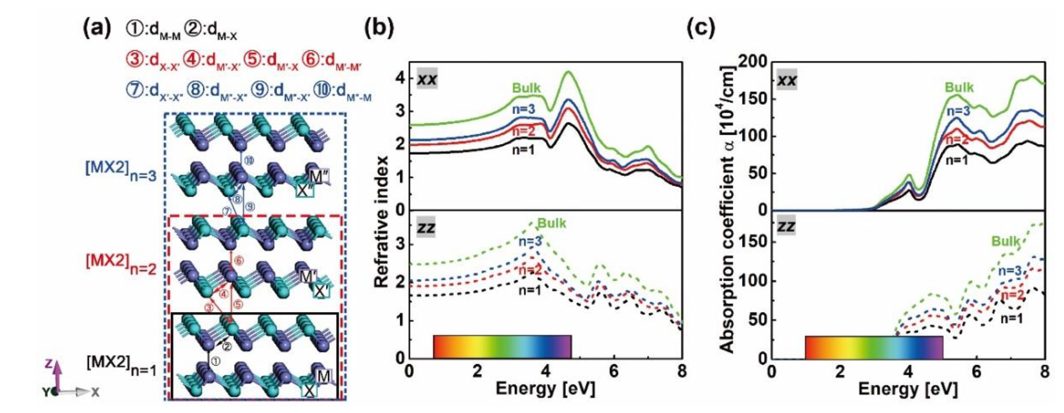
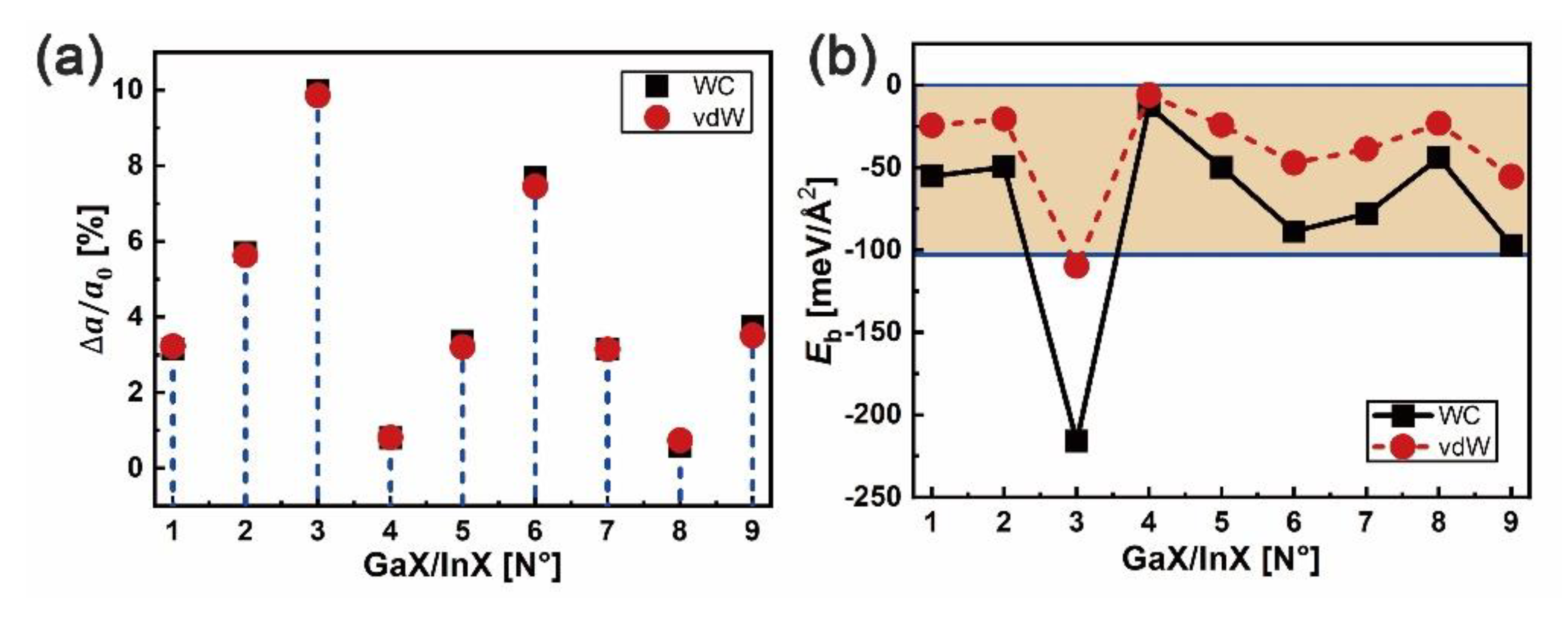
4. Heterostructure Properties
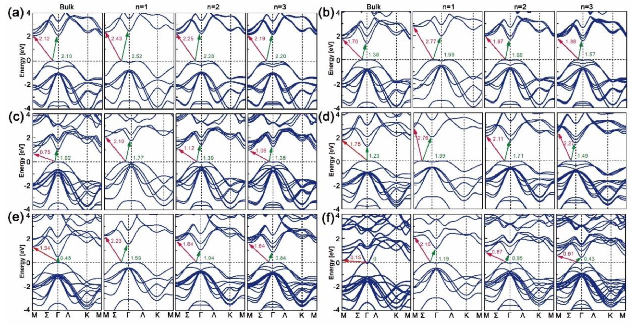
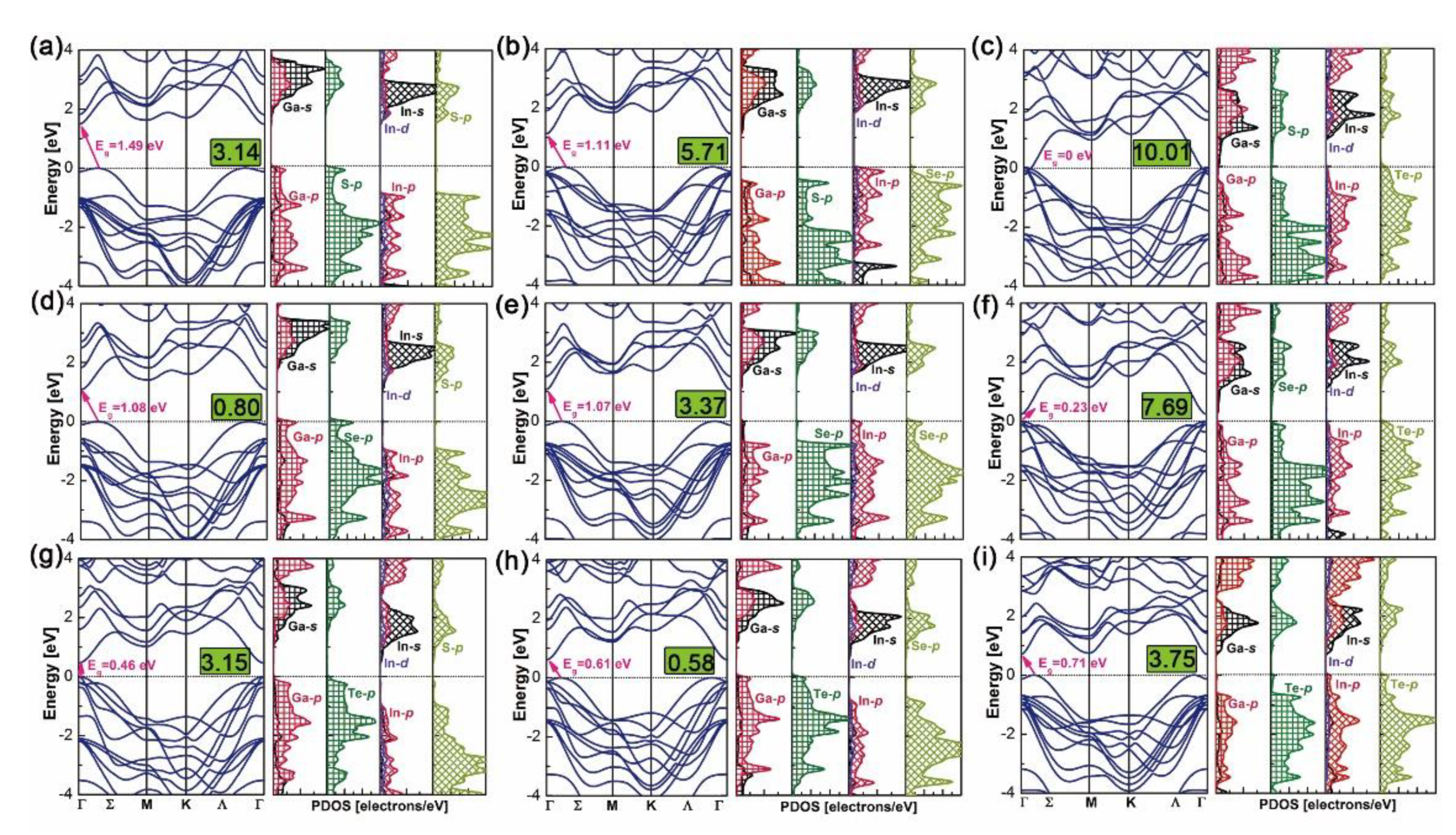
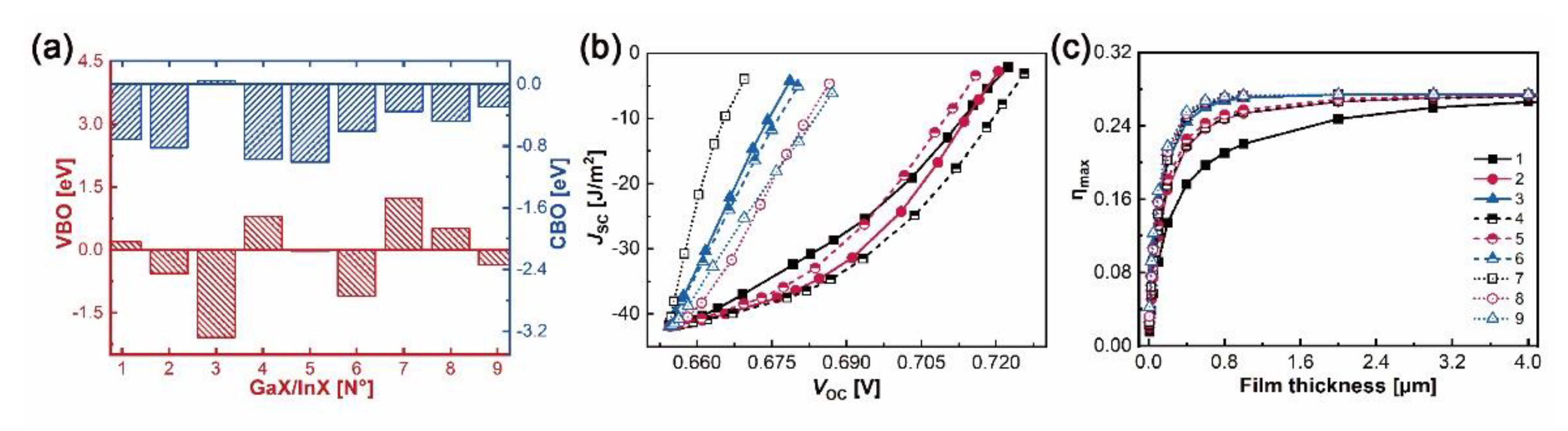
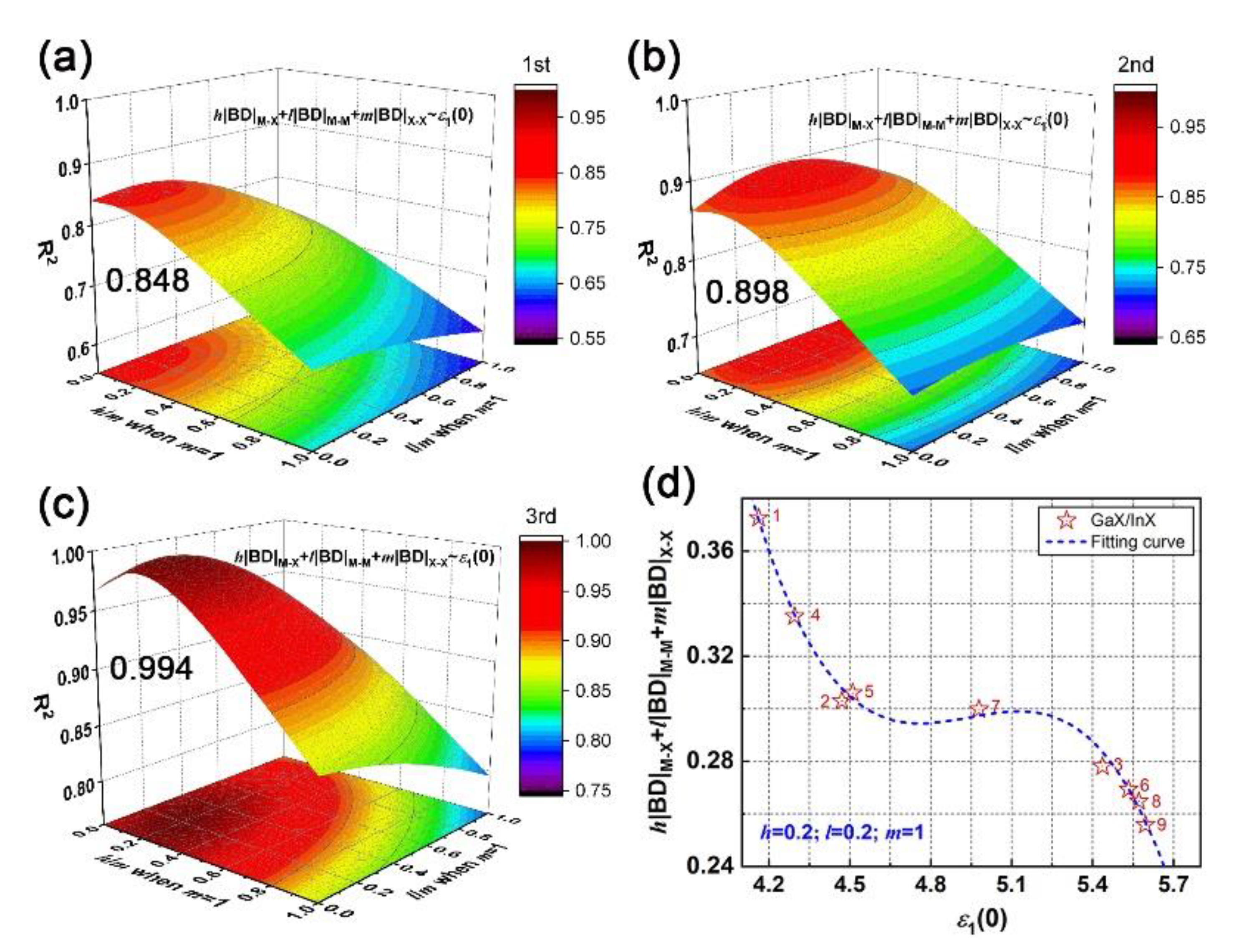
4.1. Stability and Electronic Property
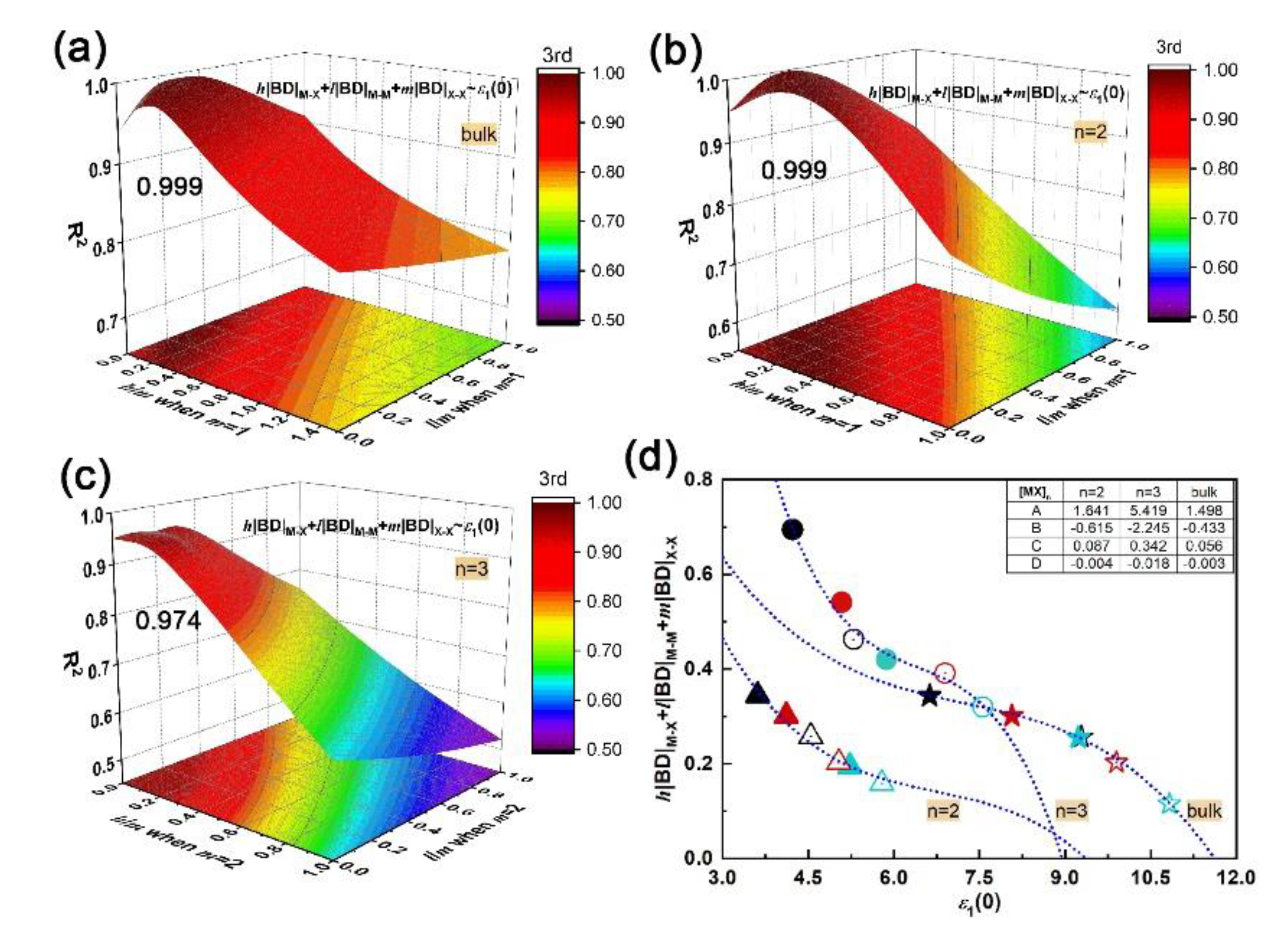
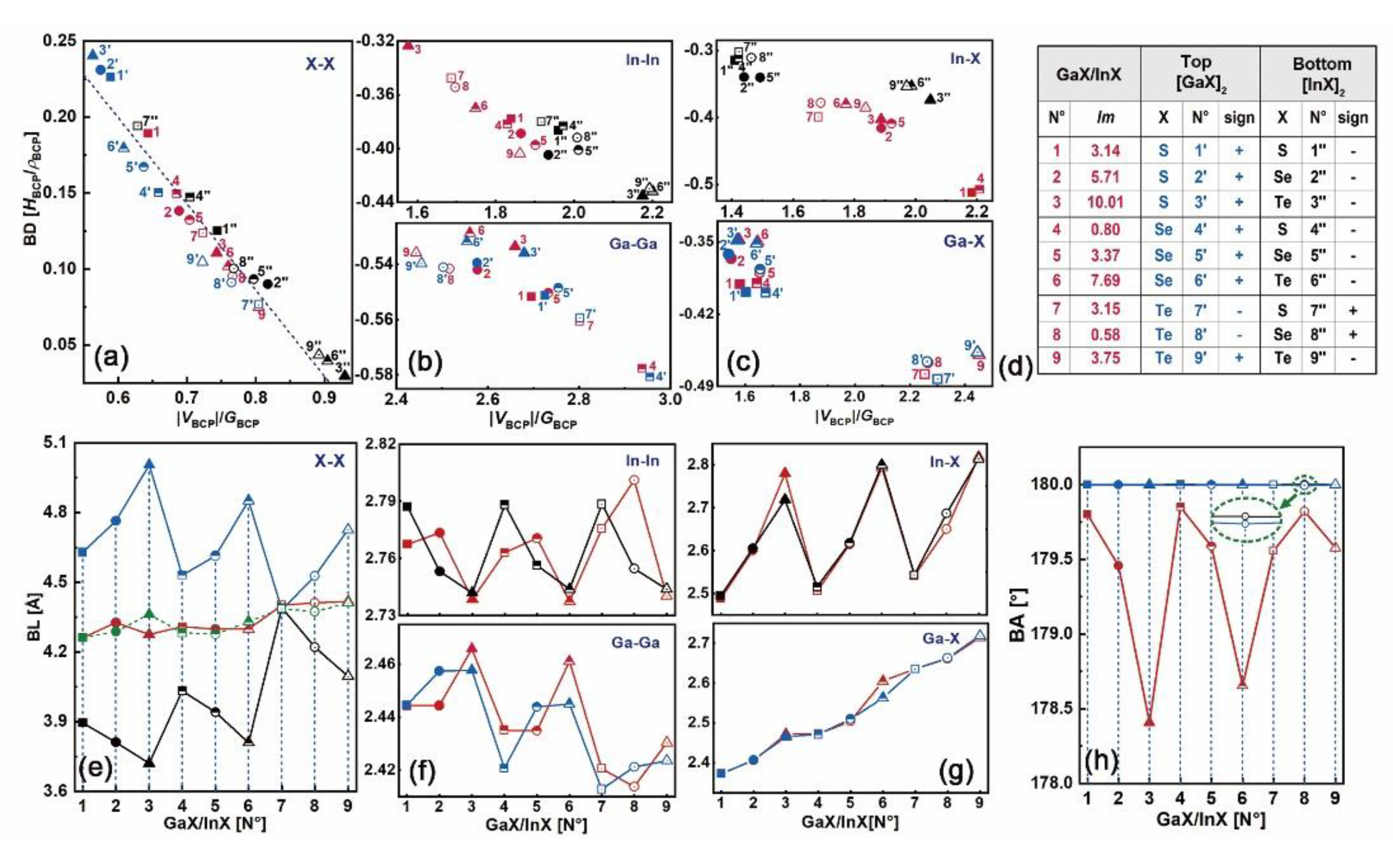
4.2. Topological Properties of Electron Density
5. Conclusions
Supplementary Materials
Author Contributions
Funding
Acknowledgments
Conflicts of Interest
References
- Wang, J.; Bo, W.; Ding, Y.; Mu, X. Optical, optoelectronic and photoelectric properties in Moiré superlattices of twisted bilayer graphene. Mater. Today Phys. 2020, 14, 100238. [Google Scholar] [CrossRef]
- Zhou, X.; Hu, X.; Yu, J.; Liu, S.; Shu, Z.; Zhang, Q.; Li, H.; Ma, Y.; Xu, H.; Zhai, T. 2D Layered Material-Based van der Waals Heterostructures for Optoelectronics. Adv. Funct. Mater. 2018, 28, 1706587. [Google Scholar] [CrossRef]
- Tan, C.; Lai, Z.; Zhang, H. Ultrathin two-dimensional multinary layered metal chalcogenide nanomaterials. Adv. Mater. 2017, 29, 1701392. [Google Scholar] [CrossRef] [PubMed]
- Jariwala, D.; Davoyan, A.R.; Wong, J.; Atwater, H.A. Van der Waals materials for atomically-thin photovoltaics: Promise and outlook. ACS Photonics 2017, 4, 2962–2970. [Google Scholar] [CrossRef]
- Sa, B.; Sun, Z.; Wu, B. The development of two dimensional group IV chalcogenides, blocks for van der Waals heterostructures. Nanoscale 2015, 8, 1169–1178. [Google Scholar] [CrossRef] [PubMed]
- Brahma, M.; Kabiraj, A.; Saha, D.; Mahapatra, S. Scalability assessment of Group-IV mono-chalcogenide based tunnel FET. Sci. Rep. 2018, 8, 5993. [Google Scholar] [CrossRef]
- Jariwala, D.; Marks, T.J.; Hersam, M.C. Mixed-dimensional van der Waals heterostructures. Nature Mater. 2017, 16, 170–181. [Google Scholar] [CrossRef] [PubMed]
- Terrones, H.; López-Urías, F.; Terrones, M. Novel hetero-layered materials with tunable direct band gaps by sandwiching different metal disulfides and diselenides. Sci. Rep. 2013, 3, 1549. [Google Scholar] [CrossRef]
- Gong, C.; Hu, K.; Wang, X.; Wangyang, P.; Yan, C.; Chu, J.; Liao, M.; Dai, L.; Zhai, T.; Wang, C.; et al. 2D Nanomaterial Arrays for Electronics and Optoelectronics. Adv. Funct. Mater. 2018, 28, 1706559. [Google Scholar] [CrossRef]
- Wang, S.; Tian, H.; Ren, C.; Yu, J.; Sun, M. Electronic and optical properties of heterostructures based on transition metal dichalcogenides and graphene-like zinc oxide. Sci. Rep. 2018, 8, 12009. [Google Scholar] [CrossRef]
- Rasmussen, F.A.; Thygesen, K.S. Computational 2D materials database: Electronic structure of transition-metal dichalcogenides and oxides. J. Phys. Chem. C 2015, 119, 13169–13183. [Google Scholar] [CrossRef]
- Zhao, Y.-H.; Yang, F.; Wang, J.; Guo, H.; Ji, W. Continuously tunable electronic structure of transition metal dichalcogenides superlattices. Sci. Rep. 2015, 5, 8356. [Google Scholar] [CrossRef]
- Stanford, M.G.; Pudasaini, P.R.; Belianinov, A.; Cross, N.; Noh, J.H.; Koehler, M.R.; Mandrus, D.G.; Duscher, G.; Rondinone, A.J.; Ivanov, I.N.; et al. Focused helium-ion beam irradiation effects on electrical transport properties of few-layer WSe2: Enabling nanoscale direct write homo-junctions. Sci. Rep. 2016, 6, 27276. [Google Scholar] [CrossRef] [PubMed]
- Zhang, C.; Chuu, C.-P.; Ren, X.; Li, M.-Y.; Li, L.-J.; Jin, C.; Chou, M.-Y.; Shih, C.-K. Interlayer couplings, Moiré patterns, and 2D electronic superlattices in MoS2 /WSe2 hetero-bilayers. Sci. Adv. 2017, 3, e1601459. [Google Scholar] [CrossRef] [PubMed]
- Heo, H.; Sung, J.H.; Cha, S.; Jang, B.-G.; Kim, J.-Y.; Jin, G.; Lee, D.; Ahn, J.-H.; Lee, M.-J.; Shim, J.H.; et al. Interlayer orientation-dependent light absorption and emission in monolayer semiconductor stacks. Nat. Commun. 2015, 6, 7372. [Google Scholar] [CrossRef]
- Chen, J.; He, X.; Sa, B.; Zhou, J.; Xu, C.; Wen, C.; Sun, Z. III–VI van der Waals heterostructures for sustainable energy related applications. Nanoscale 2019, 11, 6431–6444. [Google Scholar] [CrossRef]
- Chen, J.; Tan, X.; Lin, P.; Sa, B.; Zhou, J.; Zhang, Y.; Wen, C.; Sun, Z. Comprehensive understanding of intrinsic mobility in the monolayers of III–VI group 2D materials. Phys. Chem. Chem. Phys. 2019, 21, 21898–21907. [Google Scholar] [CrossRef]
- Chen, J.; Cai, S.; Xiong, R.; Sa, B.; Wen, C.; Wu, B.; Sun, Z. High-performance III–VI monolayer transistors for flexible devices. Phys. Chem. Chem. Phys. 2020, 22, 7039–7047. [Google Scholar] [CrossRef]
- Demirci, S.; Avazlı, N.; Durgun, E.; Cahangirov, S. Structural and electronic properties of monolayer group III monochalcogenides. Phys. Rev. B 2017, 95, 115409. [Google Scholar] [CrossRef]
- Chang, H.-C.; Tu, C.-L.; Lin, K.-I.; Pu, J.; Takenobu, T.; Hsiao, C.-N.; Chen, C.-H. Synthesis of Large-Area InSe Monolayers by Chemical Vapor Deposition. Small 2018, 14, 1802351. [Google Scholar] [CrossRef]
- Zhou, J.; Shi, J.; Zeng, Q.; Chen, Y.; Niu, L.; Liu, F.; Yu, T.; Suenaga, K.; Liu, X.; Lin, J.; et al. InSe monolayer: Synthesis, structure and ultra-high second-harmonic generation. 2D Mater. 2018, 5, 025019. [Google Scholar] [CrossRef]
- Feng, W.; Zheng, W.; Cao, W.; Hu, P. Back gated multilayer InSe transistors with enhanced carrier mobilities via the suppression of carrier scattering from a dielectric interface. Adv. Mater. 2014, 26, 6587–6593. [Google Scholar] [CrossRef]
- Jappor, H.R.; Habeeb, M.A. Optical properties of two-dimensional GaS and GaSe monolayers. Phys. E Low-Dimension. Syst. Nanostruct. 2018, 101, 251–255. [Google Scholar] [CrossRef]
- Ma, Y.; Dai, Y.; Guo, M.; Yu, L.; Huang, B. Tunable electronic and dielectric behavior of GaS and GaSe monolayers. Phys. Chem. Chem. Phys. 2013, 15, 7098. [Google Scholar] [CrossRef] [PubMed]
- Hu, P.; Wang, L.; Yoon, M.; Zhang, J.; Feng, W.; Wang, X.; Wen, Z.; Idrobo, J.C.; Miyamoto, Y.; Geohegan, D.B.; et al. Highly responsive ultrathin GaS nanosheet photodetectors on rigid and flexible Substrates. Nano Lett. 2013, 13, 1649–1654. [Google Scholar] [CrossRef]
- Zhou, Y.; Nie, Y.; Liu, Y.; Yan, K.; Hong, J.; Jin, C.; Zhou, Y.; Yin, J.; Liu, Z.; Peng, H. Epitaxy and photoresponse of two-dimensional GaSe crystals on flexible transparent mica sheets. ACS Nano 2014, 8, 1485–1490. [Google Scholar] [CrossRef]
- Nutting, D.; Felix, J.F.; Tillotson, E.; Shin, D.-W.; De Sanctis, A.; Chang, H.; Cole, N.; Russo, S.; Woodgate, A.; Leontis, I.; et al. Heterostructures formed through abraded van der Waals materials. Nat. Commun. 2020, 11, 3047. [Google Scholar] [CrossRef]
- Phuc, H.V.; Ilyasov, V.V.; Hieu, N.N.; Amin, B.; Nguyen, C.V. Van der Waals graphene/g-GaSe heterostructure: Tuning the electronic properties and Schottky barrier by interlayer coupling, biaxial strain, and electric gating. J. Alloys Compd. 2018, 750, 765–773. [Google Scholar] [CrossRef]
- Mudd, G.W.; Svatek, S.A.; Hague, L.; Makarovsky, O.; Kudrynskyi, Z.R.; Mellor, C.J.; Beton, P.H.; Eaves, L.; Novoselov, K.S.; Kovalyuk, Z.D.; et al. High broad-band photoresponsivity of mechanically formed InSe-graphene van der Waals heterostructures. Adv. Mater. 2015, 27, 3760–3766. [Google Scholar] [CrossRef]
- Jappor, H.R. Electronic structure of novel GaS/GaSe heterostructures based on GaS and GaSe monolayers. Phys. B Condens. Matter 2017, 524, 109–117. [Google Scholar] [CrossRef]
- Bader, R.F.W. A quantum theory of molecular structure and its applications. Chem. Rev. 1991, 91, 893–928. [Google Scholar] [CrossRef]
- Espinosa, E.; Alkorta, I.; Elguero, J.; Molins, E. From weak to strong interactions: A comprehensive analysis of the topological and energetic properties of the electron density distribution involving X–H F–Y systems. J. Chem. Phys. 2002, 117, 5529–5542. [Google Scholar] [CrossRef]
- Yang, H.; Boulet, P.; Record, M.-C. A rapid method for analyzing the chemical bond from energy densities calculations at the bond critical point. Comput. Theor. Chem. 2020, 1178, 112784. [Google Scholar] [CrossRef]
- Blaha, P.; Schwarz, K.; Madsen, G.K.H.; Kvasnicka, D.; Luitz, J.; Laskowsk, R.; Tran, F.; Marks, L.; Marks, L. WIEN2k, an Augmented Plane Wave + Local Orbitals Program for Calculating Crystal Properties Karlheinz Schwarz; Technische Universität Wien: Vienna, Austria, 2001; ISBN 3-9501031-1-2. [Google Scholar]
- Wu, Z.; Cohen, R.E. More accurate generalized gradient approximation for solids. Phys. Rev. B 2006, 73, 235116. [Google Scholar] [CrossRef]
- Tran, F.; Blaha, P. Accurate band gaps of semiconductors and insulators with a semilocal exchange-correlation potential. Phys. Rev. Lett. 2009, 102, 226401. [Google Scholar] [CrossRef]
- Klimeš, J.; Bowler, D.R.; Michaelides, A. Chemical accuracy for the van der Waals density functional. J. Phys. Condens. Matter 2009, 22, 022201. [Google Scholar] [CrossRef]
- Monkhorst, H.J.; Pack, J.D. Special points for Brillouin-zone integrations. Phys. Rev. B 1976, 13, 5188–5192. [Google Scholar] [CrossRef]
- Otero-de-la-Roza, A.; Johnson, E.R.; Luaña, V. Critic2: A program for real-space analysis of quantum chemical interactions in solids. Comput. Phys. Commun. 2014, 185, 1007–1018. [Google Scholar] [CrossRef]
- Jiang, P.; Boulet, P.; Record, M.-C. A DFT study of the electronic, optical and topological properties of free and biaxially strained CuIn1−xAlxSe2. J. Mater. Chem. C 2019, 7, 5803–5815. [Google Scholar] [CrossRef]
- Jiang, P.; Record, M.-C.; Boulet, P. First-principles calculations on CuInSe2/AlP heterostructures. J. Mater. Chem. C 2020, 8, 4732–4742. [Google Scholar] [CrossRef]
- Kuhn, A.; Chevy, A.; Chevalier, R. Refinement of the 2H GaS β-type. Acta Crystallogr. B 1976, 32, 983–984. [Google Scholar] [CrossRef]
- Ho, C.H.; Lin, S.L. Optical properties of the interband transitions of layered gallium sulfide. J. Appl. Phys. 2006, 100, 083508. [Google Scholar] [CrossRef]
- Kuhn, A.; Chevy, A.; Chevalier, R. Crystal structure and interatomic distances in GaSe. Phys. Stat. Sol. (a) 1975, 31, 469–475. [Google Scholar] [CrossRef]
- Chuang, C.-A.; Lin, M.-H.; Yeh, B.-X.; Ho, C.-H. Curvature-dependent flexible light emission from layered gallium selenide crystals. RSC Adv. 2018, 8, 2733–2739. [Google Scholar] [CrossRef]
- Shenoy, U.S.; Gupta, U.; Narang, D.S.; Late, D.J.; Waghmare, U.V.; Rao, C.N.R. Electronic structure and properties of layered gallium telluride. Chem. Phys. Lett. 2016, 651, 148–154. [Google Scholar] [CrossRef]
- Fonseca, J.J.; Tongay, S.; Topsakal, M.; Chew, A.R.; Lin, A.J.; Ko, C.; Luce, A.V.; Salleo, A.; Wu, J.; Dubon, O.D. Bandgap Restructuring of the Layered Semiconductor Gallium Telluride in Air. Adv. Mater. 2016, 28, 6465–6470. [Google Scholar] [CrossRef]
- Pham, K.D.; Vi, V.T.T.; Thuan, D.V.; Phuong, L.T.T.; Hoa, L.T.; Hieu, N.V.; Nguyen, C.V.; Phuc, H.V.; Jappor, H.R.; Cuong, N.Q.; et al. Tunable electronic properties of InSe by biaxial strain: From bulk to single-layer. Mater. Res. Express 2019, 6, 115002. [Google Scholar] [CrossRef]
- Ma, Y.; Dai, Y.; Yu, L.; Niu, C.; Huang, B. Engineering a topological phase transition in β-InSe via strain. New J. Phys. 2013, 15, 073008. [Google Scholar] [CrossRef]
- McCanny, J.V.; Murray, R.B. The band structures of gallium and indium selenide. J. Phys. C Solid State Phys. 1977, 10, 1211–1222. [Google Scholar] [CrossRef]
- Gomes da Costa, P.; Balkanski, M.; Wallis, R.F. Effect of intercalated lithium on the electronic band structure of indium selenide. Phys. Rev. B 1991, 43, 7066–7069. [Google Scholar] [CrossRef]
- Mitroy, J.; Safronova, M.S.; Clark, C.W. Theory and applications of atomic and ionic polarizabilities. J. Phys. B At. Mol. Opt. Phys. 2010, 43, 202001. [Google Scholar] [CrossRef]
- Tessman, J.R.; Kahn, A.H.; Shockley, W. Electronic polarizabilities of ions in crystals. Phys. Rev. 1953, 92, 890–895. [Google Scholar] [CrossRef]
- Zhang, G.-X.; Tkatchenko, A.; Paier, J.; Appel, H.; Scheffler, M. Van der Waals interactions in ionic and semiconductor solids. Phys. Rev. Lett. 2011, 107, 245501. [Google Scholar] [CrossRef]
- Rysselberghe, P.V. Remarks concerning the Clausius-Mossotti Law. J. Phys. Chem. 1932, 36, 1152–1155. [Google Scholar] [CrossRef]
- Atkins, P.W.; De Paula, J. Atkins’ Physical Chemistry, 9th ed.; Oxford University Press: Oxford, UK, 2010; ISBN 978-0-19-954337-3, 972. [Google Scholar]
- Morita, K.; Davies, D.W.; Butler, K.T.; Walsh, A. Modeling the dielectric constants of crystals using machine learning. J. Chem. Phys. 2020, 153, 024503. [Google Scholar] [CrossRef]
- Kowalczyk, S.P.; Cheung, J.T.; Kraut, E.A.; Grant, R.W. CdTe-HgTe (-1-1-1) heterojunction valence-band discontinuity: A common-anion-rule contradiction. Phys. Rev. Lett. 1986, 56, 1605–1608. [Google Scholar] [CrossRef]
- Yu, L.; Zunger, A. Identification of potential photovoltaic absorbers based on first-principles spectroscopic screening of materials. Phys. Rev. Lett. 2012, 108, 068701. [Google Scholar] [CrossRef] [PubMed]


| MX | a (Å) | c (Å) | Eg (eV) | |||||||
|---|---|---|---|---|---|---|---|---|---|---|
| WC-GGA | optB88-vdW | Calc. & Exp. | WC-GGA | optB88-vdW | Calc. & Exp. | WC-GGA | optB88-vdW | mBJ | Calc. & Exp. | |
| GaS | 3.588 | 3.640 | 3.583 (c) [24] 3.587 (e) [42] | 14.935 | 14.932 | 15.531 (c) [24] 15.492 (e) [42] | 2.100 | 1.813 | 2.824 | 1.605 (c) [24] 2.530 (e) [43] |
| GaSe | 3.760 | 3.821 | 3.751 (c) [24] 3.752 (e) [44] | 15.488 | 15.467 | 15.948 (c) [24] 15.940 (e) [44] | 1.384 | 1.095 | 2.476 | 0.995 (c) [24] 2.005 (e) [45] |
| GaTe | 4.069 | 4.136 | 4.040 (c) [46] 4.060 (e) [46] | 15.364 | 15.412 | 16.620 (c) [46] 16.960 (e) [46] | 0.746 | 0.637 | 1.428 | 1.604 (c) [46] 1.650 (e) [47] |
| InS | 3.820 | 3.884 | - | 14.238 | 14.253 | - | 1.226 | 0.960 | 2.313 | - |
| InSe | 4.022 | 4.075 | 3.940 (c) [48] 4.050 (e) [49] | 15.113 | 15.085 | 16.850 (c) [48] 16.930 (e) [49] | 0.484 | 0.367 | 1.449 | 1.2 (c) [50] 1.3 (e) [51] |
| InTe | 4.385 | 4.437 | - | 15.043 | 15.058 | - | 0.000 | 0.138 | 0.786 | - |
| [MX]n | Eform (eV/motif) | N°⑤ (mÅ) | N°⑨ (mÅ) | |||
|---|---|---|---|---|---|---|
| n = 1 | n = 2 | n = 3 | bulk | ∆d2,bulk | ∆d3,bulk | |
| GaS | −3.825 | −7.655 | −11.481 | −7.611 | −1.2 | −20.7 |
| GaSe | −1.684 | −3.385 | −5.105 | −3.452 | −2.0 | −7.5 |
| GaTe | −2.746 | −0.691 | −1.615 | −1.823 | −12.3 | −29.4 |
| InS | −3.637 | −7.270 | −10.913 | −7.304 | −0.8 | −40.7 |
| InSe | −2.235 | −4.508 | −6.788 | −4.505 | 3.8 | 0.8 |
| InTe | −3.370 | −6.150 | −9.776 | −6.247 | −10.4 | −10.4 |
Publisher’s Note: MDPI stays neutral with regard to jurisdictional claims in published maps and institutional affiliations. |
© 2020 by the authors. Licensee MDPI, Basel, Switzerland. This article is an open access article distributed under the terms and conditions of the Creative Commons Attribution (CC BY) license (http://creativecommons.org/licenses/by/4.0/).
Share and Cite
Jiang, P.; Boulet, P.; Record, M.-C. Structure-Property Relationships of 2D Ga/In Chalcogenides. Nanomaterials 2020, 10, 2188. https://doi.org/10.3390/nano10112188
Jiang P, Boulet P, Record M-C. Structure-Property Relationships of 2D Ga/In Chalcogenides. Nanomaterials. 2020; 10(11):2188. https://doi.org/10.3390/nano10112188
Chicago/Turabian StyleJiang, Pingping, Pascal Boulet, and Marie-Christine Record. 2020. "Structure-Property Relationships of 2D Ga/In Chalcogenides" Nanomaterials 10, no. 11: 2188. https://doi.org/10.3390/nano10112188
APA StyleJiang, P., Boulet, P., & Record, M.-C. (2020). Structure-Property Relationships of 2D Ga/In Chalcogenides. Nanomaterials, 10(11), 2188. https://doi.org/10.3390/nano10112188