Grain-Boundary-Induced Alignment of Block Copolymer Thin Films


Abstract
1. Introduction
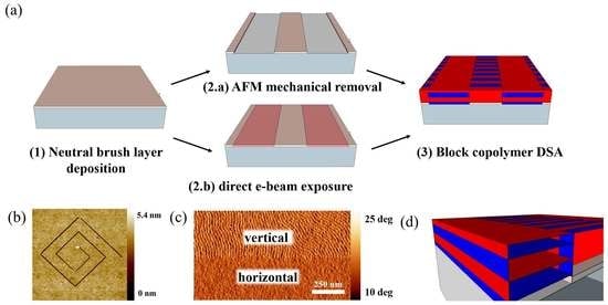
2. Results
2.1. Alignment Induced via Mechanical AFM (m-AFM)
2.2. Alignment Induced via Electron Beam Direct Exposure
2.3. Results of Pattern Transfer of Directed Features into Silicon
3. Discussion
3.1. Surface Energy Modification by m-AFM
3.2. Limits of Grain-Boundary-Induced Alignment
3.3. Fabrication of Patterns of Arbitrary Geometry
4. Materials and Methods
4.1. Substrate
4.2. Neutral Brush Layer Deposition
4.3. Guiding Pattern Fabrication
4.4. Block Copolymer Deposition
4.5. Pattern Transfer
4.6. GISAXS Measurements
5. Conclusions
Author Contributions
Funding
Acknowledgments
Conflicts of Interest
Appendix A
Appendix A.1. Overview of Grain Boundary Morphologies in Block Copolymers


Appendix A.2. Fixed-Height Self-Assembly

Appendix A.3. Grain-Boundary-Induced Alignment with Ternary Blends

References
- Bates, F.S.; Fredrickson, G.H. Block Copolymers—Designer Soft Materials. Phys. Today 1999, 52, 32–38. [Google Scholar] [CrossRef]
- Yang, X.; Xiao, S.; Hu, W.; Hwu, J.; Van De Veerdonk, R.; Wago, K.; Lee, K.; Kuo, D. Integration of nanoimprint lithography with block copolymer directed self-assembly for fabrication of a sub-20 nm template for bit-patterned media. Nanotechnology 2014, 25, 1–11. [Google Scholar] [CrossRef] [PubMed]
- Ruiz, R.; Dobisz, E.; Albrecht, T.R. Rectangular Patterns Using Block Copolymer Directed Assembly for High Bit Aspect Ratio Patterned Media. ACS Nano 2011, 5, 79–84. [Google Scholar] [CrossRef] [PubMed]
- Griffiths, R.A.; Williams, A.; Oakland, C.; Roberts, J.; Vijayaraghavan, A.; Thomson, T. Directed self-assembly of block copolymers for use in bit patterned media fabrication. J. Phys. D Appl. Phys. 2013, 46, 1–29. [Google Scholar] [CrossRef]
- Tsai, H.; Pitera, J.W.; Miyazoe, H.; Bangsaruntip, S.; Engelmann, S.U.; Liu, C.C.; Cheng, J.Y.; Bucchignano, J.J.; Klaus, D.P.; Joseph, E.A.; et al. Two-dimensional pattern formation using graphoepitaxy of PS-b-PMMA block copolymers for advanced FinFET device and circuit fabrication. ACS Nano 2014, 8, 5227–5232. [Google Scholar] [CrossRef]
- Yi, H.; Bao, X.Y.; Tiberio, R.; Wong, H.S.P. A general design strategy for block copolymer directed self-assembly patterning of integrated circuits contact holes using an alphabet approach. Nano Lett. 2015, 15, 805–812. [Google Scholar] [CrossRef]
- Li, W.; Müller, M. Defects in the Self-Assembly of Block Copolymers and Their Relevance for Directed Self-Assembly. Annu. Rev. Chem. Biomol. Eng. 2015, 6, 187–216. [Google Scholar] [CrossRef]
- Neisser, M.; Wurm, S. ITRS lithography roadmap: 2015 challenges. Adv. Opt. Technol. 2015, 4, 235–240. [Google Scholar] [CrossRef]
- Yoshida, A.; Yoshimoto, K.; Ohshima, M. Effect of wall potential on morphology of symmetric diblock copolymers in nanotrench. Jpn. J. Appl. Phys. 2016, 55, 06GE01. [Google Scholar] [CrossRef]
- Chen, W.; Luo, J.; Shi, P.; Li, C.; He, X.; Hong, P.; Li, J.; Zhao, C. Self-assembling morphologies of symmetrical PS b-PMMA in different sized confining grooves. RSC Adv. 2014, 4, 50393–50400. [Google Scholar] [CrossRef]
- Han, B.E.; Kang, H.; Liu, C.; Nealey, P.F.; Gopalan, P. Graphoepitaxial Assembly of Symmetric Block Copolymers on Weakly Preferential Substrates. Adv. Mater. 2010, 22, 4325–4329. [Google Scholar] [CrossRef] [PubMed]
- Borah, D.; Rassapa, S.; Shaw, M.T.; Hobbs, R.G.; Petkov, N.; Schmidt, M.; Holmes, J.D.; Morris, M. Directed self-assembly of PS-b-PMMA block copolymer using HSQ lines for translational alignment. J. Mater. Chem. C 2013, 1, 1192–1196. [Google Scholar] [CrossRef]
- Ilievski, F.; Ross, C.A. Graphoepitaxy of block copolymers using selectively removable templates. J. Vac. Sci. Technol. A 2010, 28, 42–44. [Google Scholar] [CrossRef]
- Borah, D.; Cummins, C.; Rasappa, S.; Senthamaraikannan, R.; Salaun, M.; Zelsmann, M.; Liontos, G.; Ntetsikas, K.; Avgeropoulos, A.; Morris, M.A. Nanopatterning via self-assembly of a lamellar-forming polystyrene-block-poly(Dimethylsiloxane) diblock copolymer on topographical substrates fabricated by nanoimprint lithography. Nanomaterials 2018, 8, 32. [Google Scholar] [CrossRef] [PubMed]
- Walton, D.; Kellogg, G.J.; Mayes, A.; Lambooy, P.; Russell, T.P. A Free Energy Model for Confined Diblock Copolymers. Macromolecules 1994, 27, 6225–6228. [Google Scholar] [CrossRef]
- Turner, M.S. Equilibrium Properties of a Diblock Copolymer Lamellar Phase Confined between Flat Plates. Phys. Rev. Lett. 1992, 69, 1788–1791. [Google Scholar] [CrossRef] [PubMed]
- Gottlieb, S.; Kazazis, D.; Mochi, I.; Evangelio, L.; Fernández-Regúlez, M.; Ekinci, Y.; Perez-Murano, F. Nano-confinement of block copolymers in high accuracy topographical guiding patterns: Modelling the emergence of defectivity due to incommensurability. Soft Matter 2018, 14. [Google Scholar] [CrossRef]
- Cummins, C.; Bell, A.; Morris, M. Creating Active Device Materials for Nanoelectronics Using Block Copolymer Lithography. Nanomaterials 2017, 7, 304. [Google Scholar] [CrossRef]
- Borah, D.; Shaw, M.T.; Holmes, J.D.; Morris, M.A. Sub-10 nm Feature Size PS-b-PDMS Block Copolymer Structures Fabricated by a Microwave-Assisted Solvothermal Process. ACS Appl. Mater. Interfaces 2013, 5, 2004–2012. [Google Scholar] [CrossRef]
- Nickmans, K.; Murphy, J.N.; De Waal, B.; Leclère, P.; Doise, J.; Gronheid, R.; Broer, D.J.; Schenning, A.P.H.J. Sub-5 nm Patterning by Directed Self-Assembly of Oligo (Dimethylsiloxane) Liquid Crystal Thin Films. Adv. Mater. 2016, 28, 10068–10072. [Google Scholar] [CrossRef]
- Kim, S.O.; Solak, H.H.; Stoykovich, M.P.; Ferrier, N.J.; De Pablo, J.J.; Nealey, P.F. Epitaxial self-assembly of block copolymers on lithographically defined nanopatterned substrates. Nature 2003, 424, 411–414. [Google Scholar] [CrossRef] [PubMed]
- Liu, C.C.; Han, E.; Onses, M.S.; Thode, C.J.; Ji, S.; Gopalan, P.; Nealey, P.F. Fabrication of lithographically defined chemically patterned polymer brushes and mats. Macromolecules 2011, 44, 1876–1885. [Google Scholar] [CrossRef]
- Evangelio Araujo, L. Directed Self-Assembly of Block Copolymers on Chemically Nano-Patterned Surfaces. Ph.D. Thesis, Universitat Autònoma de Barcelona, Barcelona, Spain, 2017. [Google Scholar]
- Ruiz, R.; Kang, H.; Detcheverry, F.A.; Dobisz, E.; Kercher, D.S.; Albrecht, T.R.; de Pablo, J.J.; Nealey, P.F. Density Multiplication and Improved Lithography by Directed Block Copolymer Assembly. Science 2008, 321, 936–939. [Google Scholar] [CrossRef] [PubMed]
- Garner, G.; Williamson, L.; Seidel, R.; Rincon Delgadillo, P.; Hur, S.-M.; Gronheid, R.; Nealey, P.F.; de Pablo, J.J. The effects of geometry and chemistry of nanopatterned substrates on the directed self-assembly of block-copolymer melts. Proc. SPIE 2015, 9423, 1–9. [Google Scholar] [CrossRef]
- Evangelio, L.; Fernández-Regúlez, M.; Fraxedas, J.; Müller, M.; Pérez-Murano, F. Role of Penetrability into a Brush-Coated Surface in Directed Self-Assembly of Block Copolymers. ACS Appl. Mater. Interfaces 2018, 11, 3571–3581. [Google Scholar] [CrossRef]
- Thomas, E.L.; Anderson, D.M.; Henkee, C.S.; Hoffman, D. Periodic area-minimizing surfaces in block copolymers. Nature 1988, 334, 598–601. [Google Scholar] [CrossRef]
- Burgaz, E.; Gido, S.P. T-Junction Grain Boundaries in Block Copolymer—Homopolymer Blends. Macromolecules 2000, 33, 8739–8745. [Google Scholar] [CrossRef]
- Jinnai, H.; Sawa, K.; Nishi, T. Direct observation of twisted grain boundary in a block copolymer lamellar nanostructure. Macromolecules 2006, 39, 5815–5819. [Google Scholar] [CrossRef]
- Ryu, H.J.; Fortner, D.B.; Lee, S.; Ferebee, R.; De Graef, M.; Misichronis, K.; Avgeropoulos, A.; Bockstaller, M.R. Role of grain boundary defects during grain coarsening of lamellar block copolymers. Macromolecules 2013, 46, 204–215. [Google Scholar] [CrossRef]
- Gido, S.P.; Thomas, E.L. Lamellar Diblock Copolymer Grain Boundary Morphology. 2. Scherk Twist Boundary Energy Calculations. Macromolecules 1994, 27, 849–861. [Google Scholar] [CrossRef]
- Gido, S.P.; Thomas, E.L. Lamellar Diblock Copolymer Grain Boundary Morphology. 3. Helicoid Section Twist Boundary Energy. Macromolecules 1997, 30, 3739–3746. [Google Scholar] [CrossRef]
- Gido, S.P.; Thomas, E.L. Lamellar Diblock Copolymer Grain Boundary Morphology. 4. Tilt Boundaries. Macromolecules 1994, 27, 6137–6144. [Google Scholar] [CrossRef]
- Gido, S.P.; Gunther, J.; Thomas, E.L.; Hoffman, D. Lamellar diblock copolymer grain boundary morphology. 1. Twist boundary characterization. Macromolecules 1993, 26, 4506–4520. [Google Scholar] [CrossRef]
- Liu, G.; Ramirez-Hernandez, A.; Yoshida, H.; Nygard, K.; Satapathy, D.K.; Bunk, O.; de Pablo, J.; Nealey, P.F. Morphology of Lamellae-Forming Block Copolymer Films between Two Orthogonal Chemically Nanopatterned Striped Surfaces. Phys. Rev. Lett. 2012, 108, 65502. [Google Scholar] [CrossRef]
- Jeong, S.J.; Moon, H.S.; Shin, J.; Kim, B.H.; Shin, D.O.; Kim, J.Y.; Lee, Y.H.; Kim, J.U.; Kim, S.O. One-dimensional metal nanowire assembly via block copolymer soft graphoepitaxy. Nano Lett. 2010, 10, 3500–3505. [Google Scholar] [CrossRef]
- Raybin, J.; Ren, J.; Chen, X.; Gronheid, R.; Nealey, P.F.; Sibener, S.J. Real-Time Atomic Force Microscopy Imaging of Block Copolymer Directed Self Assembly. Nano Lett. 2017, 17, 7717–7723. [Google Scholar] [CrossRef]
- Oria, L.; Ruiz de Luzuriaga, A.; Alduncín, J.A.; Pérez-Murano, F. Block co-polymer guided self-assembly by surface chemical modification: Optimization of multiple patterning process and pattern transfer. Proc. SPIE 2012, 8323, 832327. [Google Scholar] [CrossRef]
- Duque, D.; Katsov, K.; Schick, M. Theory of T junctions and symmetric tilt grain boundaries in pure and mixed polymer systems. J. Chem. Phys. 2002, 117, 10315–10320. [Google Scholar] [CrossRef]
- Stoykovich, M.P.; Muller, M.; Kim, S.O.; Solak, H.H.; Edwards, E.W.; de Pablo, J.J.; Nealey, P.F. Directed assembly of block copolymer blends into nonregular device-oriented structures. Science 2005, 308, 1442–1446. [Google Scholar] [CrossRef]
- Murphy, J.N.; Harris, K.D.; Buriak, J.M. Automated defect and correlation length analysis of block copolymer thin film nanopatterns. PLoS ONE 2015, 10, e0133088. [Google Scholar] [CrossRef]
- Lorenzoni, M.; Evangelio, L.; Nicolet, C.; Navarro, C.; San Paulo, A.; Perez Murano, F. Nanomechanical properties of solvent cast PS and PMMA polymer blends and block co-polymers. J. Micro/Nanolith. MEMS MOEMS 2015, 14, 033509-1–033509-6. [Google Scholar] [CrossRef]
- Solid Surface Energy Data (SFE) for Common Polymers. Available online: www.surface-tension.de/solid-surface-energy.htm (accessed on 4 January 2020).
- Perego, M.; Ferrarese Lupi, F.; Ceresoli, M.; Giammaria, T.J.; Seguini, G.; Enrico, E.; Boarino, L.; Antonioli, D.; Gianotti, V.; Sparnacci, K.; et al. Ordering dynamics in symmetric PS-b-PMMA diblock copolymer thin films during rapid thermal processing. J. Mater. Chem. C 2014, 2, 6655–6664. [Google Scholar] [CrossRef]
- Choi, J.; Gunkel, I.; Li, Y.; Sun, Z.; Liu, F.; Kim, H.; Carter, K.R.; Russell, T.P. Macroscopically ordered hexagonal arrays by directed self-assembly of block copolymers with minimal topographic patterns. Nanoscale 2017, 9, 14888–14896. [Google Scholar] [CrossRef] [PubMed]
- Chastek, T.Q.; Lodge, T.P. Grain shapes and growth kinetics during self-assembly of block copolymers. J. Polym. Sci. Part B Polym. Phys. 2006, 44, 481–491. [Google Scholar] [CrossRef]
- Wang, X.; Chintapalli, M.; Newstein, M.C.; Balsara, N.P.; Garetz, B.A. Characterization of a Block Copolymer with a Wide Distribution of Grain Sizes. Macromolecules 2016, 49, 8198–8208. [Google Scholar] [CrossRef]
- Smilgies, D.M. Scherrer grain-size analysis adapted to grazing-incidence scattering with area detectors. J. Appl. Crystallogr. 2009, 42, 1030–1034. [Google Scholar] [CrossRef]
- Limary, R.; Green, P.F. Late-stage coarsening of an unstable structured liquid film. Phys. Rev. E 2002, 66, 021601. [Google Scholar] [CrossRef]
- Ceresoli, M.; Volpe, F.G.; Seguini, G.; Antonioli, D.; Gianotti, V.; Sparnacci, K.; Laus, M.; Perego, M. Scaling of correlation length in lamellae forming PS-b-PMMA thin films upon high temperature rapid thermal treatments. J. Mater. Chem. C 2015, 3, 8618–8624. [Google Scholar] [CrossRef]
- Ruiz, R.; Bosworth, J.K.; Black, C.T. Effect of structural anisotropy on the coarsening kinetics of diblock copolymer striped patterns. Phys. Rev. B Condens. Matter Mater. Phys. 2008, 77, 054204. [Google Scholar] [CrossRef]
- Li, W.; Nealey, P.F.; De Pablo, J.J.; Müller, M. Defect removal in the course of directed self-assembly is facilitated in the vicinity of the order-disorder transition. Phys. Rev. Lett. 2014, 113, 168301. [Google Scholar] [CrossRef]
- Hexemer, A.; Stein, G.E.; Kramer, E.J.; Magonov, S. Block copolymer monolayer structure measured with scanning force microscopy moiré patterns. Macromolecules 2005, 38, 7083–7089. [Google Scholar] [CrossRef]
- Satake, M.; Iwase, T.; Kurihara, M.; Negishi, N.; Tada, Y.; Yoshida, H. Characteristics of selective PMMA etching for forming a PS mask. Proc. SPIE 2013, 8685, T1–T7. [Google Scholar] [CrossRef]
- Buffet, A.; Rothkirch, A.; Döhrmann, R.; Körstgens, V.; Abul Kashem, M.M.; Perlich, J.; Herzog, G.; Schwartzkopf, M.; Gehrke, R.; Müller-Buschbaum, P.; et al. P03, the microfocus and nanofocus X-ray scattering (MiNaXS) beamline of the PETRA III storage ring: The microfocus endstation. J. Synchrotron Radiat. 2012, 19, 647–653. [Google Scholar] [CrossRef] [PubMed]
- Helfand, E.; Wasserman, Z.R. Block Copolymer Theory. 4. Narrow Interphase Approximation. Macromolecules 1976, 9, 879–888. [Google Scholar] [CrossRef]
- Carvalho, B.L.; Thomas, E.L. Morphology of Steps in Terraced Block Copolymer Films. Phys. Rev. Lett. 1994, 73, 3321–3324. [Google Scholar] [CrossRef] [PubMed]
- Oria, L.; Ruiz De Luzuriaga, A.; Alduncin, J.A.; Perez-Murano, F. Polystyrene as a brush layer for directed self-assembly of block co-polymers. Microelectron. Eng. 2013, 110, 234–240. [Google Scholar] [CrossRef]
- Listak, J.; Bockstaller, M.R. Stabilization of grain boundary morphologies in lamellar block copolymer/nanoparticle blends. Macromolecules 2006, 39, 5820–5825. [Google Scholar] [CrossRef]
- Stoykovich, M.P.; Kang, H.; Daoulas, K.C.; Liu, G.; Liu, C.C.; De Pablo, J.J.; Müller, M.; Nealey, P.F. Directed self-assembly of block copolymers for nanolithography: Fabrication of isolated features and essential integrated circuit geometries. ACS Nano 2007, 1, 168–175. [Google Scholar] [CrossRef]


| Distance d between Two Grains | Probability of Defect-Free Self-Assembly |
|---|---|
| 65 nm | 99.99999% |
| 300 nm | 95.15% |
| 450 nm | 57.89% |
© 2020 by the authors. Licensee MDPI, Basel, Switzerland. This article is an open access article distributed under the terms and conditions of the Creative Commons Attribution (CC BY) license (http://creativecommons.org/licenses/by/4.0/).
Share and Cite
Gottlieb, S.; Fernández-Regúlez, M.; Lorenzoni, M.; Evangelio, L.; Perez-Murano, F. Grain-Boundary-Induced Alignment of Block Copolymer Thin Films. Nanomaterials 2020, 10, 103. https://doi.org/10.3390/nano10010103
Gottlieb S, Fernández-Regúlez M, Lorenzoni M, Evangelio L, Perez-Murano F. Grain-Boundary-Induced Alignment of Block Copolymer Thin Films. Nanomaterials. 2020; 10(1):103. https://doi.org/10.3390/nano10010103
Chicago/Turabian StyleGottlieb, Steven, Marta Fernández-Regúlez, Matteo Lorenzoni, Laura Evangelio, and Francesc Perez-Murano. 2020. "Grain-Boundary-Induced Alignment of Block Copolymer Thin Films" Nanomaterials 10, no. 1: 103. https://doi.org/10.3390/nano10010103
APA StyleGottlieb, S., Fernández-Regúlez, M., Lorenzoni, M., Evangelio, L., & Perez-Murano, F. (2020). Grain-Boundary-Induced Alignment of Block Copolymer Thin Films. Nanomaterials, 10(1), 103. https://doi.org/10.3390/nano10010103