1. Introduction
The deployment of next generation internet multimedia services, mobile internet, and internet TV, calls for an augmented capacity in the optical transport network (OTN) nodes. Single channel transmission rates up to 100 Gb/s in the metro networks and 400 Gb/s to 1 Tb/s in the core networks, are forthcoming [
1]. Furthermore, next generation OTN are supposed to perform a dynamic re-arrangement of bandwidth for optimizing resources utilization and lowering capital cost and power consumption [
2].
To withstand the ever-increasing data traffic, an all optical switching layer has to be implemented in the OTN nodes, based on scalable, high-capacity, and transparent switching sub-systems, to avoid power hungry optical–electrical–optical conversions [
3]. This should also be combined with a management plane empowering the software defined networking (SDN), to provide high bandwidth connectivity at a relatively low power consumption and low latency [
4]. Such an approach requires an optical switch capable of full remote reconfigurability, without the need of any manual intervention, and of an automatic light-path setup with a speed in the sub-millisecond regime, to allow restoration on the fly, in case there is a fault.
This has been the target of the IRIS project (integrated reconfigurable silicon photonics based optical switch—
http://www.ict-iris.eu), an European project aimed at developing a silicon-based photonic switch, with an unprecedented scale of integration of photonic and electronic circuits. IRIS’s goal was to demonstrate a high-capacity wavelength division multiplexing (WDM) switch, to be used as a transponder aggregator (TPA) to the existing reconfigurable optical add/drop multiplexing (ROADM) nodes. Such a TPA, adds attributes such as Colorless, Directionless, Contentionless (CDC), to the current network topology [
5].
TPA devices currently on the market are based on mature planar light-wave circuit (PLC) technology [
6]. A novel TPA has recently been presented, based on the spatial and planar optical circuit (SPOC) [
7]. However, both these approaches need additional external components or have a footprint in the range of tens of squared centimeters. An exhaustive overview on the state of art of Silicon Photonics Switches can be found in [
8,
9].
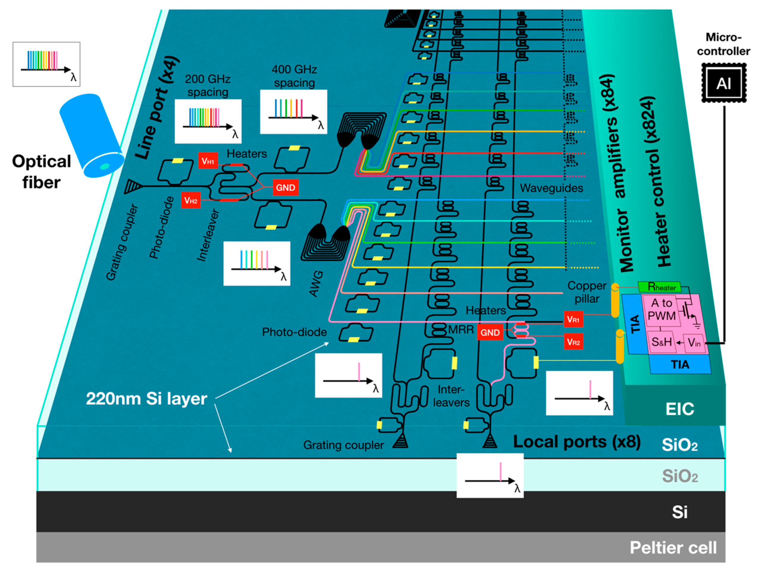
This novel integrated silicon photonic switch comes with more than a thousand optical components, each controlled by a dedicated electronic circuit, over less than 30 mm
2 chip area [
10]. The device has been achieved by flip-chip bonding the complementary metal-oxide-semiconductor (CMOS) photonic layer with the electronic chip realized in the BCD8sP technology [
11]. In particular, the photonic layer is based on a silicon-on-insulator (SOI) substrate with 2 µm buried oxide featuring a 220 nm thick silicon device layer (see
Figure 1). Feature sizes down to 120 nm have been obtained through 193 nm lithography. The CMOS fabrication flow has allowed for different photonic components on chip, such as Ge P-I-N photo-diodes, grating couplers, micro-ring resonators (MRRs), arrayed waveguide gratings (AWGs), and interleavers. Tuning capabilities are enabled by thermal heaters placed above the critical components—MRRs and interleavers [
12,
13]. The hybrid (analog-digital) control of the thermal heaters is shown in
Figure 1 (right), where an analog input voltage (Vin) is stored in a sample–and–hold (S–and–H) circuit [
14]. This allows for setting the heating power with a digital pulse-width modulation (PWM) to minimize the circuit’s power dissipation. The digital heater control works at a 1.2 GHz clock frequency in the electronic integrated circuit (EIC) [
10]. We used a 7-bit PWM resolution with a PWM frequency of 7.58 MHz, which resulted in a 128 × 128 digital voltage grid for every switching element on the chip. 3D integration of electronics on photonics has been obtained through an Al–Cu interconnection via and Cu micro-pillars [
15].
The IRIS architecture drives 48 optical channels, 200 GHz-spaced in the C-band, in 4 different directions, through 12 add/drop ports [
11]. A fully packaged prototype has been completed and tested at 25 Gbps into the operational environment, with 12 wavelengths, 4 directions, and 8 add/drop ports [
15]. The system has been optically accessed through the V-groove assembled fiber array, vertically coupled to the input/output single polarization grating couplers. The electronic control of the switch fabrics, combined with an intelligent management plane implemented on a microcontroller, enabled a complete system reconfiguration in microseconds [
14].
Compared to conventional ROADMs, which use free space optics 1xN wavelength selective switches for the optical line switching, the IRIS switch has the competitive advantage of a more than one order of magnitude lower cost (a few hundred euros) and an overall 60 times smaller device volume (few cm
3). This device can also play a key role into data centers, due to its capability to manage a large throughput in a single chip with a low power consumption. In fact, today’s major challenges in data centers are related to the topology and scalability issues [
16]. On the one hand, the typical rigid architecture, based on cascaded switches of limited bandwidth, requires an arbitration stage, which, in turn, contributes to the switching latency. On the other hand, the distribution of huge amounts of power and the complexity of cooling, limit the scalability of the infrastructures. Exploiting the embedded photonics approach, IRIS acted on both sides. The flat all-to-all (NxN) topology supports the contention-free interconnection at full throughput. The reconfigurable architecture adapts to the workload with ease, for a higher efficiency. This last point is the focus of this paper, which details the optimization methods used to initialize/reconfigure the whole IRIS chip, and the performance figures, before and after the optimization.
This paper is structured as follows. In
Section 2, we detailed the architecture of the optical switch used for our tests.
Section 3 describes the optimization method exploited to automatically initialize/reconfigure all optical elements on the optical switch. In particular,
Section 3.1 describes the core optimization engine,
Section 3.2 presents the convergence and degeneration criteria, and
Section 3.3 deals with probabilistic restarts set to avoid faults during the initialization. In
Section 4, we benchmark the optimization method, both on a ring resonator and on an interleaver.
Section 5 reports the overall performances achieved during the switch operation. Finally,
Section 6 gives the conclusions.
2. Optical Switch Architecture
The IRIS switch has a cross-bar topology, which is the most appropriate switch fabric for a multi-port switch, where the loss values of the switching elements in both the off- and on-state must be as low as possible [
17]. In
Figure 1 (left), a comb of 12 WDM channels (200 GHz spacing) reaches one of the four fiber-pigtailed input ports of the chip. At the input port, the optical signal is coupled into the photonic chip, through a single polarization grating coupler (SPGC). A multi-wavelength waveguide leads the signal to a de-interleaving stage (interleavers), which separates the channels into odd and even wavelengths (spacing relaxed to 400 GHz) [
18]. Then, the two subsets of wavelengths move toward two 1 × 6 AWGs, which take the single optical channels apart into dedicated waveguides [
19]. After the de-multiplexing stage, we have the switching matrix, where the double MRR-based switching nodes placed at the waveguide crossings can be trimmed, to drop the signal from each line. In fact, each MRR of the system comes with a dedicated metallic heater, which can be independently biased to shift the MRR resonance by the thermo-optic effect [
20,
21]. By design, all MRRs are not resonating with the wavelengths carried by the line waveguides (off-state). However, when a specific bias is applied to the heaters of a switching node, it comes in resonance (on-state) and drops the signal from the line waveguide. Thermal crosstalk is negligible. Simulations and experimental results show that, for an MRR in the off state, the thermal crosstalk from adjacent MRRs move the resonance by less than 16 GHz [
11]. Integrated photo-diodes placed after each stage, allow for an optimization based on optical feedback. We will describe the optimization method used to find the proper bias values for the two MRRs of a switching node, to drop a wanted wavelength in the next section. Moreover, at the end of
Section 5, we will address how to tackle the case of some MRRs that happened to be partially aligned, even though they should be in the off-state by design.
The switching matrix has a total of 4 × 12 rows and 8 × 2 columns. Each row is dedicated to a single wavelength, as it is depicted in the figure, using different colors. Each column collects the optical signals possibly dropped by the switching nodes and re-combines them (through an interleaver) to one output fiber. Focusing on the path highlighted in light pink, the demultiplexed signal travels into a row, until it gets to a column crossing where the two MRRs are tuned in resonance (second switch node in
Figure 1). There, the signal is dropped toward the corresponding output port. If the MRRs are not in resonance with the wavelength carried by the row, the optical signal passes through (as it happens for the other switch nodes in the figure).
The 1572 switching node heaters in the IRIS chip are controlled by an electronic chip that is bonded in a 3D fashion on the photonic one (on the right in
Figure 1). This makes it easy to access each single heater through copper pillars from the top. As for the MRRs, the interleaves arms can be thermally affected, as well. The interleavers are based on an unbalanced Mach–Zehnder interferometer (MZI) design [
22]. Each MZI branch has a dedicated heater on top, which can be independently operated. This makes it possible to cope with the production inaccuracy, which prevent the interleaves to work properly, as they have been designed. The next section describes the automatic method implemented to optimize the interleaver spectral response. Moreover, the IRIS chip is provided for a Peltier cell, which allows shifting the temperature of the whole systems. This can be used to counteract overall fabrication errors (e.g., variations in the SOI thickness [
23]), shifting the transfer function of each photonic component on the chip in a rigid way.
Note that the IRIS chip can operate in two modes—either to drop WDM channels from the line ports to the local ports, or to add the WDM channels from the local ports to the line ports. Therefore, by simply inverting the direction of the optical flows, using the local ports as inputs and the line ports as outputs, the device works in an add mode. We can achieve a ROADM by combining two IRIS devices in a sequence, such as the horizontal waveguides of one switching matrix are connected to the horizontal waveguides of a second switching matrix. One device has to be used as the add stage, and the other as the drop stage.
On the other hand, we can achieve the all-to-all (NxN) switch topology, by combining two IRIS devices in parallel, such as the local ports of the first IRIS device (used in drop mode) are connected to the local ports of the second IRIS device (used in add mode). By doing so, the wavelengths dropped at the local port of the first device are added to the second one, via the corresponding local port. Therefore, any wavelength coming in from any input line port of the first device, can be sent to any output line port of the second device.
3. Optimization Method
This section describes the optimization engine we had setup to enable the automatic initialization/reconfiguration of the active elements on the IRIS chip, i.e., switching nodes and interleavers. The core of the engine was a heuristic/stochastic algorithm, which saved us from a brute force search for the best bias configuration, to apply to the heaters of each photonic element to retrieve the wanted output transfer function.
For design reasons (due to the positioning of the integrated photo-diodes), we needed to align the resonance of each single switching node and trim each interleaver, separately. At the first alignment of the IRIS chip, namely initialization, the optimal bias configurations found were stored into a look-up-table (LUT). During operation, the LUT could be accessed to set the switching matrix into a particular routing configuration.
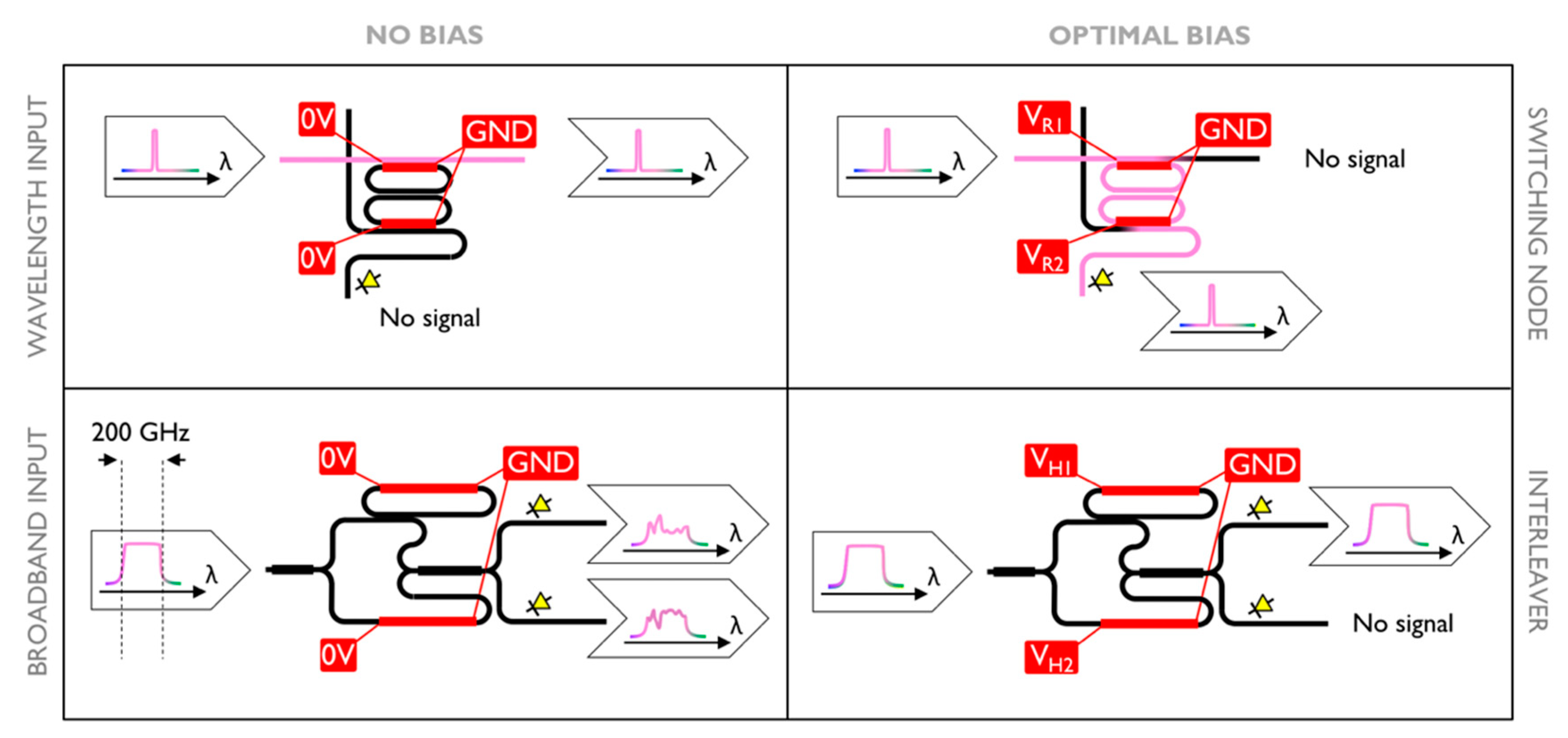
For aligning the switching nodes, the single wavelengths (from a tunable laser) were injected into the straight waveguides of the switching matrix. If no bias was applied to the MRR’s heaters, the wavelengths pass through the crossings without being dropped (with no bias, the switching nodes are in an off-state). When we launched the initialization routine, the optimization engine (one switching node at a time) searched for the heating configuration which maximized the optical signal dropped toward the local port (top panels of
Figure 2). The optimization relied on the feedback from the photo-diodes placed at the columns switching matrix, right above the interleaves. The double-ring-based node shared the same transfer function of a second-order filter. Still, it kept a single local maximum within the phase space of all possible heating configurations of the switching node. This design has been chosen to allow a 35 dB channel isolation, while keeping a channel 3 dB-bandwidth of 50 GHz [
13].
The interleavers have to be initialized as well. A schematic of the interleaving stage, before and after the optimization, is shown in the bottom panels of
Figure 2. The MZI interleavers are very sensitive to the fabrication errors and need a dedicated trimming to allow the optical signal properly entering the cross-bar matrix [
24]. In this case, the optical source (tunable laser) was injected at the interleaver input and was swept over the wavelength, within an interval of 200 GHz, i.e., one channel width. The optimization engine was fed back by the optical signal from one of the photo-diodes at the MZI output, integrated over a wavelength sweep. By doing so, we assured that the transfer function to optimize coincides with the channel shape of the interleaver, and thus, we could get to a local maximum (best channel shape, i.e., flat top response) by tuning the heaters on the MZI branches. Once we optimized the interleaver response for one output, as the two interleaver outputs were complementary, we had also optimized the response for the other output. In fact, Figure 6 demonstrates that this approach allowed to properly retrieve the wanted interleaver behavior, i.e., splitting the input optical signal into even and odd channels. Even if our optimization routine focused on a limited range of 200 GHz width, this was sufficient to optimize the routing of all the other channels, alternatively toward one or the other interleaver output (as shown in
Figure 1 for the interleaver after the input line port).
Therefore, we can exploit the same core algorithm to initialize both the switching nodes and the interleavers.
Since the dependence of the optical response of both the MRRs and the interleavers on the bias applied to the thermal heaters is not a linear, our case needed a non-linear optimization methods [
25]. The algorithms for non-linear numerical optimization could be divided in two main classes—the gradient-based methods and the direct search methods [
26]. Gradient-based algorithms use information coming from the first derivative (gradient) and the second derivative (Hessian) to find a local maximum of the target function. In absence of constraints, the Newton optimization method is the most suitable one. On the contrary, for constrained optimizations, we can either apply the sequential quadratic programming method, the extended Lagrange method, or the non-linear internal point method [
27].
However, in our case the target function was non-linear and non-differentiable, and so direct-search approaches were the most appropriate ones. In contrast to the optimization techniques that require the derivative of the objective target to determine a search direction, a direct-search method relies solely on the value of the target function on a set of points.
Direct-search methods include the Nelder-Mead (NM), the simulated annealing, and the whole class of the evolutionary algorithms [
27]. Most of these methods use the greedy criterion to make their decisions. Under the greedy criterion, a step is taken if and only if it increases the value of the target function. Although the greedy decision process converges fairly fast, it runs the risk of becoming trapped in a local minimum.
The NM method [
28], is the most popular among the unconstrained direct methods for local optimization problems. Its widespread use is due to its rapid initial convergence [
29]. This method computes and compares the target function at the
n + 1 vertices of a nondegenerate simplex (a
n-dimensional polytype of nonzero volume that is the convex hull of its
n + 1 vertices), where
n is the number of design variables. The algorithm at each iteration removes the vertex with the worst (minimum) value of the target function and replaces it with another point with a better (higher) value. The new point is obtained by reflecting, expanding, or contracting the simplex along the line, which joins the worst vertex with the centroid of the remaining vertices. If a better point cannot be found in this way, the algorithm retains only the vertex with the best value of the target function, and the simplex is shrunk by pushing all other vertices toward that value. The algorithm runs as long as the simplex converges into a local optimum. Of course, the local optimum met depends on how the starting vertices of simplex is chosen.
In the literature, we find only few examples of methods that automatically tune in resonance the high-order MRR-based filters [
30]. Mak et al. addressed this optimization problem by combining the NM with the coordinate descent method (algorithm that belongs to the class of the derivative-free optimization methods), to obtain an enhanced convergence efficiency.
Instead, we have decided to apply another version of the NM method, namely the Globalized Bounded Nelder–Mead (GBNM) method. The GBNM accounts for variable bounds and is particularly robust against stagnation of the convergence solution, into local attraction basins of the target function [
31,
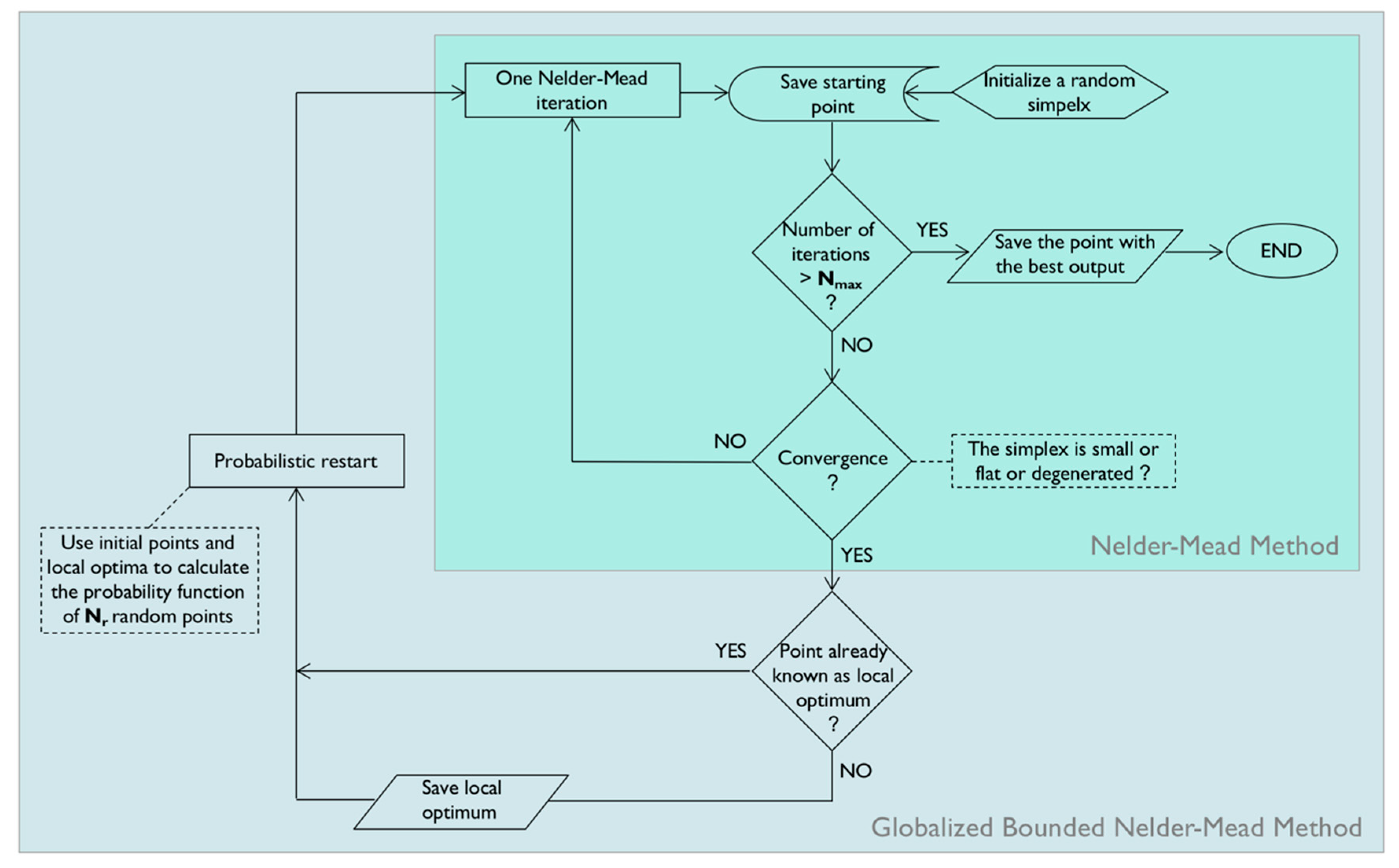
32]. In fact, it combines a local optimizer, the pure NM search, a global optimizer, to random restarts of the local optimizer. To be more effective, the random restarts are triggered by a probability function, which keeps in memory the past local searches and pushes the new searches in domain regions where no solutions have yet been found. In the following, we describe how the NM algorithm work as a numeric optimization technique. Then, we discuss the convergence criteria, degeneration conditions, and probabilistic restarts.
3.1. 2D Nelder–Mead for Maximization
Our optimization problem had 2 design variables, as only 2 heaters could be operated independently. Therefore, the simplex is a triangle, having
n = 2 + 1 = 3 vertices. Let
x =
(xi, xj) be one point of the search domain (
i,j specify the 2 dimensions of the problem), and
f(x) be the target function to maximize. At the beginning, the NM algorithm samples three points:
xk, with
k = 1, 2, 3 (the vertices of a triangle, where each vertex has two coordinates, i.e., the two biases to apply to the heaters of a switching node or of an interleaver). Then, f is evaluated at each point, returning
zk =
f(xk). The obtained values are then reordered so that
z1 ≥
z2 ≥
z3. Consequently, the sampled points (the vertices of the starting triangle in the search domain) are referred to as:
where
a =
(ai, aj) is the vertex with the best (higher) value of the target function,
b =
(bi, bj) is the vertex with neither the best nor the worst value of the target function, and
c =
(ci, cj) is the vertex with the lower value of the target function. Then the NM algorithm sets:
Then, the NM goes through the steps described in
Table 1 to find a new triangle to analyze in the next iteration.
In our optimization problem, the design variables have upper and lower constraints (i.e., from 0 to the maximum bias applicable to the heaters). Thus, we need to set a constraint box on the variables, via projection [
25]. Projection of variables can be achieved by forcing:
where
i,j represent the 2 dimensions of the search domain. When a new point is sampled by an NM iteration and one or both of its coordinates fall out of the bonds, the new point is pushed back into the constraint box. This operation guarantees the optimal solution to lie in a feasible point, in terms of heating.
3.2. Convergence and Degeneration Criteria
Each NM iteration leads to a new set of evaluation points, with the aim of converging to a “small enough” triangle with “close enough” vertices. How much “enough” accounts for is defined by the problem-dependent and user-defined values
ε1 and
ε2, both positive. The NM algorithm is said to converge if:
where
l and
u stand for lower and upper bound and the factor 10
−9 is added to prevent the ratio being meaningless if
f(a) = 0.
For computational reasons, during a NM search the simplex could collapse into a subspace of the search domain, i.e., the triangle degenerates to a segment or to a single point. This happens if one of the two following conditions is satisfied:
where
ε1 and
ε2 are small positive constants.
3.3. Probabilistic Restarts
To avoid the optimal solution from being trapped into a local attraction basin of the target function, we could execute multiple NM searches in sequence and choose the best output among the convergence points. More efficiently, the GBNM method keeps the past convergence pathways in memory and pushes new local searches far from the already sampled points of the search domain. To do so, the GBNM bases on a probability density function, which is computed at each restart.
The probability of having already sampled a point
x is:
where
N is the number of already sampled points [
31]. In the previous equation,
pg is the normal bi-dimensional probability density function, defined as:
where
and
are the coordinates of one of the already sampled points and:
where we set
α = 0.01 to make sure that the standard deviations
σi,j from the Gaussian mean cover 10% of the domain If the optimization problem has a bounded domain
Ω, we need to introduce bounded probability as:
Now, the probability density of having not sampled a point
x before is
where
xh is the domain point with the highest value of
ρ(x). This way,
xh has zero probability of having not been sampled before.
In most implementations, the GBNM does not go for a precise maximization of
Φ(x) within the search domain. This is because of the computational effort needed to accomplish this task. Instead,
Nr points are randomly pulled at each restart, and the one with the highest value of
Φ is selected as the starting point for the next NM search. The flow-chart of
Figure 3 shows how the GBNM algorithm links the probabilistic restarts to a pure NM search.
In our implementation of the GBNM method, the maximum number of restarts is not fixed, as the cost of each single local search is a priori unknown. Instead, we set a limit in the total NM iterations, so that, if a local search is taking too long, it is terminated after a while. Moreover, we compute the probability function only over the local convergence points and not over all of the already sampled points. In fact, this last option is memory- and time-consuming and shows degraded performances. Of course, the probability of having found the global optimum increases with the number of probabilistic restarts.
In the following section, we will detail the choice of the algorithm parameters, as they have been used for aligning the photonic components on the IRIS chip.
4. Algorithm Training and Benchmark
In practice, the target function we needed for optimization was the optical signal at the output of the switching nodes and the interleavers (as sketched in
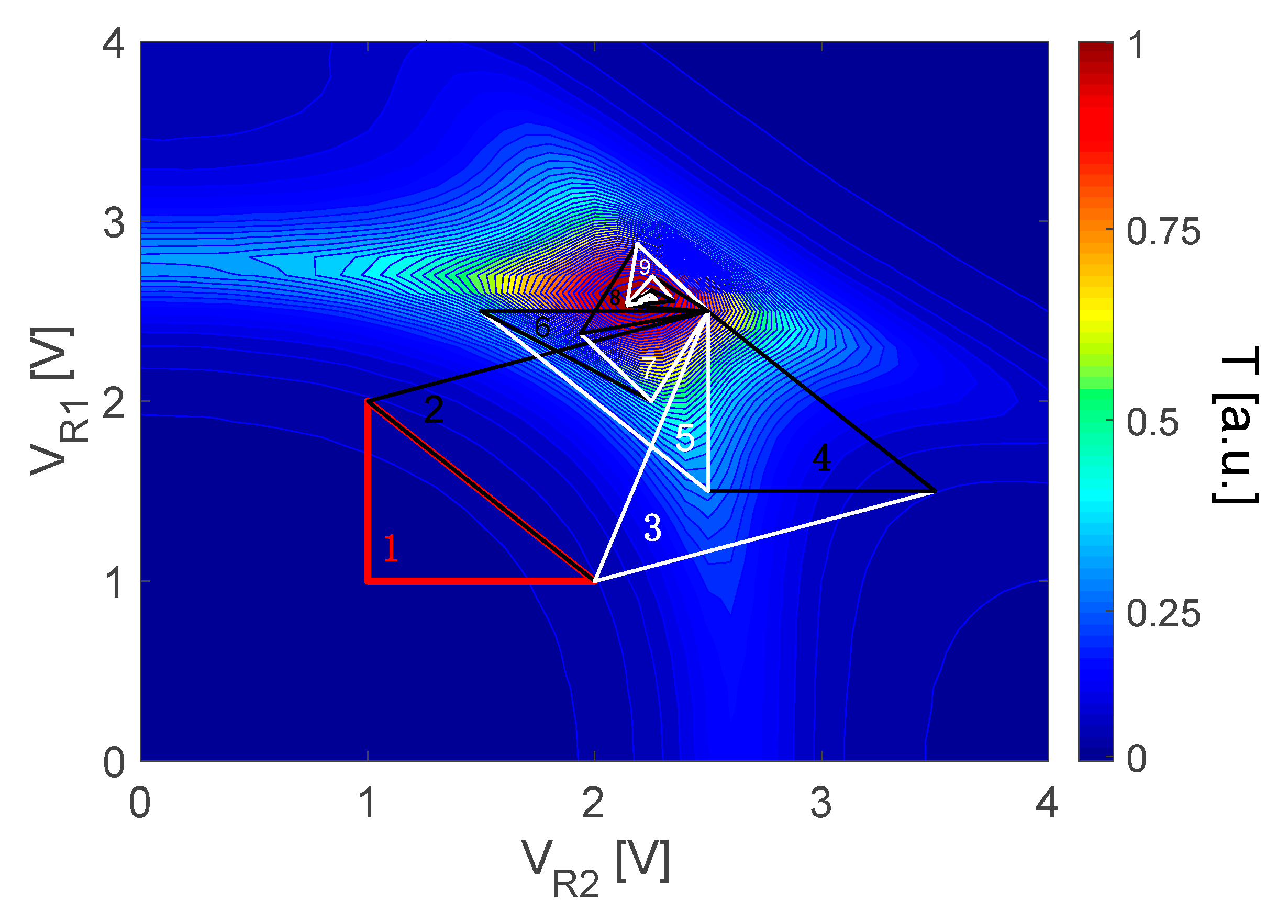
Figure 2). As an example,
Figure 4 shows the steps performed in a local NM search, to align one switching node. The contour plot in the background has been obtained by collecting the signal (T) dropped by the switching node at each point of the search domain (i.e., for all of the bias combinations applicable to the MRR heaters). Above the contour, a series of simplexes (triangles) is superimposed, which represent the evolution of the NM optimization. The starting triangle is shown in red, while alternating black and white triangles follow from the different actions toward convergence, namely reflection, expansion, contraction, and shrinkage.
We could infer the influence that the heaters in the single switching node had on each other, by noting that the contour plot was not symmetric with respect to the line connecting the domain points [4,0] and [0,4]. In fact, the upper and the rightmost tails of the surface were stretched toward the plot axes. In any case, this effect did not prevent the global maximum to be clearly distinguished by the optimization algorithm. During our tests, we also confirmed that the discretization of the search domain due to the 7-bit PWM heater control was dense enough to allow the precise tracking of the local optima, without the need to tighten the convergence/degeneration criteria.
It was clear that the target function had a single local maximum and that the NM search converged to it in a few steps. In our implementation, the starting point could be selected by the user so that we could push the first NM search in the nearby region where the maximum was expected to be.
Earlier, to launch a new NM search, the GBNM algorithm pulled
Nr points within the search domain and chose the one with the highest probability of having not been evaluated before as the next starting point. The GBNM exited when it reached a preset number of cycles,
Nmax.
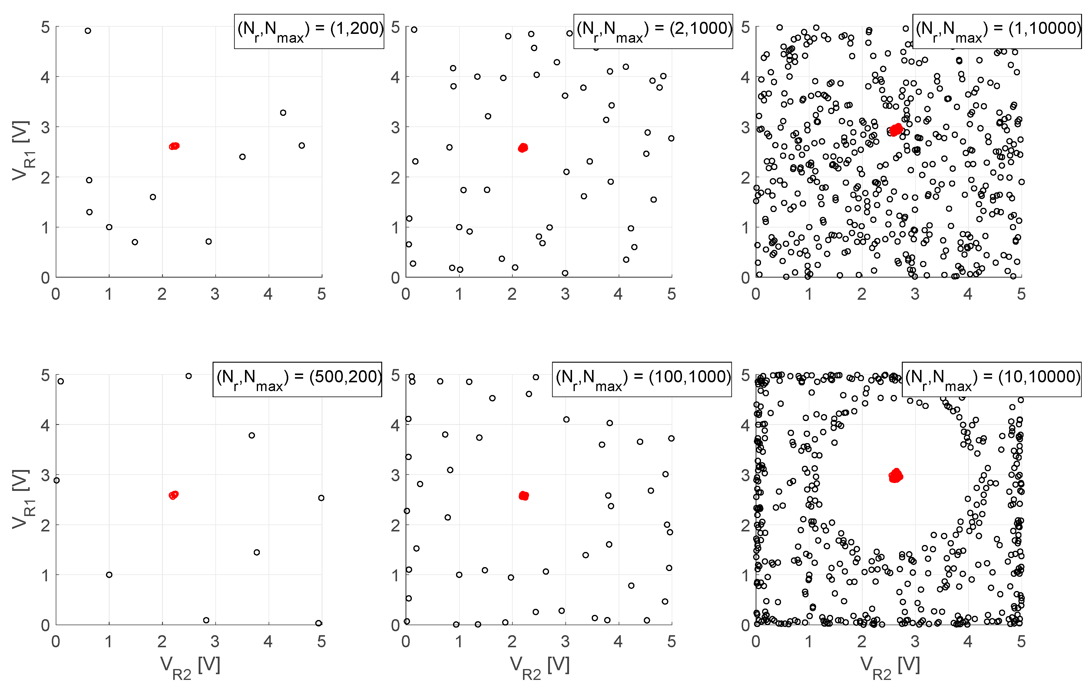
Figure 5 compares the performance of the GBNM method for several combinations of
Nr and
Nmax, when we tried to optimize a double MRR-based node. The blue circles represent the starting points of the subsequent NM searches, while the red circles represent the convergence points (local optima).
By comparing the upper two plots of
Figure 5 we can appreciate how
Nr affected the restarts when
Nmax was kept constant. If
Nr was 1, the re-initialization was completely random because no selection of the best point could be operated when the pool contained a single point (
Figure 5 (top left)). If
Nr was large (i.e., 500), the starting points come to lie on a lattice (
Figure 5 (bottom left)), as this was the geometric layout that minimized the probability density
Φ(x). So,
Nr should be chosen in such a way to reach a compromise between a random and a grid arrangement. However, it was not crucial to find the best value of
Nr for our target function, according to the outcomes showed in
Figure 5 (middle panels). In fact, these two conditions were pretty similar and we could ensure a sufficiently broad search within the domain, as well as a limited computational cost of the GBNM algorithm, if we chose
Nr ∈ [5;10].
Focusing on
Nmax, it was interesting to see what happened when it was increased to 10,000 (
Figure 5 (right panels)). With
Nr = 10, the points near a local maximum had almost no chance to be selected as the new starting points. This made the GBNM method really efficient when the target function had multiple local optima. Indeed, it pushed the restarts far from the already known attraction basins.
We obtained a similar scenario also for the interleaver, if we considered the one channel width (200 GHz) integrated optical signal at one output as the target function to optimize. Indeed, the interleaver transfer function demonstrated a local maximum when a flat top channel shape was recovered (see
Figure 2, bottom panels). In this particular condition, the photo-diode had its maximum read-out because all the optical signal injected at the interleaver input was tied to one of the interleaver output channels.
For the purpose of automatically aligning the whole IRIS chip, we implemented the GBNM optimization in a NI LabView routine, which drove a tunable diode laser Tunics BT as the source and exploited the on-chip integrated Ge photo-diodes as the feedback monitors. At each step, the routine set a different couple of bias values to the heaters of one photonic component, and followed the instruction of the optimization algorithm. Once the global optimum was determined, the routine moved to the next photonic components to align, and so on.
Of course, the duration of a single GBNM search depended on both Nr and Nmax. The higher these values were, the higher was the reliability of the global optimum and, consequentially, the higher the time taken by the optimization search. With Nr = 2 and Nmax = 150, the optimization search recovered the wanted passband of an MRR-based switching node (repeatedly) in less than 5 s. For an interleaver, the same process took almost 10 times more. This was because, at each evaluation of the target function, the routine had to sweep the tunable laser on one channel width (200 GHz) and to integrate the photo-diode read-out signal over the channel bandwidth.
To align the whole IRIS switching matrix and accomplish the LUT (for 12 interleavers and 384 switching nodes), the routine took about 12 h. This process could be significantly shortened by increasing the communication speed between the chip and the microcontroller ATxmega128A1U (currently @ 9600 bps). However, once the LUT was completed, it could be accessed at any time, allowing the complete reconfiguration/restoration of the IRIS chip in the microsecond regime.
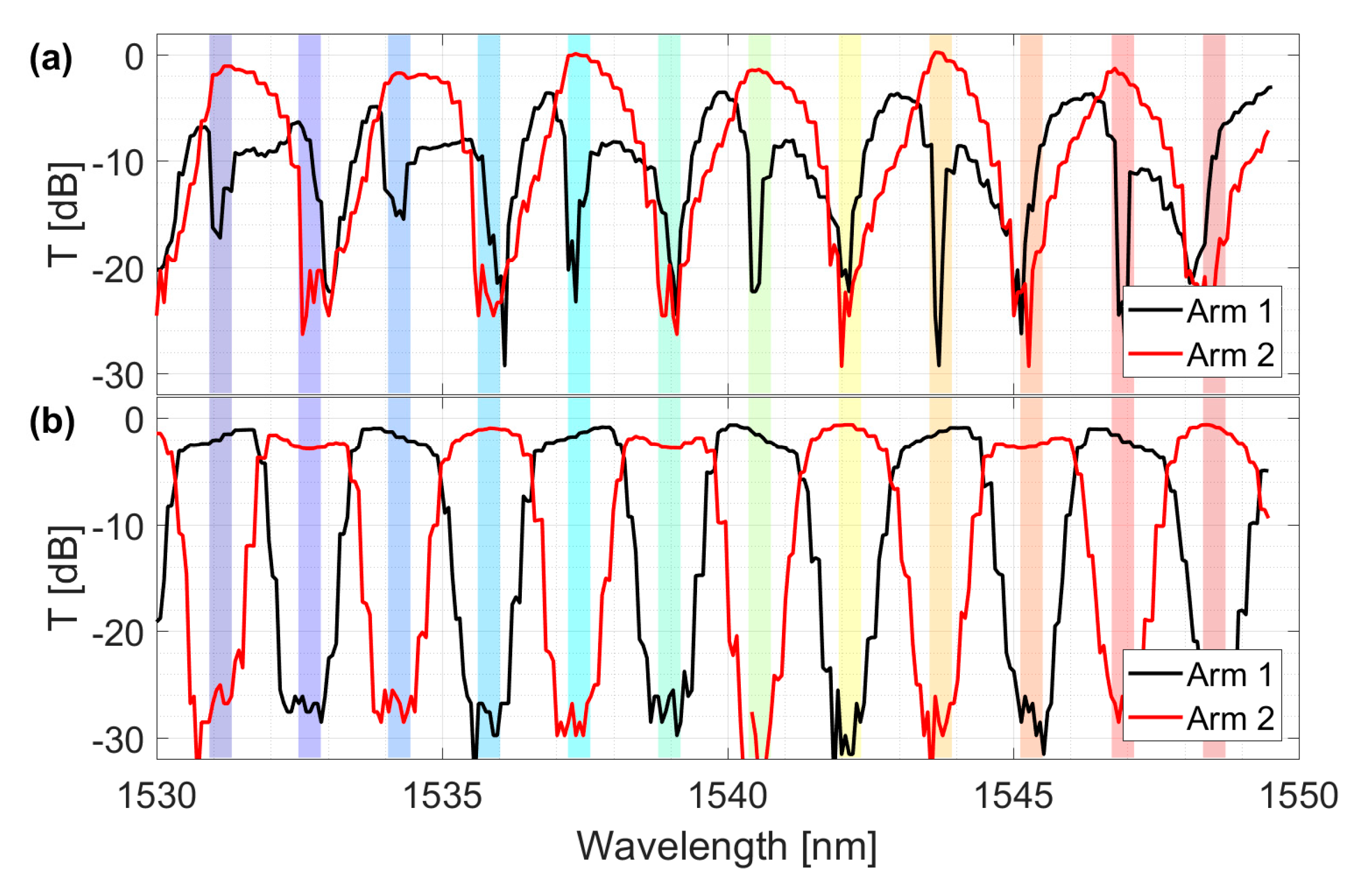
Figure 6 demonstrates the effect of the optimization algorithm on one interleaver. Specifically,
Figure 6a shows the transmission spectrum on the two arms of the interleaver in the as-received chip (before alignment). The colored slots in the picture represent the 12 ITU channels to which the IRIS device had to be aligned (between 193.6 THz and 195.8 THz with 200 GHz channel spacing). Due to the inaccuracies introduced by the fabrication process, the interleaver did not split the input signal into even and odd channels. However, once the optimal bias configuration for the heaters of the interleaver was found, the output spectrum was the one shown in
Figure 6b. Notice that the transmission spectrum was flattened within the channels slots and the insertion losses were reduced to 1 dB after the alignment.
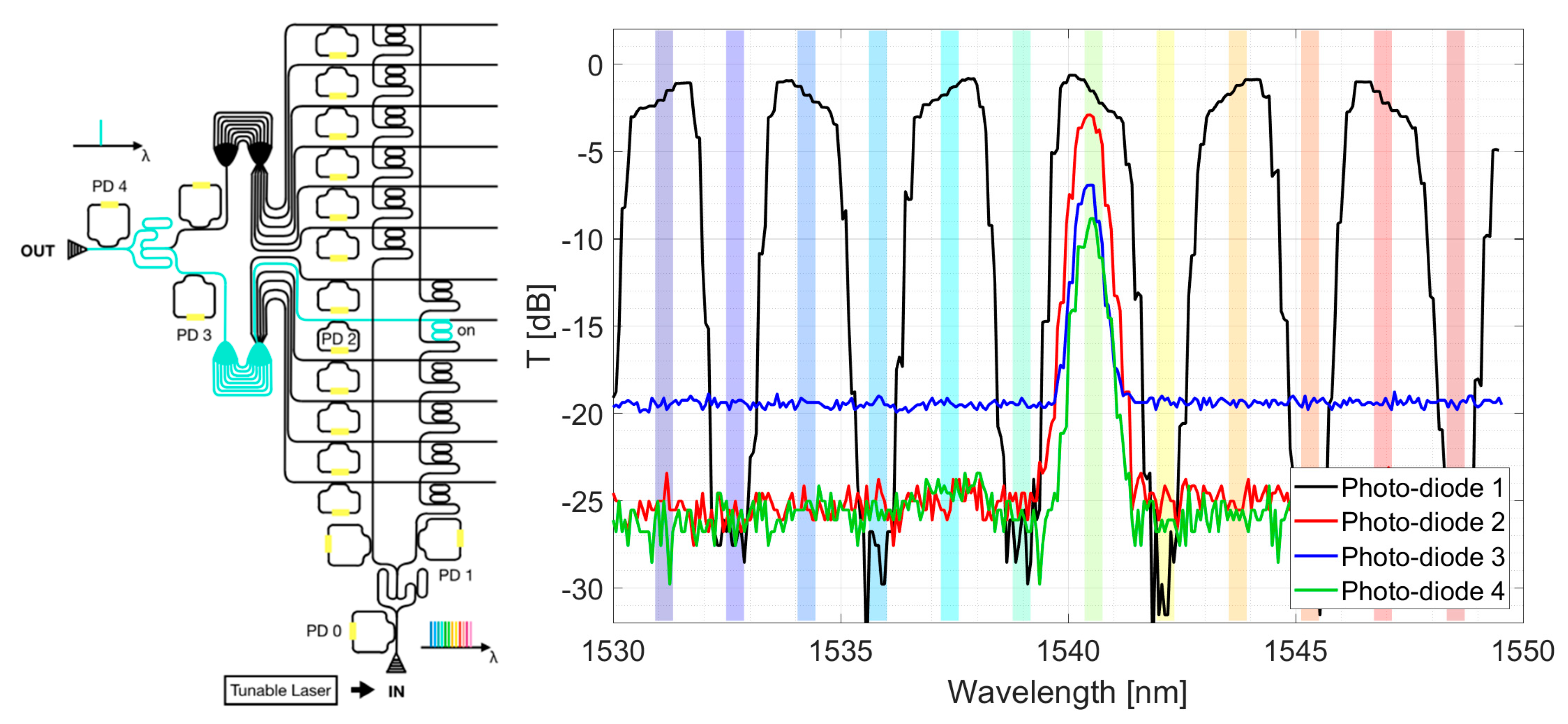
5. Overall Performances of the IRIS Device
Figure 7 reports the performances measured by the internal photo-diodes after each photonic stage of the IRIS chip. In this case we showed the device operating in the add mode, i.e., the input signal was injected from the local port to be added to one line port, as depicted in the left panel the figure. A tunable laser was used as input light source. The photonic components along the pathway were aligned according to the proposed optimization routine. The curves were normalized to the optical signal collected by the photo-diode, after the input grating coupler (PD 0 in the schematics on the left). As a first step, the light passed through the interleaver. The black curve represented the transmission spectrum at one of the two output arms (PD 1). Notice that the multispectral signal in the input was de-interleaved into the single odd channels. The red curve was acquired after the switching node which was turned to the on-state (PD 2). The MRR-based node accounted for 2 ÷ 3 dB optical losses. The blue curve showed how the AWG affected the transmission, reducing the optical power by another 3 dB (PD 3). The effect of fabrication inaccuracies on AWGs and the possible ways to correct them could be found in [
19,
33]. Finally, the green curve was collected after the second interleaver, just before the output grating coupler (PD 4).
Let us note that these measurements were acquired with a single channel being injected into the chip. When more channels were simultaneously launched at the local ports, additional inter-channel interference could arise. This crosstalk analysis has been used to fix the isolation requirements of the optical components during the chip design [
11]. Experiments in a fully aligned optical switch showed zero power penalties in the presence of 1, 2, or 3 interferences, with respect to the single channel transmission BER curve [
15].
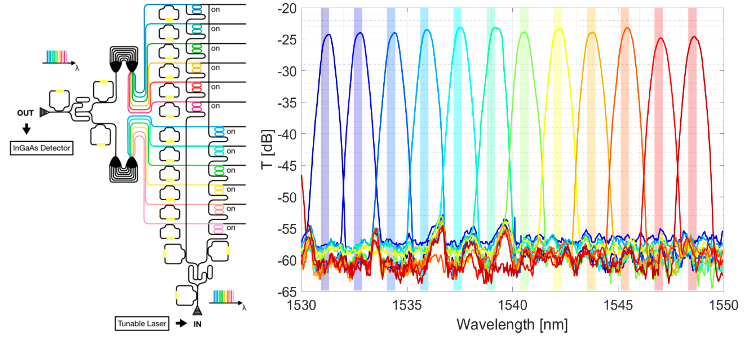
Figure 8 showed the overall fiber-to-fiber performances of the IRIS switch. Here the experimental setup consisted of a tunable laser source as input and an InGaAs photodetector fiber-coupled to the output grating coupler (sketched on the left of the figure) as the output monitor. In the figure, the 12 optical channels, which had been acquired one at a time, are superimposed. The optical signal at the InGaAs detector was normalized to the signal from the tunable laser. The IRIS chip demonstrated total insertion losses of 23.8 ± 0.5 dB. These losses come partially from the optical propagation within the device (about 9 ÷ 10 dB, as is clear from
Figure 7, green curve). The total length of the connection waveguides varied from about 1.2 cm (in the case of the shortest path) to almost 2 cm (in the case of the longest path). The rest was due to the coupling (almost 7 dB per grating coupler). It is worth noting that the far-field envelop effects were negligible, as shown in
Figure 8.
For the purpose of scalability, insertion losses had to be decreased. First, one could reduce the losses by improving the alignment of the fiber arrays with the grating couplers. In fact, fabrication errors had caused twice as large losses per grating, with respect to the design. Second, one can introduce active components by heterogeneous integration, such as optical amplifiers, in order to compensate the on-chip device losses. A more detailed discussion on this issue is given in [
15].
Focusing on the channel isolation, i.e., the difference between the intensity of the optical signal within the colored slots and the plateau of spurious signal out of the channels, we got a value of 30.1 ± 0.8 dB.
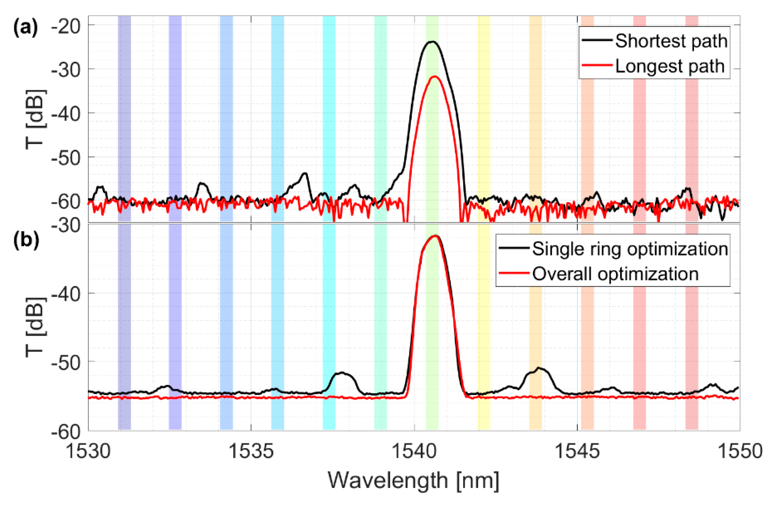
The figures reported in
Figure 8 relate to the shortest optical path on chip (the input local port and the output line port were the closest to each other). Clearly, the performances were worsened when the pathway on chip was longer. The reason was because the optical signal had to propagate along longer pieces of waveguide and go through many more crossings. This, in turn, led to higher losses. By comparing the transmission spectra of the shortest and the longest optical path on the IRIS chip (
Figure 9a), we realized an increase of 7.6 dB in the losses for the same wavelength channel. In fact, insertion losses rose up to 31.4 ± 0.2 dB, in the red curve. However, we could assign most of the loss increase to the presence of 48 additional crossings along the longest path (not to the propagation losses within the waveguides). This was consistent with the preliminary characterization of the IRIS building blocks, where we measured about 0.16 dB optical losses per single crossing [
11].
Still in
Figure 9a, we can see some side peaks rising form the noise plateau (especially in the black curve). This was due to some MRRs along the optical path which happened to be partially aligned, although all of the switching nodes should have been in the off-state by design, when not biased. This was because of inaccuracies introduced during the fabrication process. We could easily solve this issue by misaligning all of the switching nodes of the IRIS matrix in a preliminary step, before putting the device into operation. Of course this task could be addressed by exploiting the same optimization method discussed in the previous section. In fact, we could simply turn the search into a minimization problem, by looking at lowering the optical signal in the through port of the switching nodes. An example of such an operation is shown in
Figure 9b, where a better channel isolation was retrieved after the misalignment of all the switching node but the one in the on-state (red curve). Further measurements demonstrated that similar optimization performances could be achieved in all the other 11 wavelength channels. Clearly, this affected the energy budget needed to switch one wavelength channel, as more electrical power was used to keep the other switching nodes misaligned (about 20 mW per node).
6. Conclusions
This work detailed the theoretical grounds of the GBNM algorithm, and its practical use to align/restore integrated optical components as MRR switching nodes and interleavers. This optimization method dramatically reduced the steps to get the best out of devices where the spectral response depended on two or more independently tunable parameters. With the GBNM, it was not necessary to perform as many analyses as needed for an evolutionary algorithm to converge. Indeed, the global search bases on multiple local restarts of the NM method and could be terminated at will. This ensured a high probability to locate the global optimum of the target function within the search domain. In fact, it reduced the possible errors by averaging the local searches. Moreover, it represented the strategies to avoid stagnation or entrapment of the searches into degeneracy basins, through oriented/constrained search restarts.
Our implementation of the GBNM has proven to be ready for massive optimization tasks, as it allowed the failure-free alignment of all active elements within the IRIS switch. The optimization engine has been exploited in a double-edged way—on one side maximizing the performances of each single optical component, on the other side, minimizing the spurious effects introduced by the fabrication process on the other. In addition, this method could be easily extended to tunable optical circuits with an arbitrary number of input parameters (for example multi MRR switching nodes).
In the end, the optimization method proposed here could enable an efficient optical switch, as it provided an automatic light-path setup and its full reconfigurability/restoration on the fly, without the need of any external intervention.


