Abstract
This paper demonstrates a design, fabrication and performance evaluation of a frequency selective 60-GHz flexible metasurface in order to facilitate an unobstructed, secure, and low-loss high-frequency signal propagation. The high-attenuation 60 GHz millimeter-wave (MMW) band is selected for the design of a broadband metasurface. The symmetric metasurface unit-cell structure comprises of an assembly of a circular metallic ring embedded with a square-shaped ring. The screen printing process is deployed to perform fabrication of the metasurface on flexible films by means of highly-conductive nanoparticle copper pastes. Electromagnetic (EM) characteristics of the proposed structure are examined by using the quasi-optic bench testing facility in order to validate its potential contribution in the high data-rate communication links. The proposed ultra-thin and flexible metasurface can be integrated on walls and windows as wallpaper to enhance the wireless signal propagation in highly-dense indoor scenarios.
1. Introduction
In the past decades, metamaterials and metasurfaces have gathered an incredible consideration due to their unprecedented potency of tuning the electromagnetic (EM) characteristics and to achieve such EM properties not easily feasible in nature [1]. Metamaterials are three-dimensional assemblies of repeated patterns of multiple elements designed at scales that are smaller than the wavelengths of the design frequency range [2,3,4]. These structures are developed from composite materials such as metals or plastics, however, their behavior is different from the conventional materials due to the newly designed geometry. Metasurfaces, on the other hand, are two-dimensional artificial materials with precise geometry, size and orientation which enable smart properties to manipulate EM waves by restricting, absorbing, or bending the waves that cannot be achieved from the traditional materials [5,6,7]. For instance, metasurfaces are deployed as frequency selective surfaces (FSSs) to offer either band-pass or band-stop shielding [8,9]. Metasurfaces possess a planar structure with a thickness much smaller than the wavelength of incident light and allow full control over the phase, amplitude, and polarization of the EM-wave beams [10]. Metasurface has produced spectacular optical effects through which it can guide the light along an arbitrary direction, and can cause negative refraction, optical mirages to cloaking, super/hyper-lensing etc. [11,12,13,14,15]. With exceptional wave-steering capability, the metasurfaces designed for acoustic applications are capable to establish the distinctive features of realizing an abnormal reflection, demonstrated by the Snell’s law and ultrathin planar lenses [16]. These remarkable properties of metasurfaces have established profound research interest in the development of high-frequency metasurfaces for future wireless applications with preferably conformal construction to enhance the ease of integration.
The frequency response of the metasurface depends on the current distribution on the unit-cell, as the current density on the FSS is influenced by the shape of the designed unit-cell [17]. FSSs are usually designed as periodic arrays of metallic structures, such as conventional patches, loops, dipole, crosses and fractals printed on dielectric substrates, or perforated apertures on thin conductive sheets, deployed to filter out incident plane waves at certain bandwidth [17,18]. The EM characteristics of a metasurface are entirely dependent on the type of metallic geometry, size, substrate type as well as the inter-cell spacing [19]. Structural modifications can enhance the performance to a considerable extent, for instance, a high-impedance metasurface can realize electrically thin EM absorbers with better bandwidth and absorption for the TM polarization by means of metallic vias to connect patches with the ground plane [20]. It has also been investigated that the loop structures offer more angular stability than the solid metallic patches due to lesser deviation in resonant frequency, generally for TM-polarized incident plane waves [21]. In addition, circular ring metasurface can provide stability to incidence wave angles and polarizations, with lower coupling between the elements [22]. The advantages of such loop-based unit-cell structures have encouraged this research to come up with a new design combining circular and square loops in the proposed geometry of the metasurface.
In comparison with the metamaterial, metasurface can conveniently avoid the fabrication complexities involved in the synthesis of the 3D-structures and can be easily manufactured on a large scale by using conventional planar technologies. However, the performance of metasurfaces can be further enhanced by the design of novel elements/unit-cells as well as the precise and low-cost fabrication methods. In addition, the flexibility and conformity of such structures are anticipated as essential features to maximize the feasibility of integrating the wireless technology in numerous non-planar surfaces for the compact, robust, and reliable user experience [23,24]. Due to the challenges involved in the large scale fabrication of the metasurfaces based on the flexible substrates or films, several advanced techniques, such as additive and subtractive lithographic processes and various nano-printing methods have been proposed [25,26]. Among the fast and high-resolution printing techniques for bulk fabrication, screen printing is anticipated as a feasible choice due to the simplicity of the process, time-efficiency and reduced wastage, cost-effectiveness and reasonable accuracy [26].
The MMW spectrum has gathered huge research interest in moving toward the development of an ultra-fast infrastructure, with the potential to support a large number of applications and services for future networks [27]. Realization of such a massive migration from low-frequency bands to MMWs is a huge task and needs more intense efforts at different research forums to propose efficient MMW based devices and components. A high-attenuation 60 GHz band has been projected as well-suited to establish secure and high-speed point-to-point communication links for short-distance indoor networks [28]. This paper has proposed the flexible printed metasurface to be integrated into the indoor scenarios, such as walls and windows, in order to enhance the signal strength for the 60-GHz band. For a cost-effective and fast approach with reasonable accuracy, screen printing is exploited here due to its capability of bulk fabrication, making it a smart selection for EM surfaces with large surface area [23,29]. The designed metasurface is characterized to validate a broadband performance by deploying the testing setup incorporating a quasi-optic test bench.
2. Materials and Methods
The physical implementation of the MMW metasurface on flexible materials is highly critical due to the optimization required for the parameters which determine the precision, robustness and reliability of the printed pattern. Type of a flexible substrate is important in radio-frequency (RF) circuit design and the selection is usually made among the available options based on the electrical, mechanical and thermal properties of the material. Recyclable and eco-friendly plastics, polyesters, polyimides and polymers have been widely investigated in developing flexible electronics for the wearable and conformal applications. For instance, polypropylene, a thermoplastic polymer which can withstand temperatures up to 160 °C, has been used with aluminum metallization to implement an RFID antenna [30], and MMW metasurface constituting split-ring and complementary split-ring resonators [31]. Moreover, liquid crystal polymer (LCP) is highly anticipated for MMW flexible antennas and RF circuitries due to low dielectric loss, moisture repellent, chemicals resistant, and can handle up to 300 °C [32]. In addition, polyethylene terephthalate (PET) by DuPont (Melinex ST504) is a crystal-clear, high-gloss, heat-stabilized and widely available thermoplastic polymer film from the polyester family. Due to its cost-effectiveness and eco-friendly recycling qualities, it is produced in bulks and has been consumed in disposable packaging and in the manufacture of several resins [33]. Melinex films with varying composition, permittivity and thickness are commercially available and have been deployed in many reported flexible printed circuits [34,35]. In order to perform patterning by means of a suitable ink or paste, the Melinex sheet is preheated at one side to improve adhesion. Also, polyimide film produced by DuPont (Kapton) is suitable for flexible devices because of outstanding features of flexibility, mechanical, chemical and thermal stability as well as constitutes an inert and hydrophobic surface [36]. In this research, Melinex and Kapton films have been selected as substrates for the metasurface design and printing due to their high-performance attributes.
A fabrication technique capable to produce precise small-scale dimensions and ensures high-speed and low-cost manufacturing is desired to produce large panels of metasurface which can be deployed as wallpapers. Several state-of-the-art processes have been considered in this regard. For instance, flexible films with a copper/aluminum cladded metal surface can be deployed for laser prototyping, though a costly solution as it requires an expensive laser milling machine [37]. Inkjet printing is an additive fabrication technique which involves a controlled layer-by-layer deposition of ink for precise patterning on flexible films by an inkjet printer [38]. The number of nozzles used for printing determines the speed of the process, and this can be extended to a reel-to-reel process for mass production. Flexography is a roll-to-roll process, comparatively faster than inkjet printing though has a limited resolution [39]. Photolithography deposits a pattern on a substrate by means of light masking and involves a layer-by-layer growth sequence, which requires a sophisticated clean-room [40]. The screen printing process, on the other hand, avoids the expensive facilities of laser prototyping, inkjet printing or a clean-room, and ensures a reasonable pattern accuracy and time-efficiency [41]. The screen stencil is typically a fine mesh constructed from silk or steel and is partially covered with an ink-blocking coating to define the print pattern. The pattern on the screen allows the conductive paste to be transferred on the substrate. In this research work, the screen printing process has been chosen for metasurface realization due to the advantages of low equipment cost, reasonable printing quality and high conductivity. Several types of conductive inks and paste are commercially available which can be deployed for this process. Nanoparticle copper paste from Intrinsiq UK was selected in this work. Figure 1 demonstrates the basic illustration of a screen printing process.
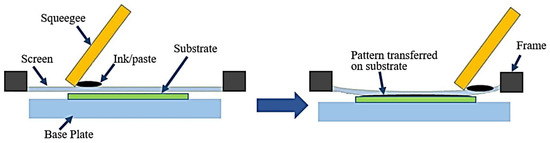
Figure 1.
An illustration of a conventional screen printing process.
2.1. Design and Modelling of 60-GHz Metasurface in Simulation
A metasurface is designed and developed by the addition of a thin interface with an array of subwavelength-scaled resonators to dramatically alter the reflection and transmission coefficients due to the resultant change in boundary conditions and excitation of effective currents on the surface. The subwavelength resonator size becomes critical to implement at higher frequencies and generally requires sophisticated micro-fabrication techniques. It is important to design such geometries which can ensure stability in performance against the fabrication tolerances that can cause minor variations in the size and radiating length. This concern has been fully considered in this work while designing a resonator geometry, and a stable structure comprised of a circular loop embedded with the square loop has been introduced. The proposed design offers more angular stability and lesser deviation in the resonant frequency than the I–shaped resonator reported in Reference [23]. The design and modelling of the metasurface, as well as the parametric analysis of the design variables, is carried out by using the Computer Simulation Technology (CST) Microwave Studio software established on the Finite Integral Techniques (FIT) for EM computations.
Two flexible substrate materials with excellent flexibility and durability, i.e., Melinex (thickness, h1 = 125 μm, dielectric constant, εr1 = 2.9, loss tangent, tanδ = 0.06) and Kapton (h2 = 75 μm, εr2 = 3.5, tanδ = 0.002), have been selected. The optimized dimensions of the metasurface unit-cell designed at 60-GHz are 2.8 mm (0.56 λo) × 2.8 mm (0.56 λo) × 0.135 mm (0.027 λo). The increased fraction value of the wavelength in the dimensions of the design in comparison with the [23] has made this design more convenient to realize without using highly complex small-scale fabrication techniques. Figure 2 shows the metasurface with a dual loop ring resonator, i.e., a circular ring embedded with a square-shaped ring, designed on a substrate film. Figure 2a shows the optimized design of the unit cell which has been subsequently fabricated and tested. The top layer consists of the array of electrically resonant dual loop metallic resonators with the optimized dimensions of the parameters as, a = 1.16 mm, b = 0.99 mm, c = 0.20 mm and d = 0.25 mm. The flexible manipulation of the EM waves at the subwavelengths is accomplished by a repeated patterning of the designed unit-cell in an infinite 2D plane to realize a metasurface, where a 5 × 5 unit-cell section is shown in Figure 2b as a periodicity representation. Simulation of a single unit-cell is performed with periodic boundary conditions and floquet ports to construct an infinite metasurface excited by a plane-wave. The infinite is positioned at z = 0 and the impinging plane wave impinges on the surface at an incidence angle θ. The surface radiates a collimated beam, which shows a waveguide-like ability of the designed medium.
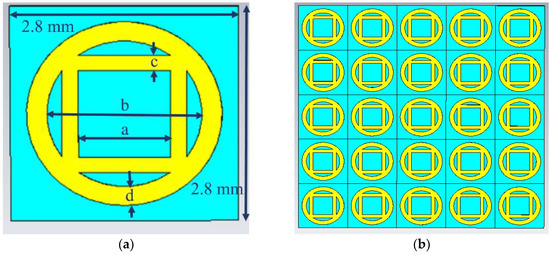
Figure 2.
The geometry of the proposed 60 GHz flexible metasurface in simulation (a) simulated unit-cell with the dimensions, (b) A 5 × 5 unit-cell segment displayed from the infinite metasurface array.
2.2. Fabrication of 60-GHz Metasurface
Several conductive inks, pastes and epoxies have been developed and reported for the screen printing of flexible electronics. Intrinsiq UK supplies multiple variants of copper-based nanoparticle pastes and ink depending on variation in the composition percentage, fluid wettability, adhesion due to bonding with the substrate surface, and conductivity which is mainly related to the concentration of the copper particles. The screen printable nanocopper-based paste CP-007 with a solid weight of ~77%, fluid viscosity of 20–35 Pa S at 25 °C, the density of ~2.6 g/mL is used for printing the metasurface. Another variant to ink CP-005 from Intrinsiq UK was used in Reference [23] with higher density and solid nanoparticle metal content. It has been observed that in this work, using a paste with lesser density, improved wettability and better ink flow has facilitated to achieve the close approximation of actual dimensions by a screen printing process, as the suggested conductive paste flows well at the edges of the mask. While in Reference [23], high density of ink was responsible for the reduced size of the realized pattern, and the shorter length shifted the resonant band to some extent towards higher frequencies. The standard screen of size 200 mm × 340 mm, comprising a fine stainless-steel mesh firmly captured within a wooden frame, with a mesh count of 325/inch and a wet print thickness of ~62 μm is used. The selected mesh count contains a standard aperture size of ~42 μm and a mesh opening ratio of ~39%. The pattern is engraved on the screen with a 12 μm thick photo emulsion coating to transfer the paste. A squeegee tilt of 45° is deployed, and a reasonable level of accuracy has been achieved.
The next step involves the curing and sintering of the printed metasurface to achieve the desired level of conductivity, which is also carried out in the manufacturing facilities of the Intrinsiq UK. The heat sintering process is recommended suitable for the conductive paste CP-007 used in this work by the manufacturers, unlike CP-005 ink from Reference [23] where laser sintering was a suitable choice. Laser sintering, though a fast and efficient method, however, involves high risks if a precise control over the intensity of the laser beam and exposure time is not carefully adopted. Heat sintering, on the other hand, has been found quite flexible and adjustable in this regard. The convection oven set at a temperature of 60 °C is used for drying, while the heat exposure time is 30–60 min. For sintering process, the temperature is increased to 180 °C for a 1-h duration, and the sample is placed in the convection oven in a reduced atmosphere of argon or nitrogen with a 3% formic acid vapor. The profilometer measurements depict that the layer thickness of the copper pattern is ~7–10 µm and the sheet resistance computed by using a 2-point probe test range from 5–7 mΩ/sq/25 µm over the entire screen-printed metasurface. These values suggest that the computed conductivity of the printed sheet is approximately 1.4 × 10⁶–3.3 × 10⁶ S/m. The screen-printed prototypes of the designed metasurface at 60 GHz are shown in Figure 3a,b on Melinex and Kapton, respectively. The adhesion of the printed patterns is examined by following the manual testing procedures, such as stretching, bending or folding over a certain curvature, as well as destructive testing by scotch tape test. These tests have confirmed the reliability and robustness of the prototypes under strain conditions as no visible cracks or damage is observed afterwards.
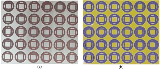
Figure 3.
Images of small segments from the extended geometries of fabricated prototypes of 60-GHz metasurface: (a) Printed prototype of Melinex, (b) Printed prototype on Kapton.
3. Results and Discussion
This section presents the results of the proposed metasurface as well as the parametric analysis of the design variables in the CST software. While the experimental testing in the setup, designed on the operating principle of placement of the metasurface sample perpendicular to the direction of radiation of the two antennas, to measure the transmission characteristics is also investigated here.
3.1. Simulated Results of the 60-GHz Metasurface
Two flexible substrates, i.e., Melinex and Kapton have been used, thus the material properties of both of the substrates have been incorporated in the simulation. The designed structure in the CST software is illuminated by a plane wave at a normal incidence angle of the inward travelling plane wave, where the polarization of the electric field is in the x-direction. Figure 4a shows the simulated S-parameter plots of the reflection (S11 and S22), and transmission coefficients (S12 and S21). The transmission is fully blocked at 60 GHz with a −41.5 dB magnitude and the complete reflection of 0.06 dB is observed. While the transmission is isolated across the metasurface, it acts like a guided medium and allows the signal to propagate along the surface. Simulated results show that a bandwidth of about 6.7 GHz (56.6–63.3 GHz) is achieved at −20 dB reference. Figure 4b shows the phase profile where the phase of transmission coefficients coincides with 0° at the designed frequency of 60 GHz along with a phase coverage of ±180°.
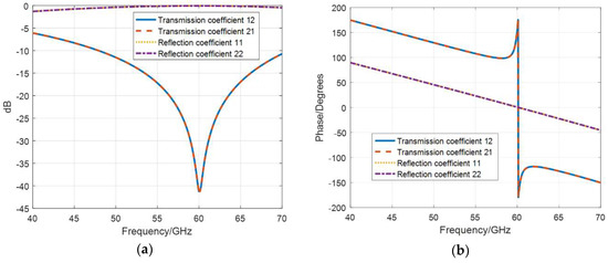
Figure 4.
Simulated plots of magnitude and phase of the 60-GHz flexible metasurface: (a) Reflection and transmission coefficients plots, (b) Phase of the reflection and transmission coefficients.
3.2. Parametric Analysis and Optimization of the Results of the 60-GHz Metasurface
In order to optimize the performance of the designed metasurface structure, it is important to examine the effect of variation of the design parameters of the unit-cell geometry on the magnitude and phase of the S-parameters. The effect of some main parameters such as dimensions of the dual loop metasurface and the angle of the incidence wave on the transmission, reflection coefficient and their phases are investigated in this analysis.
3.2.1. Angle of Incidence
To inspect the effect of the angle of the incident wave on the S-parameters results of the reflection and transmission coefficients and reflection phase of the metasurface, the numeral analysis with various angles of the incident wave is carried out for the proposed free-standing band-pass metasurface design in the CST software. Figure 5 shows the reflection phase, reflection coefficient and the transmission coefficient with the varying angles of incidence of the wave in the range of 0° to 50°. From the reflection phase plot in Figure 5a, it can be deduced that the phase is dependent on the incidence angle. This has been observed that as the incidence angle increases, the reflection phase angle also increases. The reflection coefficient and transmission coefficients from Figure 5b,c, on the other hand, show relatively lesser dependence on the variation of the scan angle of incidence at 60 GHz. Since the direction of incidence is relative to the top and bottom of the designed dual loop metasurface, it is expected that the bandpass frequency should remain stable regardless of the direction of external EM signal without any significant alteration. The reflection coefficient in the whole angle of incidence shows it is almost complete (less than −0.2 dB) while the transmission coefficients are almost blocked (~−50 dB). A wide bandwidth greater than 9 GHz at −10 dB reference is achieved that covers the 60 GHz band of interest in all the considered angle of incidence.
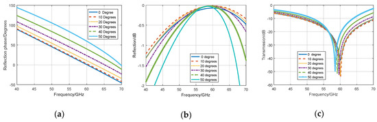
Figure 5.
Reflection phase, reflection coefficient and transmission coefficient of the dual loop metasurface at a varied angle of incidence, θ: (a) Reflection phase, (b) reflection coefficient and (c) transmission coefficient.
3.2.2. Square Loop Length, ‘a’
It has been observed from the simulation analysis that the square loop length ‘a’ of the dual loop metasurface has a significant influence on the reflection and transmission coefficients profiles with a relatively lesser effect on the reflection phase as shown in Figure 6a. As the value of ‘a’ increases, the resonant frequency shifts to the left, which indicates a decreasing magnitude of the design frequency as in Figure 6b,c. The possible explanation of this phenomenon is, the increase in the inner square size, ‘a’ has lengthened the current path of the metasurface, and thus it results in the decrease of the resonant frequency. In this case, the reflection phases are set within the range 0° to 20° for each iteration of the parametric analysis. The plots show that at the frequency of consideration, i.e., 60 GHz, as the ‘a’ increases, the reflection phase decreases, however, at ‘a’ = 1.16 mm, the reflection phase is exactly at 0°. The bandwidth remain almost constant (9 GHz) from a = 0.96 mm to a = 1.16 mm before decreasing at ‘a’ = 1.36 mm. While considering the reflection phase and the resonant frequency at 60 GHz, an optimal value of a = 1.16 mm is selected.
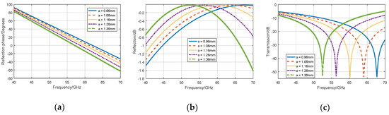
Figure 6.
Reflection phase, reflection coefficient and transmission coefficient of the dual loop metasurface at varied square loop length, ‘a’: (a) Reflection phase, (b) reflection coefficient and (c) transmission coefficient.
3.2.3. Inner Radius, ‘b’
The parametric study of the inner radius ‘b’ of the circular loop has shown a considerable variation on the transmission coefficient profile, by shifting the resonant frequency. The plots of Figure 7a–c shows that as ‘b’ increases from 0.89 mm to 1.09 mm, the design frequency decreases to this point. However, a critical change is observed at ‘b’ = 1.14 mm where the resonant frequency increases. This shows, there is a cut-off point for the inner radius to negate the trend of increasing size that results in lengthening the surface current. At ‘b’ = 0.99 mm, the resonant frequency is 60 GHz with a reflection phase of 0°, therefore, b = 0.99 mm is selected as the optimized value for the proposed unit-cell of the metasurface.
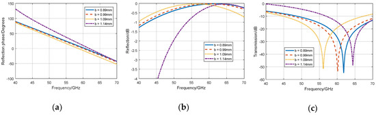
Figure 7.
Reflection phase, reflection coefficient and transmission coefficient of the dual loop metasurface at the varied inner radius, ‘b’: (a) Reflection phase, (b) reflection coefficient and (c) transmission coefficient.
3.2.4. Thickness of the Square Loop, ‘c’
The analysis presented in Figure 8 shows that the thickness of the square loop ‘c’ has more impact on the resonant frequency depicted by the transmission coefficient plot than the reflection coefficient of the dual loop metasurface. From the plots in Figure 8, it can be deduced that as ‘c‘ increases from 0.15 mm to 0.30 mm, the resonant frequency also increases, except at 0.10 mm, as shown by the transmission coefficient plot of Figure 8c. The reflection coefficient magnitudes at 60 GHz are approx. −0.2 dB at varying values of ‘c’ as shown in Figure 8b. The reflection phase falls within 3% of 0° as ‘c’ increases from 0.15 mm to 0.30 mm, except at 0.10 mm when it is about 10% as shown in Figure 8a. This may be due to the narrow space between the square loops which restricts the smooth flow of the surface current. A wide bandwidth that covers the desired frequency band if 60 GHz is observed at −20 dB reference.
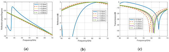
Figure 8.
Reflection phase, reflection coefficient and transmission coefficient of the dual loop metasurface at the varied thickness of the square loop, ‘c’: (a) Reflection phase, (b) reflection coefficient and (c) transmission coefficient.
3.3. Experimental Testing Setup of the 60-GHz Metasurface
In order to perform the experimental testing, a sample (metasurface under test–MUT) is placed in the path of converged radiation beams of the two horn antennas. The free-space quasi-optic bench is deployed for the testing purposes, which is comprised of a pair of corrugated horns with a bandwidth of 50–75 GHz acting as transmitter and receiver, two pairs of reflecting mirrors one of which is designed to create a full reflection at an angle of 90°, and a sample holder which allows for the transmission of radiation beams through the sample. The experimental setup is presented in Figure 9, where the sample placement is shown in Figure 9a and the complete quasi-optic bench is depicted in Figure 9b. The horn antennas are screw-fitted to their respective frequency multiplier modules, which are connected to the ports of the vector network analyzer (VNA). The highly directional beams from the corrugated horn antennas are focused toward the sample through a specified path directed by reflecting mirrors for the measurements of transmission characteristics. The inner-most pair of mirrors are designed to collimate the radiating beams with a high-quality focus over a broadband range. The sample is oriented perpendicular to the direction of antenna beams, and a VNA is used for the measurements of phase and magnitude of the reflection and transmission characteristics.
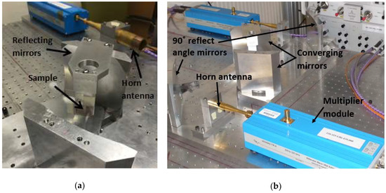
Figure 9.
Testing of the designed metasurface by using the quasi-optic bench for the measurement of transmission at 60 GHz (a) sample mounted in the test bench, (b) complete quasi-optic bench.
3.4. Measured Results of the 60-GHz Metasurface
Figure 10a,b presents the measured results of the designed metasurface screen-printed on Melinex and Kapton flexible films, respectively. Fabrication accuracy, as well as the precision of the results, are determined by the reproducibility of results, thus multiple samples have been taken randomly from a long printed pattern. Three samples taken from various locations and variable distances apart from each of the screen-printed metasurface film have been tested in the quasi-optic bench to validate the reliability and precision of the measurements. The plots show that both of the metasurfaces cover 60 GHz band and the achieved bandwidth is above 5 GHz while considering a strict estimation of −20 dB as a reference level. Though it is also observed that the resonant dip shows a slight offset towards the lower frequency range. This frequency shift towards the left side is mainly due to fabrication tolerances or dilation of substrate films due to heat exposure while heat sintering. However, the overall performance of the metasurface is not affected by this resonant shift as the operating bandwidth fully covers the 60 GHz band.
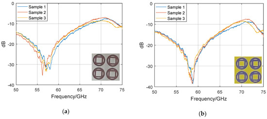
Figure 10.
Measured results of the transmission coefficient of the 60-GHz metasurface: (a) Melinex based metasurface, (b) Kapton based metasurface.
As the reliable performance can be ensured on the bandwidth by taking -10 dB reference, in this case, it has been observed that the range of 50–67 GHz has been covered in all the measured results of both of the metasurfaces. The measured bandwidth of 17 GHz has been accomplished from the proposed design which is significantly wider than that reported in [23] (i.e., 10 GHz bandwidth in the range 57.5–67.5 GHz), and more evenly extended on the left and right side of the resonant frequency of 60 GHz. Also, the proposed bandwidth of multiple samples remains conserved as the measured plots converge. The results have shown that when the antenna beams are oriented perpendicular to the designed FSS metasurface, the transmission is blocked in the bandwidth of 50–67 GHz, which implies that the signal propagates on the surface and this can be deployed as a low-loss wireless guiding medium. The proposed structure can be used as wallpapers on walls and windows to enhance the signal transmission for this highly attenuated 60-GHz band and allows a secure communication in the indoor environments.
4. Conclusions
This paper shows the potential utilization of flexible MMW metasurface as wallpapers or screens, in order to effectively improve signal communication and to maximize the power transmission in the indoor environments. The proposed screen-printed metasurface has been designed for the 60 GHz highly attenuated band, and its performance is evaluated by using the state-of-the-art testing facilities. The measurement of the flexible metasurface printed on Melinex and Kapton films is carried out on a quasi-optic bench, in order to validate the transmission characteristics of the simulations. The measured results depict an operating band of 60-GHz as the transmission is fully blocked perpendicular to the metasurface. This implies that the signal propagates on the surface of the designed metasurface and it acts like a waveguide medium to transfer the signal between two points with lesser loss than the wireless signal propagation. The proposed research is instrumental for conformal implements with desired flexibility to mount on irregular or non-planar surfaces.
Author Contributions
O.P.F., S.F.J. and A.A. performed conceptualization and methodology; O.P.F. carried out software and formal analysis; prototype fabrication is done by T.W. and P.R.; experimental investigation, validation, and data processing is done by S.F.J.; writing—review and editing is done by S.F.J. and O.P.F.; and the project administration, funding acquisition and supervision is done by A.A.
Funding
This research was funded by the grants 132216 AMMETEX—Advanced Materials and Metamaterial Structures for MetaTextiles, and EP/N029666/1 Enabling High-Speed Microwave and Millimetre Wave Links (MiMiWaveS).
Acknowledgments
Special thanks to Intrinsiq UK for the fabrication facilities and the Queen Mary University of London for the testing facilities.
Conflicts of Interest
The authors declare no conflict of interest.
References
- Zheludev, N.I.; Kivshar, Y.S. From metamaterials to metadevices. Nat. Mater. 2012, 11, 917–924. [Google Scholar] [CrossRef] [PubMed]
- Wang, B.; Wang, L.; Wang, G.; Huang, W.; Li, X.; Zhai, X. Theoretical investigation of broadband and wide-angle terahertz metamaterial absorber. IEEE Photonic Technol. Lett. 2014, 26, 111–114. [Google Scholar] [CrossRef]
- Turpin, J.P.; Werner, D.H.; Wolfe, D.E. Design considerations for spatially reconfigurable metamaterials. IEEE Trans. Antennas Propag. 2015, 63, 3513–3521. [Google Scholar] [CrossRef]
- Luo, Y.; Kikuta, K.; Han, Z.; Takahashi, T.; Hirose, A.; Toshiyoshi, H. An active metamaterial antenna with MEMS-modulated scanning radiation beams. IEEE Electron Device Lett. 2016, 37, 920–923. [Google Scholar] [CrossRef]
- Wong, J.P.S.; Epstein, A.; Eleftheriades, G.V. Reflectionless wide-angle refracting metasurfaces. IEEE Antennas Wirel. Propag. Lett. 2016, 15, 1293–1296. [Google Scholar] [CrossRef]
- Li, A.; Luo, Z.; Wakatsuchi, H.; Kim, S.; Sievenpiper, D.F. Nonlinear, active, and tunable metasurfaces for advanced electromagnetics applications. IEEE Access 2017, 5, 27439–27452. [Google Scholar] [CrossRef]
- Zhuang, Y.; Wang, G.; Zhang, Q.; Zhou, C. Low-scattering tri-band metasurface using combination of diffusion, absorption and cancellation. IEEE Access 2018, 6, 17306–17312. [Google Scholar] [CrossRef]
- Wang, L.B.; See, K.Y.; Zhang, J.W.; Salam, B.; Lu, A.C.W. Ultrathin and flexible screen-printed metasurfaces for EMI shielding applications. IEEE Trans. Electromagn. Compat. 2011, 53, 700–705. [Google Scholar] [CrossRef]
- Masud, M.M.; Ijaz, B.; Ullah, I.; Braaten, B. A compact dual-band EMI metasurface shield with an actively tunable polarized lower band. IEEE Trans. Electromagn. Compat. 2012, 54, 1182–1185. [Google Scholar] [CrossRef]
- Chen, H.T.; Taylor, A.J.; Yu, N. A review of metasurfaces: Physics and applications. Rep. Prog. Phys. 2016, 79, 076401. [Google Scholar] [CrossRef] [PubMed]
- Smith, D.R.; Padilla, W.J.; Vier, D.C.; Nemat-Nasser, S.C.; Schultz, S. Composite medium with simultaneously negative permeability and permittivity. Phys. Rev. Lett. 2000, 84, 4184–4187. [Google Scholar] [CrossRef] [PubMed]
- Datta, S.; Chan, C.T.; Ho, K.M.; Soukoulis, C.M. Effective dielectric constant of periodic composite structures. Phys. Rev. B 1993, 48, 14936. [Google Scholar] [CrossRef]
- Pendry, J.B.; Schurig, D.; Smith, D.R. Controlling electromagnetic fields. Science 2006, 312, 1780–1782. [Google Scholar] [CrossRef] [PubMed]
- Fang, N.; Lee, H.; Sun, C.; Zhang, X. Sub-diffraction-limited optical imaging with a silver superlens. Science 2006, 308, 534–537. [Google Scholar] [CrossRef] [PubMed]
- Chen, H.; Chan, C.T.; Sheng, P. Transformation optics and metamaterials. Nat. Mater. 2010, 9, 387–396. [Google Scholar] [CrossRef] [PubMed]
- Li, Y.; Jiang, X.; Li, R.; Liang, B.; Zou, X.; Yin, L.; Cheng, J.C. Experimental realization of full control of reflected waves with subwavelength acoustic metasurfaces. Phys. Rev. Appl. 2014, 2, 064002. [Google Scholar] [CrossRef]
- Munk, B.A. Frequency-Selective Surfaces: Theory and Design; John Wiley & Sons: New York, NY, USA, 2000. [Google Scholar]
- Da Silva, M.R.; de Lucena Nóbrega, C.; Silva, P.H.D.F.; d’Assunção, A.G. Optimal design of frequency selective surfaces with fractal motifs. IET Microw. Antennas Propag. 2014, 8, 627–631. [Google Scholar] [CrossRef]
- Panwar, R.; Lee, J.R. Progress in frequency selective surface based smart electromagnetic structures: A critical review. Aerosp. Sci. Technol. 2017, 66, 216–234. [Google Scholar] [CrossRef]
- Luukkonen, O.; Costa, F.; Simovski, C.R.; Monorchio, A.; Tretyakov, S.A. A thin electromagnetic absorber for wide incidence angles and both polarizations. IEEE Trans. Antennas Propag. 2009, 57, 3119–3125. [Google Scholar] [CrossRef]
- De Cos, M.E.; Las-Heras, F. On the advantages of loop-based unit-cell’s metallization regarding the angular stability of artificial magnetic conductors. Appl. Phys. A Mater. Sci. Process. 2015, 118, 699–708. [Google Scholar] [CrossRef]
- Huang, F.; Chiu, C.; Wu, T.; Chiou, Y. A circular-ring miniaturized-element metasurface with many good features for frequency selective shielding applications. IEEE Trans. Electromagn. Compat. 2015, 57, 365–374. [Google Scholar] [CrossRef]
- Falade, O.P.; Jilani, S.F.; Ahmed, A.Y.; Wildsmith, T.; Reip, P.; Rajab, R.Z.; Alomainy, A. Design and characterisation of a screen-printed millimetre-wave flexible metasurface using copper ink for communication applications. Flex. Print. Electron. 2018, 3, 045005. [Google Scholar] [CrossRef]
- Jilani, S.F.; Rahimian, A.; Alfadhl, Y.; Alomainy, A. Low-profile flexible frequency-reconfigurable millimetre-wave antenna for 5G applications. Flex. Print. Electron. 2018, 3, 035003. [Google Scholar] [CrossRef]
- Walia, S.; Shah, C.M.; Gutruf, P.; Nili, H.; Chowdhury, D.R.; Withayachumnankul, W.; Bhaskaran, M.; Sriram, S. Flexible metasurfaces and metamaterials: A review of materials and fabrication processes at micro- and nano-scales. Appl. Phys. Rev. 2015, 2, 011303. [Google Scholar] [CrossRef]
- Khan, S.; Lorenzelli, L.; Dahiya, R.S. Technologies for printing sensors and electronics over large flexible substrates: A review. IEEE Sens. J. 2015, 15, 3164–3185. [Google Scholar] [CrossRef]
- Rappaport, T.S.; Xing, Y.; MacCartney, G.R.; Molisch, A.F.; Mellios, E.; Zhang, J. Overview of millimeter wave communications for fifth-generation (5G) wireless networks—With a focus on propagation models. IEEE Trans. Antennas Propag. 2017, 65, 6213–6230. [Google Scholar] [CrossRef]
- Liu, P.; Renzo, M.D.; Springer, A. Line-of-sight spatial modulation for indoor mmWave communication at 60 GHz. IEEE Trans. Wirel. Commun. 2016, 15, 7373–7389. [Google Scholar] [CrossRef]
- Xiao, G.; Aflaki, P.; Lang, S.; Zhang, Z.; Tao, Y.; Py, C.; Lu, P.; Martin, C.; Change, S. Printed UHF RFID reader antennas for potential retail applications. IEEE J. Radio Freq. Identif. 2018, 2, 31–37. [Google Scholar] [CrossRef]
- De Cos, M.E.; Las-Heras, F. Polypropylene-based dual-band CPW-fed monopole antenna [Antenna applications corner]. IEEE Antennas Propag. Mag. 2013, 55, 264–273. [Google Scholar] [CrossRef]
- Aznabet, M.; Navarro-Cía, M.; Kuznetsov, S.A.; Gelfand, A.V.; Fedorinina, N.I.; Goncharov, Y.G.; Beruete, M.; Mrabet, O.E.; Sorolla, M. Polypropylene-substrate-based SRR- and CSRR-metasurfaces for submillimeter waves. Opt. Express 2008, 16, 18312–18319. [Google Scholar] [CrossRef] [PubMed]
- Jilani, S.F.; Munoz, M.O.; Abbasi, Q.H.; Alomainy, A. Millimeter-wave liquid crystal polymer based conformal antenna array for 5G applications. IEEE Antennas Wirel. Propag. Lett. 2019, 18, 84–88. [Google Scholar] [CrossRef]
- Jilani, S.F.; Alomainy, A. An inkjet-printed MMW frequency-reconfigurable antenna on a flexible PET substrate for 5G wireless systems. In Proceedings of the Loughborough Antennas & Propagation Conference (LAPC 2017), Loughborough, UK, 13–14 November 2017; pp. 1–3. [Google Scholar]
- Guo, X.; Hang, Y.; Xie, Z.; Wu, C.; Gao, L.; Liu, C. Flexible and wearable 2.45 GHz CPW-fed antenna using inkjet-printing of silver nanoparticles on PET substrate. Microw. Opt. Technol. Lett. 2017, 59, 204–208. [Google Scholar] [CrossRef]
- Jilani, S.F.; Alomainy, A. Millimeter-wave conformal antenna array for 5G wireless applications. In Proceedings of the 2017 IEEE International Symposium on Antennas and Propagation & USNC/URSI National Radio Science Meeting, San Diego, CA, USA, 9–14 July 2017; pp. 1439–1440. [Google Scholar]
- Fang, Y.; Hester, J.G.D.; Su, W.; Chow, J.H.; Sitaraman, S.K.; Tentzeris, M.M. A bio-enabled maximally mild layer-by-layer Kapton surface modification approach for the fabrication of all-inkjet-printed flexible electronic devices. Sci. Rep. 2016, 6, 39909. [Google Scholar] [CrossRef] [PubMed]
- Rabbani, M.S.; Ghafouri-Shiraz, H. Liquid crystalline polymer substrate-based THz microstrip antenna arrays for medical applications. IEEE Antennas Wirel. Propag. Lett. 2017, 16, 1533–1536. [Google Scholar] [CrossRef]
- Mashayekhi, M.; Winchester, L.; Pease, T.; Laurila, M.-M.; Mäntysalo, M.; Ogier, S.; Terés, L.; Carrabina, J. Evaluation of aerosol, superfine inkjet, and photolithography printing techniques for metallization of application specific printed electronic circuits. IEEE Trans. Electron. Devices 2016, 63, 1246–1253. [Google Scholar] [CrossRef]
- Olkkonen, J.; Lehtinen, K.; Erho, T. Flexographically printed fluidic structures in paper. Anal. Chem. 2010, 82, 10246–10250. [Google Scholar]
- Watson, D.E.; Ng, J.H.; Desmulliez, M.P.Y. Additive photolithography based process for metal patterning using chemical reduction on surface modified polyimide. In Proceedings of the 18th European Microelectronics & Packaging Conference, Brighton, UK, 12–15 September 2011; pp. 1–7. [Google Scholar]
- Eshkeiti, A.; Reddy, A.S.G.; Emamian, S.; Narakathu, B.B.; Joyce, M.; Joyce, M.; Fleming, P.D.; Bazuin, B.J. Screen printing of multilayered hybrid printed circuit boards on different substrates. IEEE Trans. Compon. Packag. Manuf. Technol. 2015, 5, 415–421. [Google Scholar] [CrossRef]
© 2019 by the authors. Licensee MDPI, Basel, Switzerland. This article is an open access article distributed under the terms and conditions of the Creative Commons Attribution (CC BY) license (http://creativecommons.org/licenses/by/4.0/).