Article

Enhanced Radiative Recombination Rate by Local Potential Fluctuation in InGaN/AlGaN Near-Ultraviolet Light-Emitting Diodes

by
Abu Bashar Mohammad Hamidul Islam
1,
Dong-Soo Shim
2,3 and
Jong-In Shim
1,2,*
1
Department of Electronics and Communication Engineering, Hanyang University ERICA, Ansan 15588, Korea
2
Department of Photonics and Nanoelectronics, Hanyang University ERICA, Ansan 15588, Korea
3
Department of Bionanotechnology, Hanyang University ERICA, Ansan 15588, Korea
*
Author to whom correspondence should be addressed.
Appl. Sci. 2019, 9(5), 871; https://doi.org/10.3390/app9050871
Submission received: 31 December 2018 / Revised: 16 February 2019 / Accepted: 25 February 2019 / Published: 28 February 2019
(This article belongs to the Special Issue Internal Quantum Efficiency of III-Nitride Light-Emitting Diodes)

Abstract

:
We investigate the differences in optoelectronic performances of InGaN/AlGaN multiple-quantum-well (MQW) near-ultraviolet light-emitting diodes by using samples with different indium compositions. Various macroscopic characterizations have been performed to show that the strain-induced piezoelectric field (FPZ), the crystal quality, and the internal quantum efficiency increase with the sample’s indium composition. This improved performance is owing to the carrier recombination at relatively defect-free indium-rich localized sites, caused by the local in-plane potential-energy fluctuation in MQWs. The potential-energy fluctuation in MQWs are considered to be originating from the combined effects of the inhomogeneous distribution of point defects, FPZ, and indium compositions.

1. Introduction

Recently, InGaN-based multiple-quantum-well (MQW) near-ultraviolet (NUV) light-emitting diodes (LEDs) have attracted great attention in many application areas [1,2,3]. These LEDs are promising candidates for various applications such as fluorescence light sources for lighting and displays, and excitation sources for resin curing, medicine, and banknote identification [1,2,3,4,5,6,7,8,9]. However, there still exist several issues concerning these NUV LEDs, such as reliability [10], which hinder market penetration and higher performance achievement for these applications.
The indium compositions of the quantum wells (QWs) in NUV LEDs are typically a few percent for wavelengths below 400 nm, which has a detrimental effect on light extraction efficiency (LEE) owing to the absorption of NUV light by the p-GaN layer [11]. The band-offset between the well and the barrier [2,3,12] is also affected. Thus, carriers overflow owing to the reduced carrier confinement in QWs, causing poor radiative recombination rates. Consequently, the device shows nonideal performances with high injection currents.
On the other hand, nitride-based epitaxial layers are usually grown on c-plane sapphire substrates. The large lattice mismatch between the epitaxial layers and the sapphire substrate causes numerous threading dislocations (in the order of 108–1012 cm−2) [1,13]. In addition, there are many point defects in epitaxial layers [14], which also reside in active QWs. These defects limit radiative recombination at low currents as the carriers have leakage paths through these defects [14,15].
However, the efficiencies of these QWs turn out to be surprisingly high despite high-density defects [13,16]. It has been suspected that such high efficiencies are caused by the localization of carriers by the potential-energy fluctuation in the QWs, which prevents the carriers from recombining nonradiatively at defects [13,16,17]. The possible reasons reported for carrier localization include alloy fluctuation with the incorporation of In [18,19,20,21], thickness variation of QWs [20,21], In–N–In chains [22], In clustering [23], crystal quality [24], In/Ga segregation [17], crystallographic defects [14,25,26,27,28], the piezoelectric field (FPZ) [21,28,29], and the combined effects of point defects and FPZ [30]. It has been widely accepted that excited carriers are spatially separated from defects owing to higher electrical potential energy at the edge of defects, which prevents carriers from diffusing into them [13,16,25,26,30]. Carriers thus radiatively recombine at the nondefective region, which increases the efficiencies of LEDs.
The efficiency decreases are due to Shockley–Read–Hall (SRH) recombination or tunneling leakage through defects at low currents, and carrier overflow initiated by saturation phenomena at high currents. The carrier overflow from the QWs can be decreased by effectively designing the barriers [2,3,12,31]. At low currents, quantum efficiency increases when the defect density in the active region becomes small. However, it is almost impossible to completely eliminate defects from the InGaN-based QWs grown on sapphire substrates. Thus, it is necessary to understand how defects influence radiative recombination and affect the optoelectronic performance of LEDs.
Therefore, in this study, we utilized NUV LED samples with different In compositions without any specially designed barrier to comprehend the increase in radiative recombination rates at low currents where defects play an important role. We found that the increase in radiative recombination rates at low currents was owing to spatial localization of carriers caused by the local potential-energy fluctuation in QWs [17,18,19,20,21,22,23,24,25,26,27,28,29] that originated from the combined effects of point defects, FPZ, and In compositions.
There has been research investigating the potential-energy fluctuation through material characterization and numerical simulations [17,18,19,20,21,22,23,24,25,26,27,28,29]. However, there still exists a lack of comprehensive research work using macroscopic characterizations to understand the potential-energy fluctuation in QWs. Therefore, in this work, we reported on the effects of local potential-energy fluctuation in InGaN/AlGaN MQWs that influence device performance by using a proposed carrier recombination model. We employed various kinds of macroscopic characterization techniques such as current-voltage (I-V), ideality factor (n), peak wavelength (λp), light output power vs. current (L-I), internal quantum efficiency (IQE), two-dimensional photoemission-microscopy (PHEMOS), electroluminescence (EL) and electroreflectance (ER) characteristics to identify the potential-energy fluctuation and assess the performance of these LEDs.

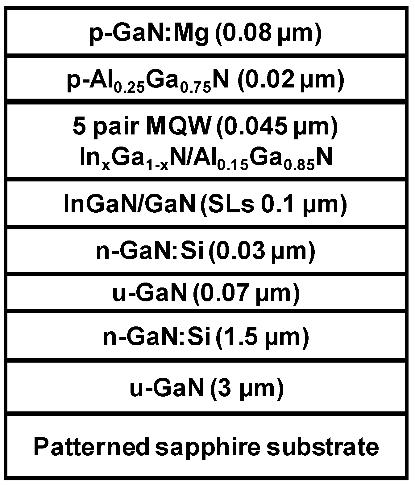
2. Samples and Experiments

The identically structured NUV LEDs were grown on a c-plane patterned sapphire substrate by using metal-organic chemical vapor deposition (MOCVD), beginning with a ∼20-nm-thick GaN layer deposited at 520 °C. After this thin layer growth, the temperature was increased to 1090 °C to grow a 3-μm-thick undoped GaN layer, a 1.5-μm-thick Si-doped n-GaN layer, a 70-nm-thick undoped GaN layer and a 30-nm-thick Si-doped n-GaN layer (n-doping = 5 × 1018 cm−3). The MQWs consisting of 3 nm-thick InxGa1–xN wells sandwiched by 5-nm-thick Al0.15Ga0.85N barriers were grown on a 100-nm-thick InGaN/GaN superlattice layer at 830 °C. Subsequently, the temperature was raised to 1000 °C to grow a 20 nm-thick Mg-doped p-Al0.25Ga0.75N electron block layer (EBL). An 80-nm-thick Mg-doped p-GaN layer (p-doping = 7.5 × 1017 cm−3) was then grown at 950 °C. These samples were subsequently annealed at 750 °C in a N2 ambient for the activation of acceptors in Mg-doped layers. Trimethylindium (TMIn), trimethylgallium (TMGa), trimethylaluminum (TMAl), and ammonia (NH3) were used as the In, Ga, Al, and N precursors, respectively. Silane (Si2H6) and bis(cyclopentadienyl)magnesium (Cp2Mg) were used as the n- and p-type dopants, respectively. Hydrogen and nitrogen were used as carrier gases. The details of the 5-QW NUV LEDs structure are shown in Figure 1.
The In compositions of samples #1, #2, #3 and #4 were estimated to be approximately 4.5%, 5.5%, 6.5%, and 7.5%, respectively. These In compositions were varied by controlling the flow rate of TMIn except sample #4 where the QW growth temperature was decreased by 10 °C from sample #3. After the epitaxial growth of NUV LED samples with different In compositions, an indium–tin–oxide (ITO) contact was evaporated onto the Mg-doped p-type GaN layer to serve as the p-electrode. A Ti/Al/Ti/Au metal contact was then deposited on the Si-doped n-GaN layer to form the n-electrode which was exposed by partial etching. The LEDs were fabricated with lateral electrodes, diced into 1000 × 1000 μm2 chips, and packaged on metal cans without epoxy for optical and electrical characteristic measurements.
Various optoelectronic characteristics measured on these samples are summarized in Table 1. For the ER spectroscopy, the probe beam was generated by using a 150-W Xe-arc lamp, which was combined with a 0.25-m dual grating monochromator (DK240). The LED was vertically illuminated by this probe beam with a wavelength resolution of 0.007 nm. For phase-sensitive detection, a lock-in amplifier (SR81) was used and the internal electric field was modulated by a function generator. A modulation voltage of 100 mVpp at 500 Hz was applied to the sample. The reflected beam from the sample was detected by a photomultiplier tube (Hamamatsu R9110).

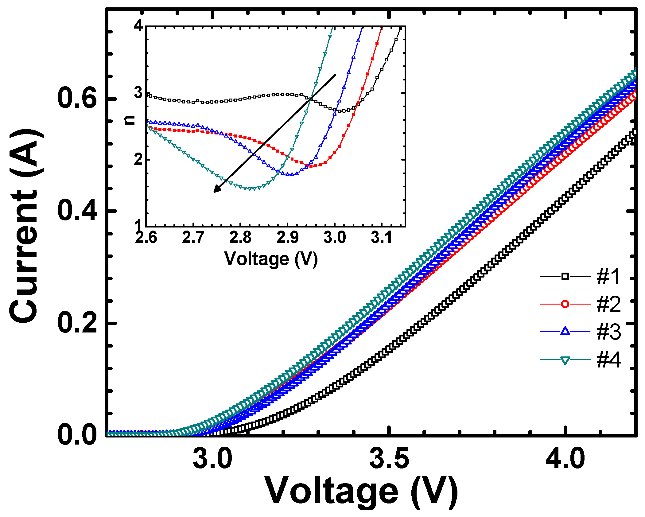
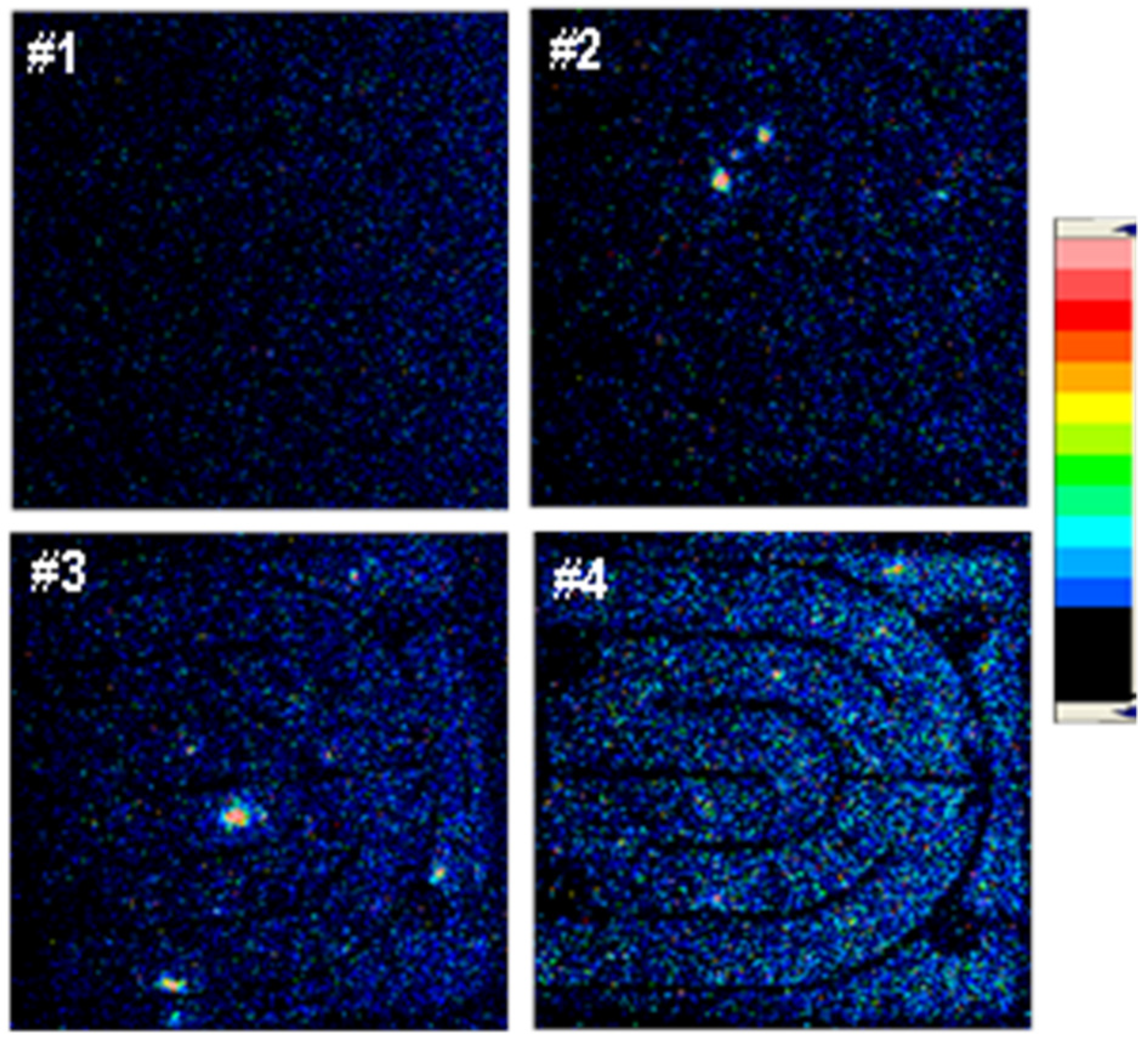
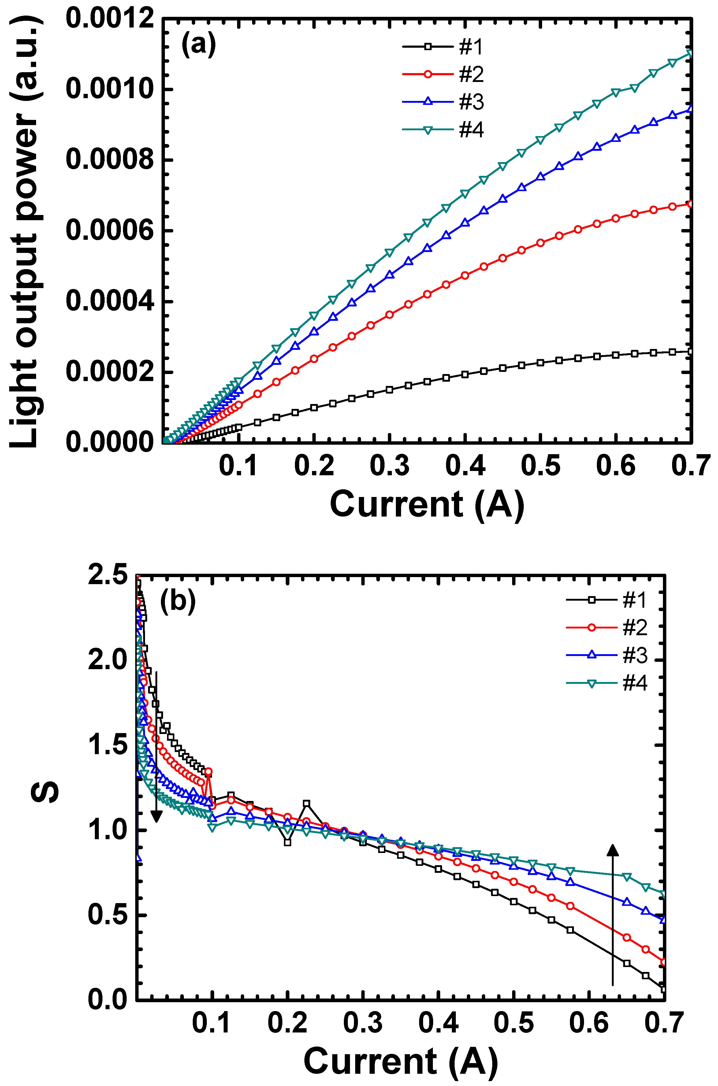
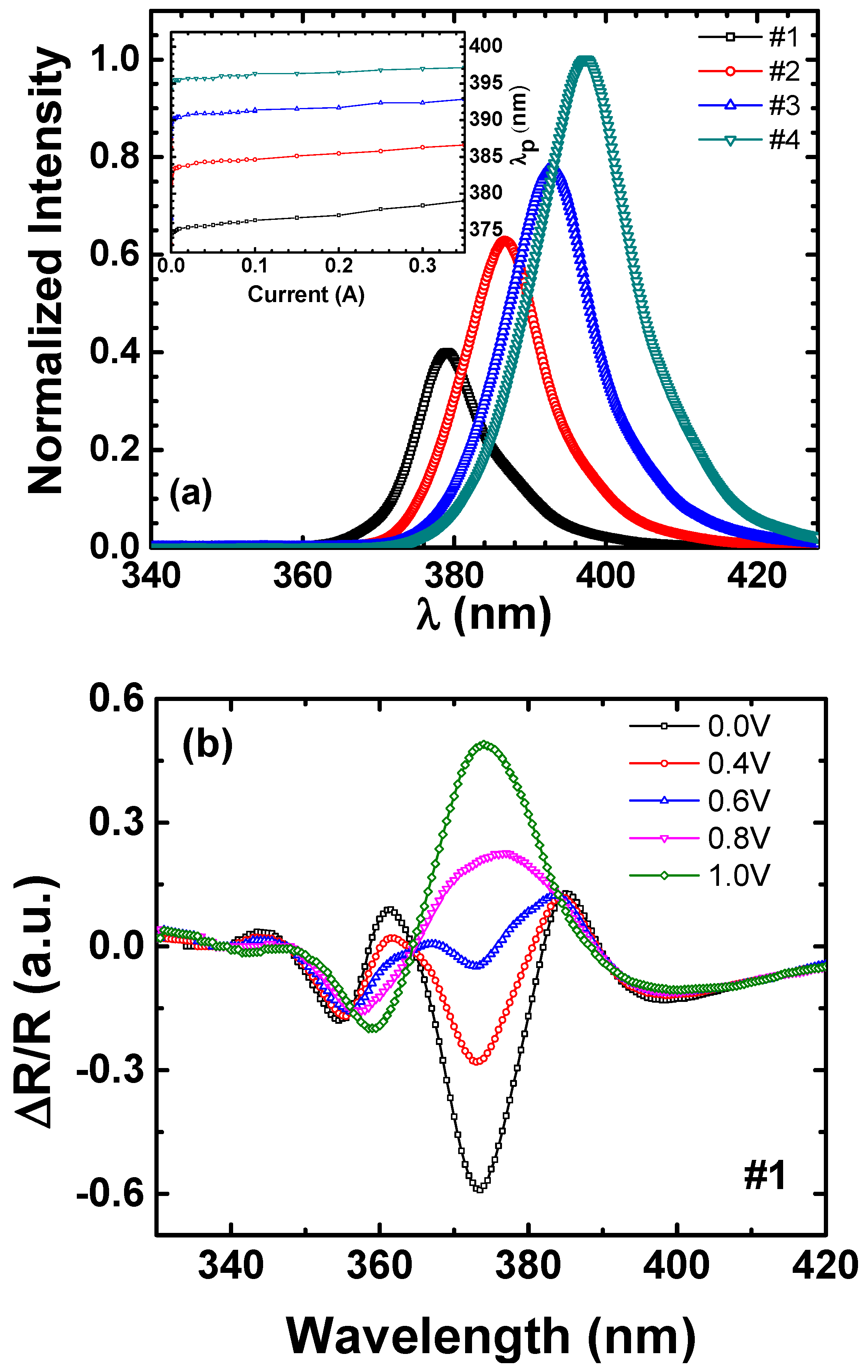
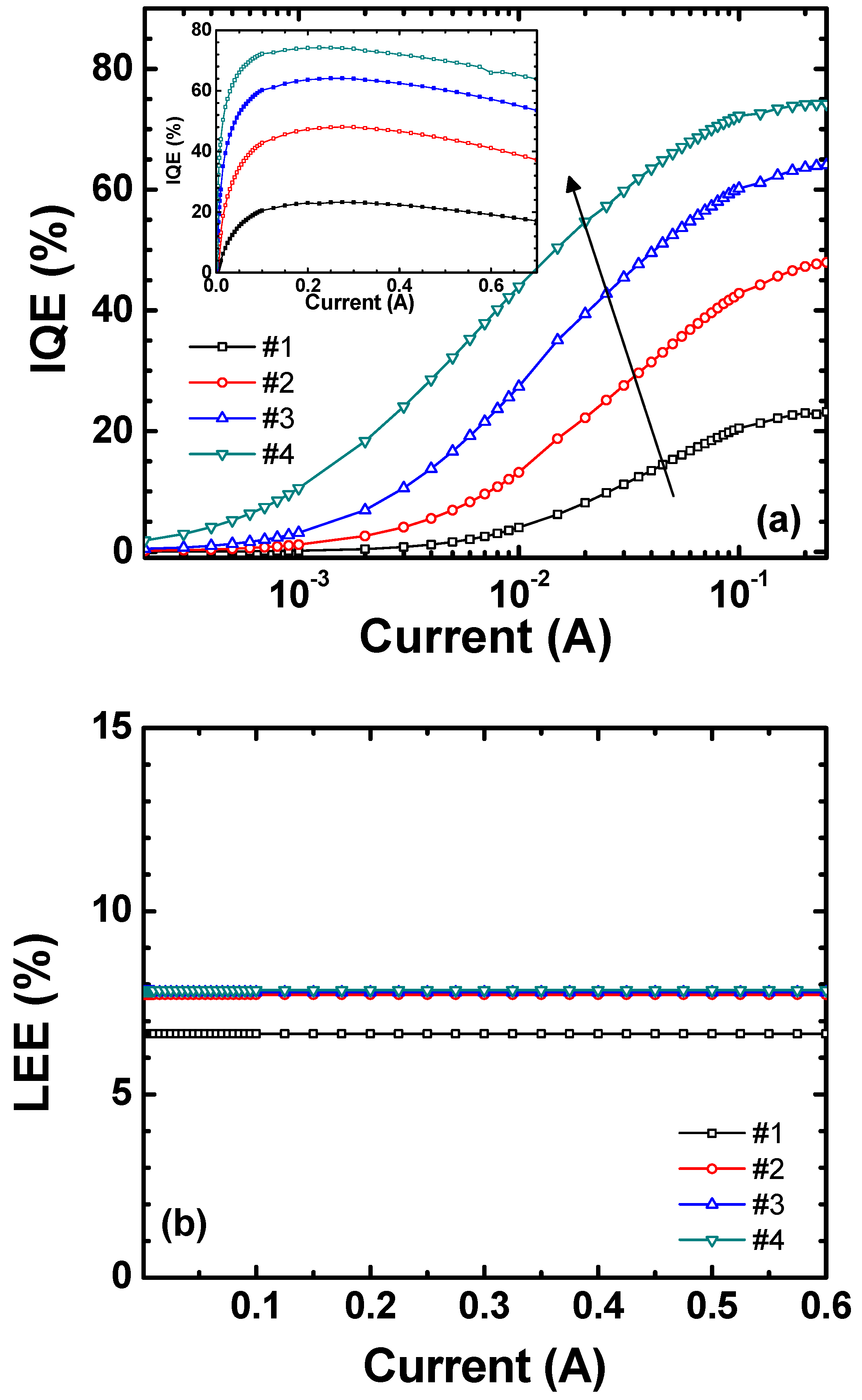
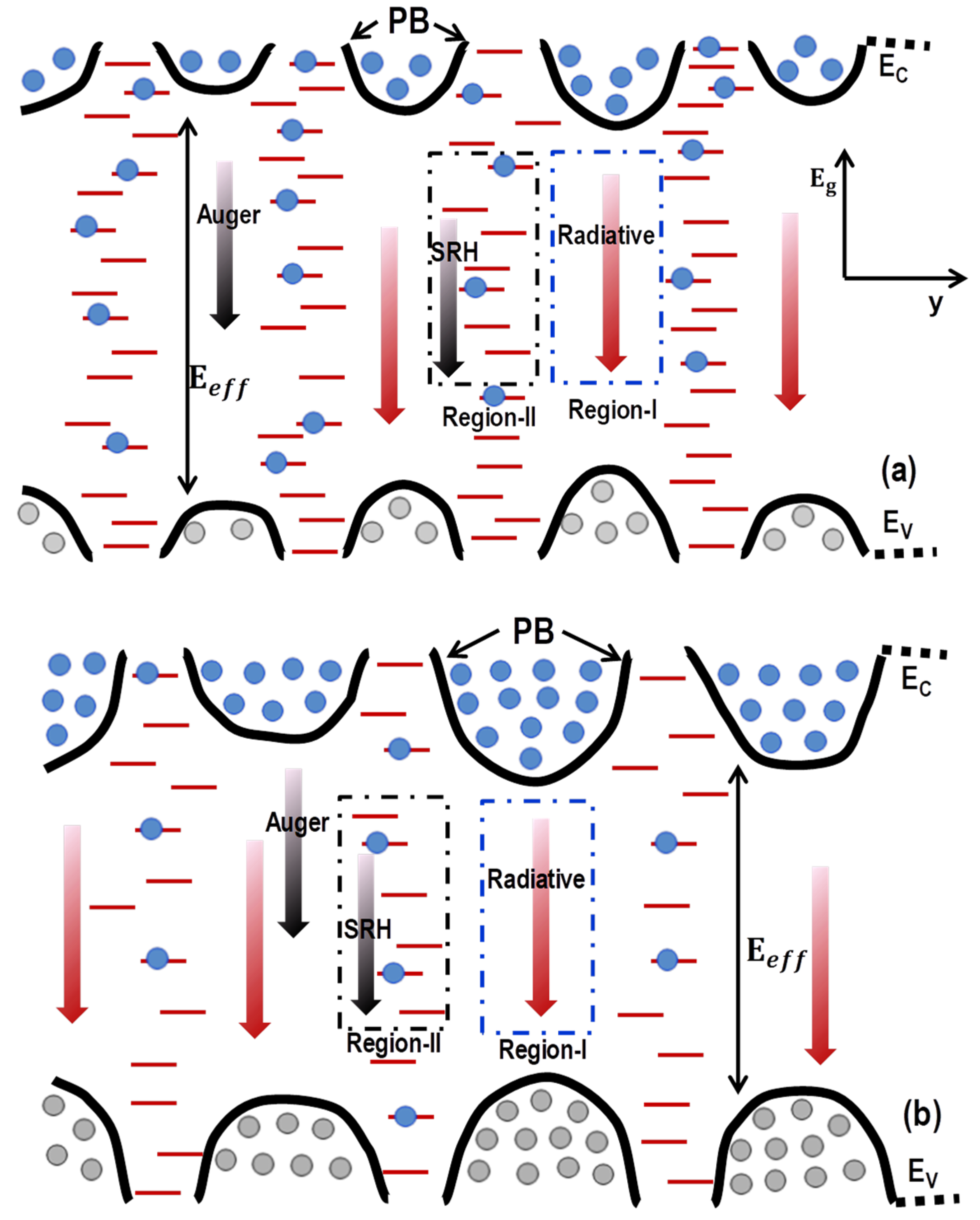
3. Results and Discussion

Figure 2 shows the I-V characteristics of the NUV LEDs measured by a Keithley semiconductor parameter analyzer, which was used to understand forward-bias voltage (VF), series resistance (RS) and forward leakages. As the sample’s In compositions increased, both VF and calculated RS [31] decreased as shown in Table 1. VF and RS decreased due to decreased bandgap energy and increased radiative recombination rates in the QWs [32]. The inset shows the ideality-factor characteristics calculated from the I-V data [33]. The values of the ideality factor, n, 1, 2, and >2 represent the carrier recombination mechanisms of band-to-band radiative recombination, SRH recombination through defects, and defect-assisted tunneling or surface recombination, respectively [33,34,35]. Both the tunneling and the SRH recombination via defects decreased from ~2.7 to 3.0 V for all samples except #1, which suffered from high defect-assisted tunneling under all applied biases. The minimum ideality factors (nmin), as shown in Table 1 indicate that the number of defects (especially point defects) in the QWs decreased with the sample’s In composition.
The carriers captured by the nonradiative recombination centers (NRCs) [25,34] caused by the point defects can also be reflected in the light-emission distribution shown in Figure 3, where the distributions were taken at a low current (1 µA), thus defects affecting emission properties. It was observed that the intensity in the EL distribution increased with the sample’s In composition. The increase in EL intensity or the radiative recombination rate with the sample number indicates that the number of point defects in the QWs decreased. Therefore, the decreased nmin, and the increased EL intensity reveal the improvement of crystal quality with the sample’s In composition.
The L-I characteristics of these NUV LEDs are shown in Figure 4a, where optical power was measured by a Si photodetector. These experiments were done in a pulse mode with 100 µm pulses and a 10% duty cycle to minimize the self-heating effect. Figure 4b shows the S characteristics of the samples, where the S values, obtained from the differential slope of log L vs. log I, indicate the dominant carrier-recombination mechanism at a given applied bias. The values of S > 2, 2, 1, and < 1 represent tunneling current, SRH recombination via defects, radiative recombination, and carrier leakage through overflow, respectively [36]. At a low current (10 mA), the sample’s S value decreased (see Table 1) due to the decrease in point defects, which is consistent with nmin and Figure 3. Thus, both the carrier tunneling from the QWs to the p-GaN layer and the SRH recombination through point defects decreased with the sample’s In composition. Furthermore, the overflow of electrons was suppressed at high currents due to the increase in conduction-band offset (ΔEC) with the sample’s In composition.
Figure 5a shows the normalized EL spectra and λp characteristics (inset) measured by the fiber-optic spectrometer (AvaSpec-2048). The sample’s λp increased owing to the decrease in bandgap energy. The decrease in defect density improved the radiative recombination rate that resulted in the sample’s EL intensity increase. As seen in the inset, all samples suffered from redshift due to bandgap narrowing (or shrinkage) caused by heat generation. The fact that the redshift decreased with the sample’s indium composition reflected the reduced heat produced by the carriers’ nonradiative recombination, namely SRH recombination [33,34] and tunneling from QWs [34,35] via point defects. No blueshift was observed at low currents. The blueshift was caused by the screening of FPZ (calculated through the ER spectroscopy seen in Table 1) due to localized carriers or band filling, both of which seem to be smaller than the redshift caused by heat generation.
The decrease in redshift at the current range from 1 to 350 mA was consistent with the fact that the number of point defects in QWs decreased with the sample’s In composition.
Figure 5b depicts the ER spectra at different biases for sample #1 used to find the flat-band voltage for calculating FPZ. The flat-band voltage was calculated by finding the phase inversion between the spectra as seen in Figure 5b [37]. The flat-band voltages thus obtained were 0.7, 0.5, 0.1 and −1.0 V for samples #1, #2, #3, and #4, respectively. The FPZ’s of these samples were calculated using the method described in Reference [38] with the device structure given above.
Differences in carrier recombination properties can be understood directly by analyzing IQE characteristics. The IQE is defined as the ratio of the number of photons emitted from the active region per second to the number of electrons injected into the active region per second. The IQEs of NUV LED samples have been calculated by using the fitting method of calculating IQE as described in Reference [39], which is shown in Figure 6a. The LEEs of these samples have also been calculated by using Reference [39]. Since LEE measures photon loss during propagation from the active region to free space [39], which is almost equal for all samples as seen in Figure 6b, the absorption of emitted photons by AlGaN barriers and GaN clad layers were similar for all samples [11]. For currents < 200 mA, the increase in IQE was caused by the increase in the radiative recombination rate, which is directly related to carrier localization and the effective radiative-recombination area in QWs. For the case of identical epitaxial structure, the increase in the radiative recombination rate at low currents before the IQE peak was due to the decrease in defects (especially the point defects in the active MQW region) since the defects act as NRCs for carriers, inducing SRH recombination [30] as reflected in the A coefficient. Again, the calculated A coefficient [39] decreased with the sample’s In composition (see Table 1), which is consistent with the PHEMOS patterns, nmin and S values at low currents. Thus, the effective radiative-recombination area increased with the reduction in point defects in QWs. Consequently, the SRH recombination and the tunneling from QWs through point defects decreased. As a result, IQE increased with the sample’s In composition. The increase in ΔEC reduced the carrier overflow from QWs, decreasing the sample’s IQE droop at high currents.
The analyses of I-V, nmin, the PHEMOS pattern, the S value, the EL spectrum, λp, the ER, and the IQE indicated that as the sample’s In composition, number of point defects, SRH recombination rate, carrier tunneling and overflow, and redshift all decreased; ΔEC, crystal quality, and FPZ all increased (as listed in Table 1). The improvement of the optoelectronic performances mentioned above increased the sample’s radiative recombination rate. However, it needs to be clarified which factor dominantly increased the radiative recombination rate at low currents. In this work, we propose that the dominant factor was spatially localized carriers caused by in-plane potential-energy fluctuation in QWs [18,19,20,21,22,23,24,25,26,27,28,29,30].
The possible reason for the potential-energy fluctuation could be the combined effects of inhomogeneous distribution of point defects, which was strongly affected by FPZ, and In composition: Schematic diagrams depicted in Figure 7 systematically and interactively describe the situation. There were inhomogeneously distributed point defects [40] caused by Ga/N vacancies [14,41] in QWs, which were not filled up by neighboring atoms with strong bonds between other atoms. This effect relaxed the neighboring atoms by increasing the lattice constant, which led to the bandgap energy near the point defect increasing [30,33]. Thus, in a site with accumulated defects, the crystal relaxation occurs and the bandgap energy near this site increased like a potential barrier (PB). Thus, a relatively defect-free potential “valley” was created between the accumulated defective sites. In these potential valleys, carriers were localized as depicted in Figure 7 [30]. Note that the number of defects were much smaller in the potential valley, with better crystal quality that yielded higher strain [30]. Thus, FPZ increases around the potential valley that seems to cause the PB height surrounding the defects to increase.
On the other hand, the strain near the defects was relaxed owing to the missing atoms. Hence, FPZ would be smaller at the defective region. The point defects always changed the uniform distribution of In atoms over the QWs. Therefore, the In composition in the potential valley would be higher than in the defect sites. Since the effective bandgap energy decreased with In composition [27,33] and FPZ, in the potential-valley area, the depth and PB height increased with the sample’s In composition.
The distribution of potential valleys broke the uniform potential and resulted in the phenomenon of potential-energy fluctuation in QWs. This potential-energy fluctuation in QWs increased with In composition, which led to increased carrier localization states in the QWs. Moreover, PB prevented carriers from diffusing into defects due to higher potential at the edge of the defects [13,16,25,26,30]. Consequently, carrier localization increased the local carrier density in the QWs [13]. Recent studies showed that the hole wavefunction is more localized compared to the electron wavefunction for the potential-energy fluctuation [20,21]. These localized carriers increased the QW occupancy factor. As a result, these carriers radiatively recombined in Region I due to the decrease in the SRH process via point defects, which explains the improved radiative recombination (or the IQE) in these LEDs.
The differences in macroscopic optoelectronic characteristics of NUV LED samples with identical epitaxial layers except for In composition, as summarized in Table 1, can be consistently understood by using the proposed model of local in-plane potential fluctuation in the QWs as depicted in Figure 7. At low currents, the injected carriers in the active region always have three different kinds of processes. The first process is localization of carriers at the valleys that mostly cause radiative recombination; the second process is the capture of carriers by point defects (i.e., NRCs) that cause SRH nonradiative recombination, and the last process is the tunneling of carriers from QWs through the point defects to the p-GaN layer that yields additional nonradiative recombination. At low currents, such as 0.5 mA, the radiative recombination rate increased with the sample’s In composition due to the influence of local in-plane potential fluctuation (deeper valleys and, thus, higher carrier density) since more electron-hole pairs were available for radiative recombination. As the current increased to ~150 mA, the IQEs of all samples increased due to the increment of the radiative recombination rate over the nonradiative recombination rate (caused by the SRH and tunneling processes). This observation is consistent with S values decreasing with reduced point defects owing to the increased In composition. In this current region, the overall IQE increased with the sample’s In composition, caused by the decreasing point defects (which was also consistent with the calculated A coefficients, S values, and the PHEMOS patterns). The maximum IQE increased with the sample’s In composition, which was due to reduced NRCs in potential valleys and the increased area of potential valleys in QWs.

4. Conclusions

In summary, it has been investigated that the increased radiative recombination rate in the InGaN-based NUV LEDs was caused by the localized states owing to the potential-energy fluctuation in the QWs. The decrease in point defects in the QWs was consistently confirmed through the analyses of nmin, the SRH coefficient, the PHEMOS distribution, and the S value. At low currents, the decrease in the sample’s redshift was attributed to the decreased SRH recombination and carrier tunneling. A consistent relationship between the S value and the IQE was also found via the decrease in SRH recombination and the carrier tunneling at low current and carrier overflow at high currents. At low currents, the increased radiative recombination rate was caused especially by the carrier localization via potential-energy fluctuation in the QWs that reduced SRH recombination and carrier tunneling from the QWs to the p-GaN clad layer through point defects. The origin of the potential-energy fluctuation was considered to be from the combined effects of the inhomogeneous distribution of point defects, FPZ, and the In composition, which has been consistently comprehended by using macroscopic characterizations. This work emphasizes that the potential-energy fluctuation in QWs plays a very important role in the performance of LEDs, especially NUV LEDs.

Author Contributions

A.B.M.H.I. conducted the experiments and data analysis under guidance of J.-I.S. and D.-S.S.; A.B.M.H.I. wrote the manuscript and J.-I.S. and D.-S.S. read, edited, and commented on the manuscript.

Funding

This work was supported by the Technology Innovation Program (Grant 10065712) funded by the Ministry of Trade, Industry and Energy, Republic of Korea.

Acknowledgments

The authors are grateful to Joosun Yun for the help in the analyses of the IQE curves.

Conflicts of Interest

The authors declare no conflicts of interest.

References

  1. Sandhu, A. The future of ultraviolet LEDs. Nat. Photonics 2007, 1, 38. [Google Scholar] [CrossRef]
  2. Kuo, Y.-K.; Shih, Y.-H.; Tsai, M.-C.; Chang, J.-Y. Improvement in Electron Overflow of Near-Ultraviolet InGaN LEDs by Specific Design on Last Barrier. IEEE Photonics Technol. Lett. 2011, 23, 1630–1632. [Google Scholar] [CrossRef]
  3. Li, P.; Li, H.; Wang, L.; Yi, X.; Wang, G. High Quantum Efficiency and Low Drop of 400-nm InGaN Near-Ultraviolet Light-Emitting Diodes through Suppressed Leakage Current. IEEE J. Quantum Electron. 2015, 51, 3300605. [Google Scholar] [CrossRef]
  4. Muramoto, Y.; Kimura, M.; Nouda, S. Development and future of ultraviolet light-emitting diodes: UV-LED will replace the UV lamp. Semicond. Sci. Technol. 2014, 29, 084004. [Google Scholar] [CrossRef]
  5. Kipshidze, G.; Kuryatkov, V.; Borisov, B.; Holtz, M.; Nikishin, S.; Temkin, H. AlGaInN-based ultraviolet light-emitting diodes grown on Si (111). Appl. Phys. Lett. 2002, 80, 3682–3684. [Google Scholar] [CrossRef]
  6. Khan, A.; Balakrishnan, K.; Katona, T. Ultraviolet light-emitting diodes based on group three nitrides. Nat. Photonics 2008, 2, 77–84. [Google Scholar] [CrossRef]
  7. Kneissl, M.; Kolbe, T.; Chua, C.; Kueller, V.; Lobo, N.; Stellmach, J.; Knauer, A.; Rodriguez, H.; Einfeldt, S.; Yang, Z.; et al. Advances in group III-nitride-based deep UV light-emitting diode technology. Semicond. Sci. Technol. 2011, 26, 014036. [Google Scholar] [CrossRef]
  8. Sintov, Y.; Malka, D.; Zalevsky, Z. Prospects for diode pumped alkali atom based hollow core photonic crystal fiber lasers. Opt. Lett. 2014, 39, 4655–4658. [Google Scholar] [CrossRef] [PubMed]
  9. Malka, D.; Cohen, E.; Zalevsky, Z. Design of 4 × 1 power beam combined based on multicore photonic crystal fiber. Appl. Sci. 2017, 7, 695. [Google Scholar] [CrossRef]
  10. Meneghini, M.; Pavesi, M.; Trivellin, N.; Gaska, R.; Zanoni, E.; Meneghesso, G. Reliability of deep-UV light-emitting diodes. IEEE Trans. Device Mater. Reliab. 2008, 8, 248–254. [Google Scholar] [CrossRef]
  11. Maeda, N.; Hirayama, H. Realization of high-efficiency deep-UV LEDs using transparent p-AlGaN contact layer. Phys. Status Solidi C 2013, 10, 1521–1524. [Google Scholar] [CrossRef]
  12. Fu, Y.-K.; Jiang, R.-H.; Lu, Y.-H.; Chen, B.-C.; Xuan, R.; Fang, Y.-H.; Lin, C.-F.; Su, Y.-K.; Chen, J.-F. The effect of trimethylgallium flows in the AlInGaN barrier on optoelectronic characteristics of near ultraviolet light-emitting diodes grown by atmospheric pressure metalorganic vapor phase epitaxy. Appl. Phys. Lett. 2011, 98, 121115. [Google Scholar] [CrossRef]
  13. Nakamura, S. The Roles of Structural Imperfections in InGaN-Based Blue Light-Emitting Diodes and Laser Diodes. Science 1998, 281, 956–961. [Google Scholar] [CrossRef] [Green Version]
  14. Reshchikov, M.A.; Morkoc, H. Luminescence properties of defects in GaN. J. Appl. Phys. 2005, 97, 061301. [Google Scholar] [CrossRef]
  15. Hirsch, L.; Barriere, A.S. Electrical characterization of InGaN/GaN light emitting diodes grown by molecular beam epitaxy. J. Appl. Phys. 2003, 94, 5014–5520. [Google Scholar] [CrossRef]
  16. Chichibu, S.F.; Uedono, A.; Onuma, T.; Haskell, B.A.; Chakraborty, A.; Koyama, T.; Fini, P.T.; Keller, S.; Denbaars, S.P.; Speck, J.S.; et al. Origin of defect-insensitive emission probability in In-containing (Al,In,Ga)N alloy semiconductors. Nat. Mater. 2006, 5, 810–816. [Google Scholar] [CrossRef] [PubMed]
  17. Davidson, J.; Dawson, P.; Wang, T.; Sugahara, T.; Orton, J.; Sakai, S. Photoluminescence studies of InGaN/GaN multi-quantum wells. Semicond. Sci. Technol. 2000, 15, 497–505. [Google Scholar] [CrossRef]
  18. Wu, Y.-R.; Shivaraman, R.; Wang, K.-C.; Speck, J.S. Analyzing the physical properties of InGaN multiple quantum well light emitting diodes from nano scale structure. Appl. Phys. Lett. 2012, 101, 083505. [Google Scholar] [CrossRef]
  19. Yang, T.-J.; Shivaraman, R.; Speck, J.S.; Wu, Y.-R. The influence of random indium alloy fluctuations in indium gallium nitride quantum wells on the device behavior. J. Appl. Phys. 2014, 116, 113104. [Google Scholar] [CrossRef]
  20. Watson-Parris, D.; Godfrey, M.J.; Dawson, P.; Oliver, R.A.; Galtrey, M.J.; Kappers, M.J.; Humphreys, C.J. Carrier localization mechanisms in InxGa1−xN/GaN quantum wells. Phys. Rev. B 2011, 83, 115321. [Google Scholar] [CrossRef]
  21. Schulz, S.; Caro, M.A.; Coughlan, C.; O’Reilly, E.P. Atomistic analysis of the impact of alloy and well-width fluctuations on the electronic and optical properties of InGaN/GaN quantum wells. Phys. Rev. B 2015, 91, 035439. [Google Scholar] [CrossRef] [Green Version]
  22. Bellaiche, L.; Mattila, T.; Wang, L.-W.; Wei, S.-H.; Zunger, A. Resonant hole localization and anomalous optical bowing in InGaN alloys. Appl. Phys. Lett. 1999, 74, 1842–1844. [Google Scholar] [CrossRef]
  23. Cheng, Y.-C.; Lin, E.-C.; Wu, C.-M.; Yang, C.C.; Yang, J.-R.; Rosenauer, A.; Ma, K.-J.; Shi, S.-C.; Chen, L.C.; Pan, C.-C.; et al. Nanostructures and carrier localization behaviors of green-luminescence InGaN/GaN quantum-well structures of various silicon-doping conditions. Appl. Phys. Lett. 2004, 84, 2506–2508. [Google Scholar] [CrossRef]
  24. Jeong, H.; Jeong, H.J.; Oh, H.M.; Hong, C.-H.; Suh, E.K.; Lerondel, G.; Jeong, M.S. Carrier localization in In-rich InGaN/GaN multiple quantum wells for green light-emitting diodes. Sci. Rep. 2015, 5, 9373. [Google Scholar] [CrossRef] [PubMed]
  25. Hader, J.; Moloney, J.V.; Koch, S.W. Density-activated defect recombination as a possible explanation for the efficiency droop in GaN-based diodes. Appl. Phys. Lett. 2010, 96, 221106. [Google Scholar] [CrossRef]
  26. Hangleiter, A.; Hitzel, F.; Netzel, C.; Fuhrmann, D.; Rossow, U.; Ade, G.; Hinze, P. Suppression of nonradiative recombination by V-shaped pits in GaInN/GaN quantum wells produces a large inncrease in the light emission efficiency. Phys. Rev. Lett. 2005, 95, 1274702. [Google Scholar] [CrossRef] [PubMed]
  27. Kudrawiec, R.; Siekacz, M.; Krysko, M.; Cywinski, G.; Misiewicz, J.; Skierbiszewski, C. Contactless electroreflectance of InGaN layers with indium content ≤36%: The surface band bending, band gap bowing, and Stokes shift issues. J. Appl. Phys. 2009, 106, 113517. [Google Scholar] [CrossRef]
  28. Ponce, F.A.; Srinivasan, S.; Bell, A.; Geng, L.; Liu, R.; Stevens, M.; Cai, J.; Omiya, H.; Marui, H.; Tanaka, S. Microstructure and electronic properties of InGaN alloys. Phys. Status Solidi B 2003, 240, 273–284. [Google Scholar] [CrossRef]
  29. Pereira, S.; Correia, M.R.; Perira, E.; Trager-Cowan, C.; Sweeney, F.; O’Donnell, K.P.; Alves, E.; Franco, N. Sequeira Structural and optical properties of InGaN/GaN layers close to the critical layer thickness. Appl. Phys. Lett. 2002, 81, 1207. [Google Scholar] [CrossRef]
  30. Islam, A.B.M.H.; Shim, J.-I.; Shin, D.-S. Optoelectronic performance variations in InGaN/GaN multiple-quantum-well light-emitting diodes: Effects of potential fluctuation. Materials 2018, 11, 743. [Google Scholar] [CrossRef] [PubMed]
  31. Tu, P.-M.; Chang, C.-Y.; Huang, S.-C.; Chiu, C.-H.; Chang, J.-R.; Chang, W.-T.; Wuu, D.-S.; Zan, H.-W.; Lin, C.-C.; Kuo, H.-C.; et al. Investigation of efficiency droop for InGaN-based UV light-emitting diodes with InAlGaN barrier. Appl. Phys. Lett. 2011, 98, 211107. [Google Scholar] [CrossRef]
  32. Lee, G.W.; Shim, J.-I.; Shin, D.-S. On the ideality factor of the radiative recombination current in semiconductor light-emitting diodes. Appl. Phys. Lett. 2016, 109, 031104. [Google Scholar] [CrossRef]
  33. Schubert, E.F. Light-Emitting Diodes; Cambridge University Press: Cambridge, UK, 2006; Chapter 4. [Google Scholar]
  34. Seong, T.-Y.; Han, J.; Amano, H.; Morkoc, H. III-Nitride Based Light Emitting Diodes and Applications; Springer: Heidelberg, Germany, 2013; p. 153. [Google Scholar]
  35. Bochkareva, N.I.; Voronenkov, V.V.; Gorbunov, R.I.; Zubrilov, A.S.; Lelikov, Y.S.; Latyshev, P.E.; Rebane, Y.T.; Tsyuk, A.I.; Shreter, Y.G. Defect-related tunneling mechanism of efficiency droop in III-nitride light-emitting diodes. Appl. Phys. Lett. 2010, 96, 133502. [Google Scholar] [CrossRef]
  36. Han, D.-H.; Oh, C.-H.; Zheng, D.-G.; Kim, H.; Shim, J.-I.; Kim, K.-S.; Shin, D.-S. Analysis of nonradiative recombination mechanisms and their impacts on the device performance of InGaN/GaN light-emitting diodes. Jpn. J. Appl. Phys. 2015, 54, 02BA01. [Google Scholar] [CrossRef]
  37. Islam, A.B.M.H.; Shim, J.-I.; Shin, D.-S. Interactive study of electroreflectance and photocurrent spectra in InGaN/GaN-based blue LEDs. IEEE J. Quantum Electron. 2017, 53, 3300206. [Google Scholar] [CrossRef]
  38. Park, S.-I.; Lee, J.-I.; Jang, D.-H.; Kim, H.-S.; Shin, D.-S.; Ryu, H.-Y.; Shim, J.-I. Measurement of internal electric field in GaN-based light-emitting diodes. IEEE J. Quantum Electron. 2012, 48, 500–506. [Google Scholar] [CrossRef]
  39. Yun, J.; Shim, J.-I.; Hirayama, H. Analysis of efficiency droop in 280-nm AlGaN multiple-quantum-well light-emitting diodes based on carrier rate equation. Appl. Phys. Express 2015, 8, 022104. [Google Scholar] [CrossRef]
  40. Reshchikov, M.A.; Yi, G.-C.; Wessels, B.W. Behavior of 2.8- and 3.2-eV photoluminescence bands in Mg-doped GaN at different temperatures and excitation densities. Phys. Rev. B 1999, 59, 13176–13183. [Google Scholar] [CrossRef]
  41. Van de Walle, C.G.; Neugebauer, J. First-principles calculations for defects and impurities: Applications to III-nitrides. J. Appl. Phys. 2004, 95, 3851–3879. [Google Scholar] [CrossRef]
Figure 1. Schematic structure of the light-emitting diode (LED) samples under study.
Applsci 09 00871 g001
Figure 2. Current-voltage (I-V) characteristics of the LED samples. The inset shows the calculated ideality factor (n) characteristics.
Applsci 09 00871 g002
Figure 3. Light-emission patterns of NUV LEDs at 1 µA (~2.4 V) measured by a Hamamatsu PHEMOS-1000 system.
Applsci 09 00871 g003
Figure 4. (a) Light power vs. current (L-I) characteristics and (b) S values calculated from the measured L-I characteristics for all samples, where #1 suffers from severe overflow of electrons owing to the low band offset.
Applsci 09 00871 g004
Figure 5. (a) Normalized electroluminescence (EL) spectra at 350 mA and room temperature, where all the samples’ peak intensities are normalized with respect to that of #4. The inset shows the peak wavelength characteristics. (b) Electroreflectance (ER) spectra at different biases for sample #1.
Applsci 09 00871 g005
Figure 6. (a) The IQE characteristics on a semi-log scale from 200 µA to 250 mA. The inset shows the IQE characteristics from 200 µA to 700 mA on a linear scale. (b) The calculated LEE efficiencies.
Applsci 09 00871 g006
Figure 7. Schematic illustration of the proposed local in-plane fluctuation of potential energy in the quantum wells (QWs) for (a) #1 and (b) #4, where PB represents the potential barrier. Regions I and II represent the radiative recombination and the SRH process or carrier tunneling via point defects, respectively.
Applsci 09 00871 g007
Table 1. Device characteristics of the near-ultraviolet (NUV) LED samples under study. VF: Forward-bias voltage at 220 mA (20 A/cm2); RS: Series resistance; nmin: Minimum ideality factor; A: The Shockley–Read–-Hall (SRH) recombination coefficient; Eg: Bandgap energy calculated from Vegard’s Law, where the bandgap energies of GaN, InN, AlN, and bowing parameters of InGaN and AlGaN are 3.44, 0.72, 6.28, 1.3, and 0.8 eV, respectively; ΔEC: Conduction-band offset; FPZ: Piezoelectric field; λ350: Peak wavelength at 350 mA; λ1: Peak wavelength at 1 mA; S10: S value at 10 mA; S450: S value at 450 mA, which represents carrier overflow; LEE: Relative light extraction efficiency; IQEmax: Maximum internal quantum efficiency (IQE).
-#1#2#3#4
In composition (%)4.55.56.57.5
VF (V)3.683.533.513.47
RS (Ω)2.01.91.81.7
nmin2.71.91.81.6
A (×107 s−1)3.241.721.000.62
Eg (eV)~3.26~3.22~3.18~3.15
ΔEC (eV)~0.50~0.54~0.58~0.62
Fpz (MV/cm)−0.8−0.9−1.0−1.1
λ350 (nm)379.0386.6392.9397.2
λ1 (nm)374.6382.8389.8395.0
Redshift (nm)4.43.83.12.2
S10 (a.u.)2.11.71.51.3
S450 (a.u.)0.680.760.840.86
LEE (%)6.657.717.787.84
IQEmax (%)23.248.064.174.2

