Article

Improving the Lot Fabrication Stability and Performance of Silica Optical Films during PECVD

1
State Key Laboratory of High Performance Complex Manufacturing, College of Mechanical and Electrical Engineering, Central South University, Changsha, Hunan 410083, China
2
Hunan Institute of Technology, Hengyang 421002, China
3
Hunan New Fiber Optical Electronics Co., Ltd., Baojing, Hunan 416500, China
*
Authors to whom correspondence should be addressed.
Appl. Sci. 2019, 9(4), 785; https://doi.org/10.3390/app9040785
Submission received: 19 December 2018 / Revised: 18 February 2019 / Accepted: 19 February 2019 / Published: 22 February 2019
(This article belongs to the Special Issue Photonic Integrated Circuits for Optical Communications)

Abstract

:
Silica optical film specifications are determined by their processing capability and their fabrication stability. Here, a statistical process control (SPC) approach usually used in planar lightwave circuits (PLC) is adopted to analyze the stability of the silica optical film fabrication process. Apart from the raw materials, certain key external factors have to be taken into consideration during the PLC process, such as temperature, relative humidity, process variation and machine aging. The fabrication process can be adjusted according to SPC-based results in real-time, so as to produce high quality silica optical film. By using this method, it is possible to assess the effectiveness of older production lines and extend their production capacity at minimal cost.

1. Introduction

Following recent developments in planar lightwave circuits (PLC), silica optical waveguides have come to play an important role in optical fiber communications and optical fiber sensor systems. They offer a number of notable advantages, including low propagation loss, low fiber-to-chip loss, an adjustable refractive index, good integration capability and high mechanical stability [1,2,3]. There are various silica optical waveguide devices, including 1 × N (N = 2, 4, 8, 16, 32, 64… …) power splitters, arrayed waveguide gratings (AWG), variable optical attenuators (VOA), ring resonators and star couplers, all of which have been successfully fabricated using PLCs [4,5]. A silica optical waveguide consists of a core layer, an upper cladding layer and a lower cladding layer. The core layer has a high refractive index (RI), whilst the cladding layers have a lower RI. Their low propagation loss is a particularly important property of silica optical waveguides. Typically, this is lower than 0.1 dB/cm. Similarly, they have a low fiber-to-chip coupling loss of less than 0.1 dB/point and a low RI contrast (Δ = 0.25–1.5%) [6,7,8]. Usually, silica optical waveguides are fabricated using Si or a fused silica substrate. The fabrication process includes the lower cladding layer deposition, the core layer deposition, a masking deposition, photolithography, the core etching and the upper layer deposition. Silica optical films can be used for the core layer, lower cladding layer and upper cladding layer [7,8]. By adding materials such as germanium (GeO2-SiO2), phosphorous (P2O5-SiO2), nitrogen (SiON-SiO2) and boron (B2O3-SiO2), or a combination of these materials, silica optical films can be used to precisely adjust the RI. Their thickness and residual stress can be controlled during the processing phase. They can be fabricated by means of thermal oxidation and chemical vapor deposition (CVD). The latter can include atmospheric pressure CVD (APCVD), low pressure CVD (LPCVD), plasma enhanced CVD (PECVD) and electron cyclotron resonance CVD (ECRCVD), or a combination of these methods [9,10,11,12]. Flame hydrolysis deposition (FHD) and a sol gel method can also be used [12,13]. Out of all of these methods, PECVD offers particular advantages. This is because of its ability to control the RI, thickness, residual stress and surface roughness [14,15]. A lot of research has been devoted to studying the relationship between various process parameters (Radio frequency power, gas flow, chamber temperature, chamber pressure, etc.) and the quality of the film (RI, film thickness, etc.) [14,15]. However, very few papers have examined the relationship and process stability between them in lot fabricating.
In this paper, we focus on lot fabrication stability using PECVD for GeO2-SiO2-based silica optical films in relation to certain key parameters, such as the RI and film thickness. This can be used to determine how well the fabrication process will cope with the required tolerances, for the selection or modification of the fabrication process during optical waveguide design, for the specification of the processing requirements for PECVD machines and, above all, to reduce variability in the fabrication process.

2. Lot Fabrication

A 6 μM ± 0.4 μM thick GeO2-SiO2 optical film was deposited on 23 lots (with 15 pieces per lot) of 6″ fused quartz wafers, 1 mm thick and 1.4574 at 632.8 nm. The RI contrast between the core layer and the cladding layer was 0.36% (Δ = 0.36% ± 0.05%). The GeO2-SiO2 optical film was produced by means of SiH4/GeH4/N2O high density plasma chemistry in an AMAT CENTRUA 5200 PECVD machine, where the plasma was generated at 13.56 MHz. The plasma parameters were fixed as follows: An RF (Radio frequency) power of 350 W; a processing pressure of 2.7 Torr; an electrode and wafer gap of 450 mils (11430 μM); a wafer temperature of 350 °C; and a chamber wall temperature of 60 °C. The other processing parameters were as follows: A SiH4 flow of 40 sccm; a GeH4 (combined with 95% H2) flow of 72 sccm; and a N2O flow of 2500 sccm. The deposition time was set to 1090 s. Each wafer was complete after the PECVD deposition. The deposition chamber was cleaned by running 20 cycles of a standard plasma cleaning process with the gas CF4. After the PECVD deposition process, the wafers were annealed at 1100 °C for 2 h.
One lot of the fused quartz wafers was subjected to deposition each day for 23 days, so that we ended up with a total of 345 wafers. The GeO2-SiO2 optical film’s RI was measured using a prism coupling instrument and its thickness was measured using a film thickness gauge. The measurement error was approximately ±0.0001 for the RI and ±0.1% for the thickness. For each wafer, five positions (T for top, C for center, B for bottom, R for right and L for left) were measured on the wafer and the RI and thickness values were analyzed. RI-T, RI-C, RI-B, RI-R and RI-L refer to the RI of the top, center, bottom, right and left points on each wafer, respectively. THK-T, THK-C, THK-B, THK-R and THK-L refer to the thickness of the layer at the top, center, bottom, right and left points on each wafer, respectively.

3. Results and Discussion

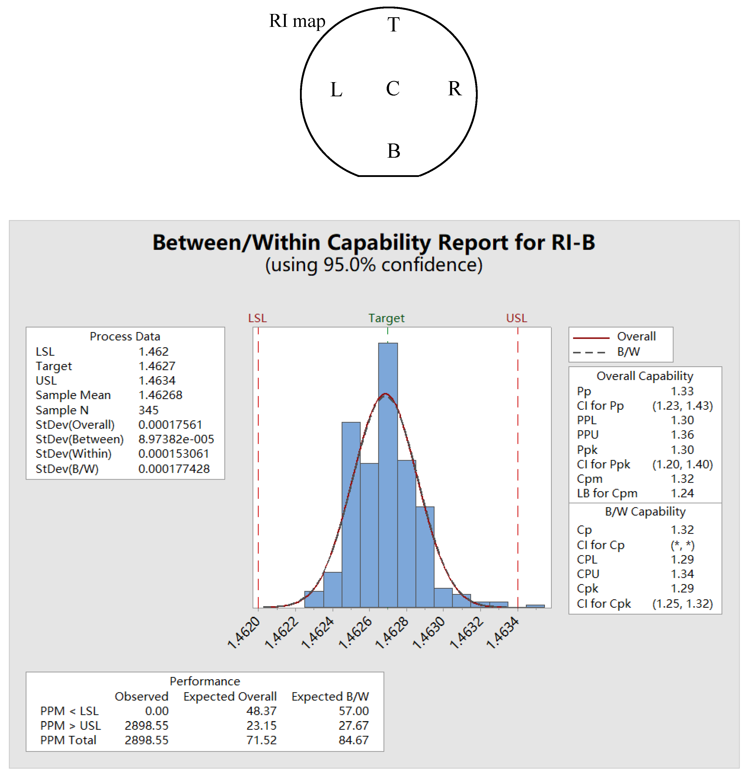
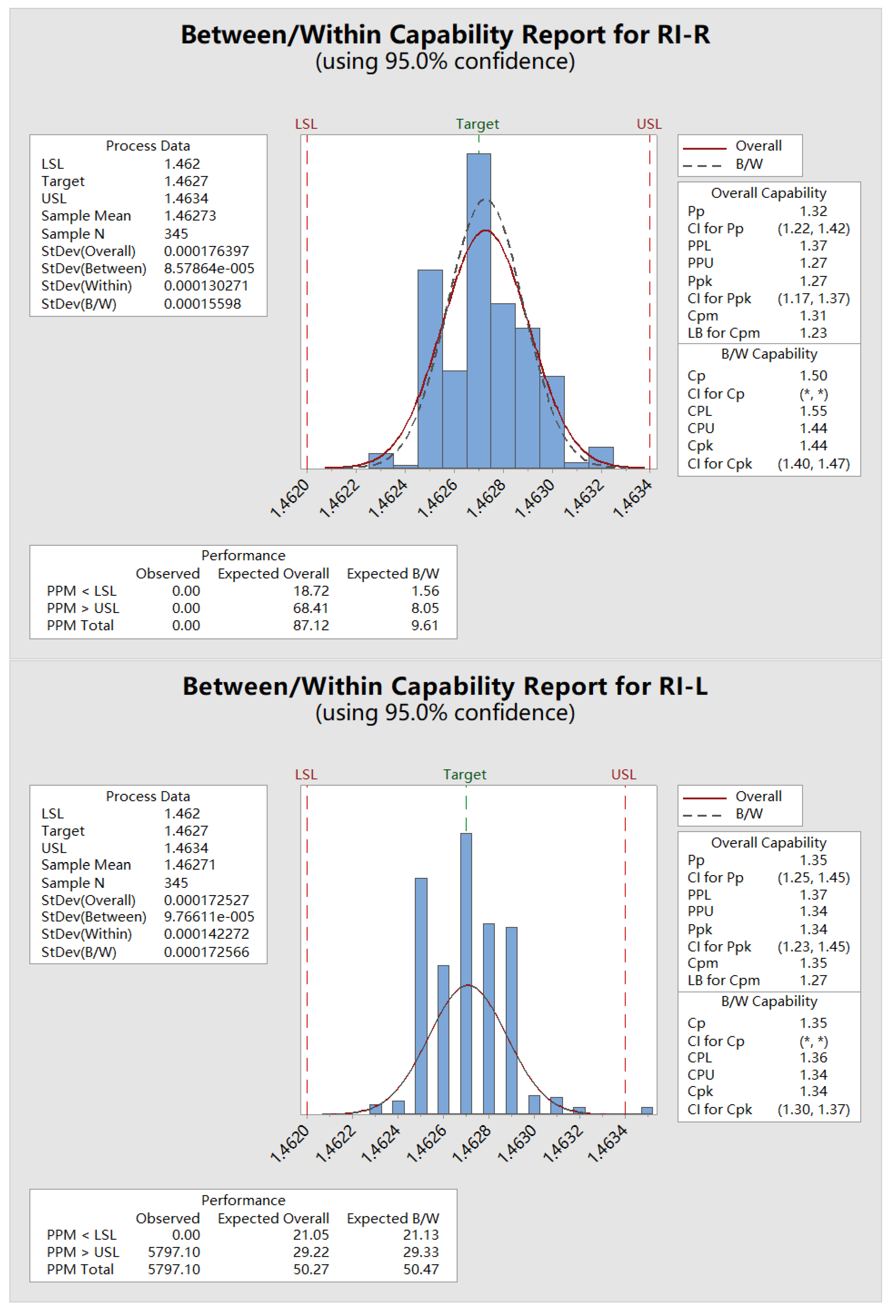
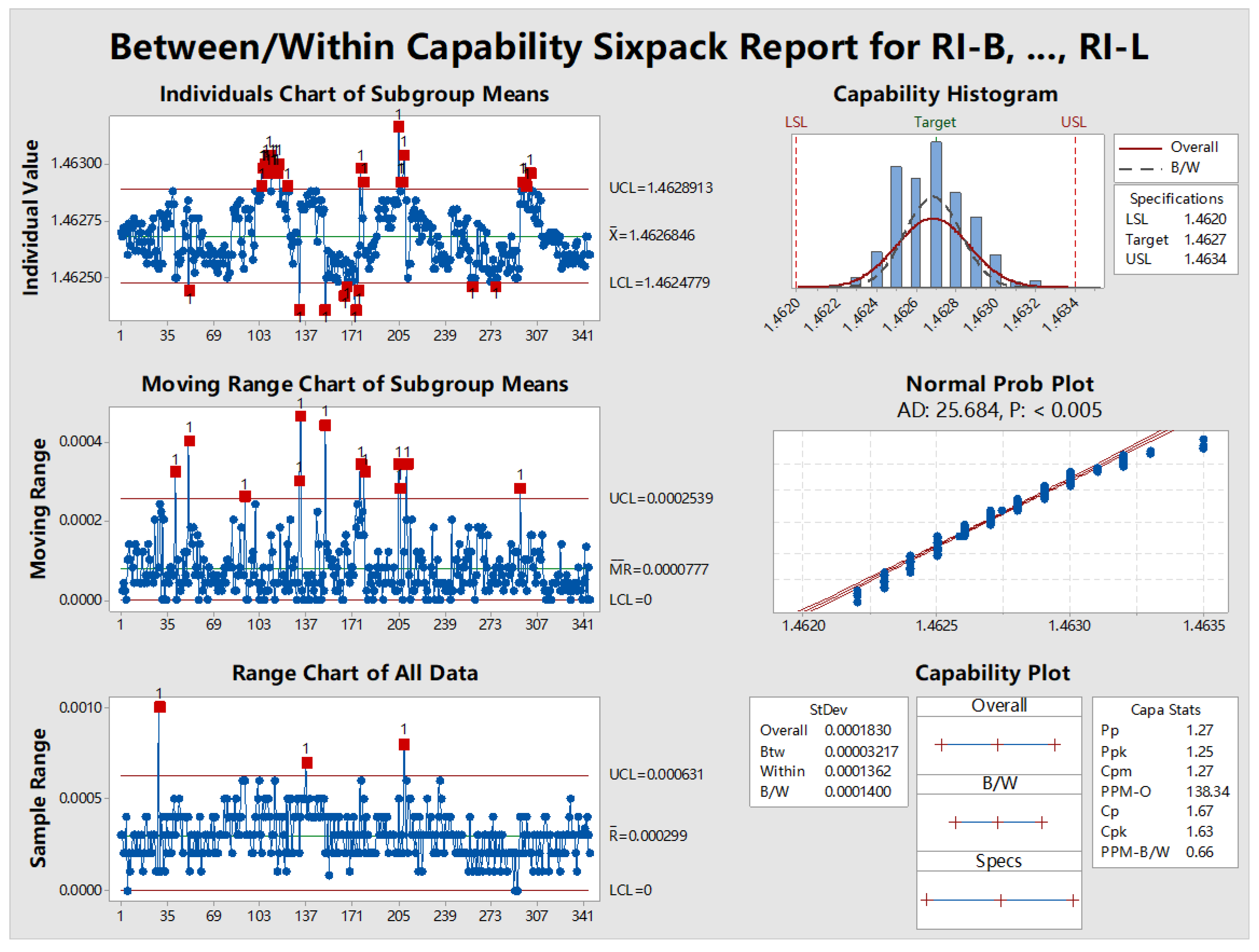
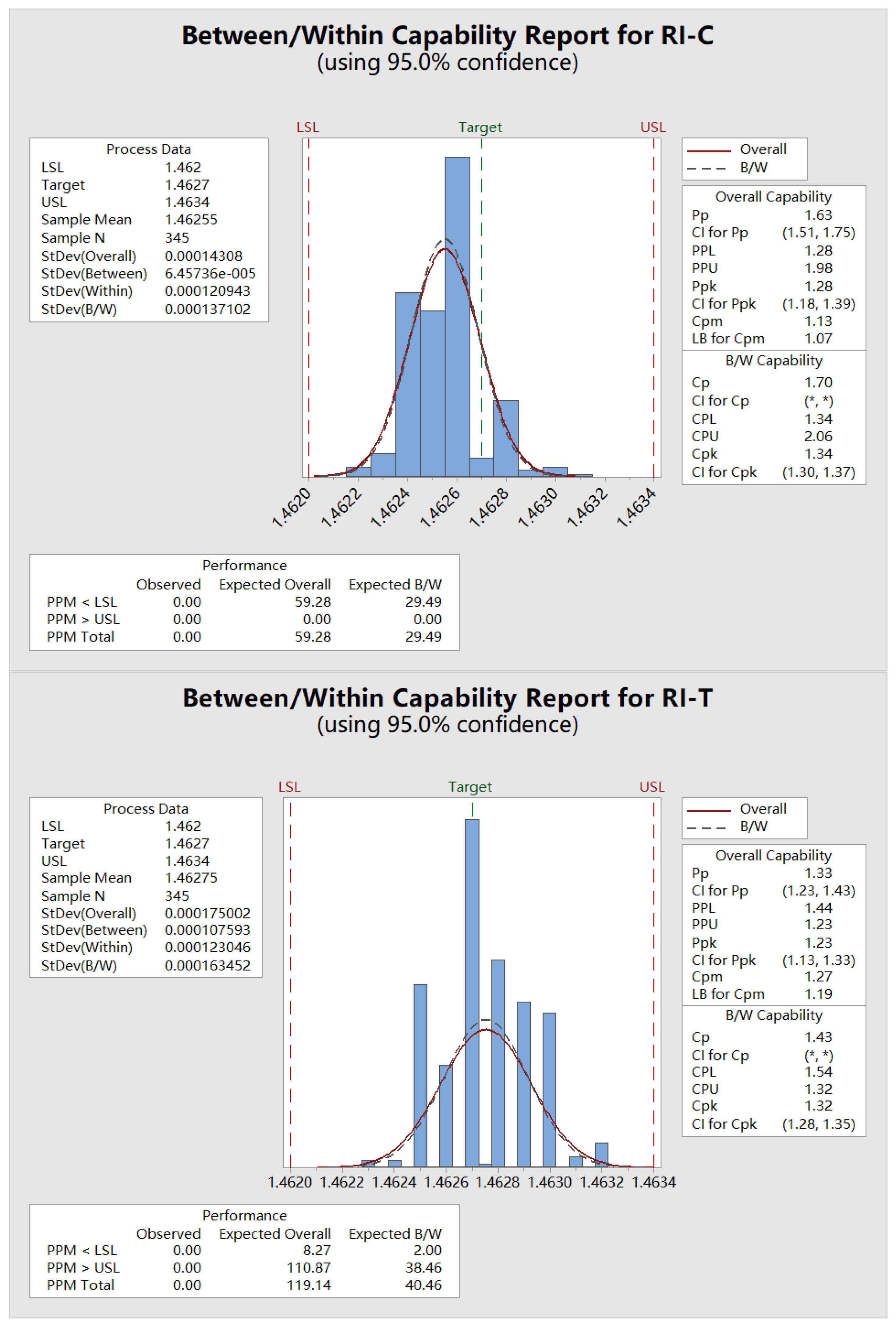
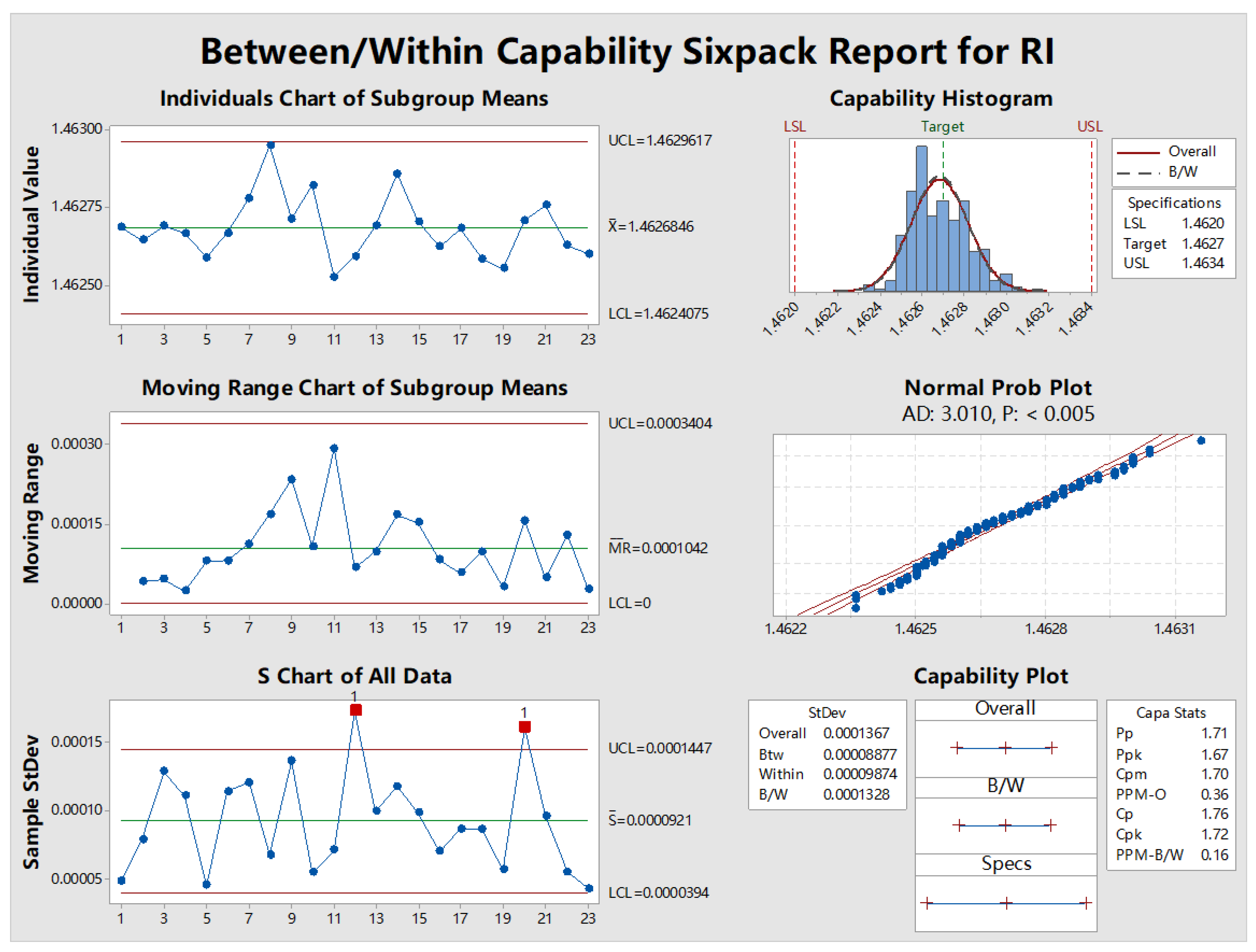
3.1. RI of the GeO2-SiO2 Optical Film

Figure 1 shows the RI maps and histograms for the 345 wafers with their specification limits and targets for RI-B, RI-C, RI-T, RI-R and RI-L. According to the requirements for silica optical waveguides, the lowest specification limit for the RI was set at 1.4620, the highest specification limit was set to 1.4634 and the RI target was set to 1.4627. The data presented in Figure 1 suggests the wafers were very close to having a normal distribution. The RI for RI-B, RI-R and RI-L were closest to the RI target. The RI for RI-C was lower than the RI target and the RI for RI-T was higher than the RI target. Cp is a measure of the potential capability of the process. Cp = (USL − LSL)/(6 × StDev), where USL is the upper specification limit, LSL is the lower specification limit and StDev is the standard deviation. According to statistical process control (SPC) theory, the benchmark can be divided into several grades. Each grade represents the precision or potential capability of the process. In many industries, the Cp is divided into 4 grades: Cp ≥ 1.33 means that the process is stable and the deviation can be reduced; 1.00 ≤ Cp < 1.33 means that there is a risk of defective products in the process, so the specific reasons need to be checked and adjusted in time; 0.83 ≤ Cp < 1.00 means that the process is unstable and that the specific reasons need to be found and adjusted in time; Cp < 0.83 means that the process is unsatisfactory and that it will need to analyzed and corrected [16]. RI-C, RI-T, RI-R and RI-L all returned values of more than 1.33, but the Cp index for RI-B was 1.32, suggesting the quality of the fabrication was a mildly variable, though the process was still under control. The Cp can be compared to the Cpk. This is another measure of the potential capability of the process, however it is based on the minimum CPU and CPL. CPU is a potential capability measure based on the upper specification limit. CPL is a potential capability measure based on the lower specification limit. The Cpk benchmark has the same status as the Cp [16] and they are approximately equal, with the fabrication process being centered between the specification limits.
Figure 2 shows the RI between/within capability sixpack report for the 23 lots, and Figure 3 shows the RI between/within capability sixpack report for the 345 wafers. For the data in Figure 2 and Figure 3, p (the probability value test) < 0.05. This means that the RI of the 23 lots (or 345 wafers) did not have a normal distribution for some reason (possibly temperature, relative humidity, material variation, process variation or machine aging). Looking at the data in Figure 2 and Figure 3, the RI for the first six lots is very close to the RI target of 1.4627. It was the subsequent lots that began to deviate, with a maximum RI of 1.4632. The Cp/Cpk of the 23 lots and 345 wafers, however, exceeded 1.33, which indicates a capable process overall.
In this case, there was only a one-to-one mapping between the PLC process capability and the RI in the short term, with it becoming unstable in the longer term. In Figure 3, the tests for specific causes were set to “six points in a row, all increasing or all decreasing”. When the number of wafers exceeded 120 [120 pcs/15 (pcs/lot) = 8 days], the RI value was higher than the UCL (upper control limit). In other words, after eight days, the Cp of the RI was below 1.33 and the UCL of the RI exceeded 1.4632. At this point, the SiH4 flow needed to be adjusted. The main reason for this may have been aging of the PECVD machine.

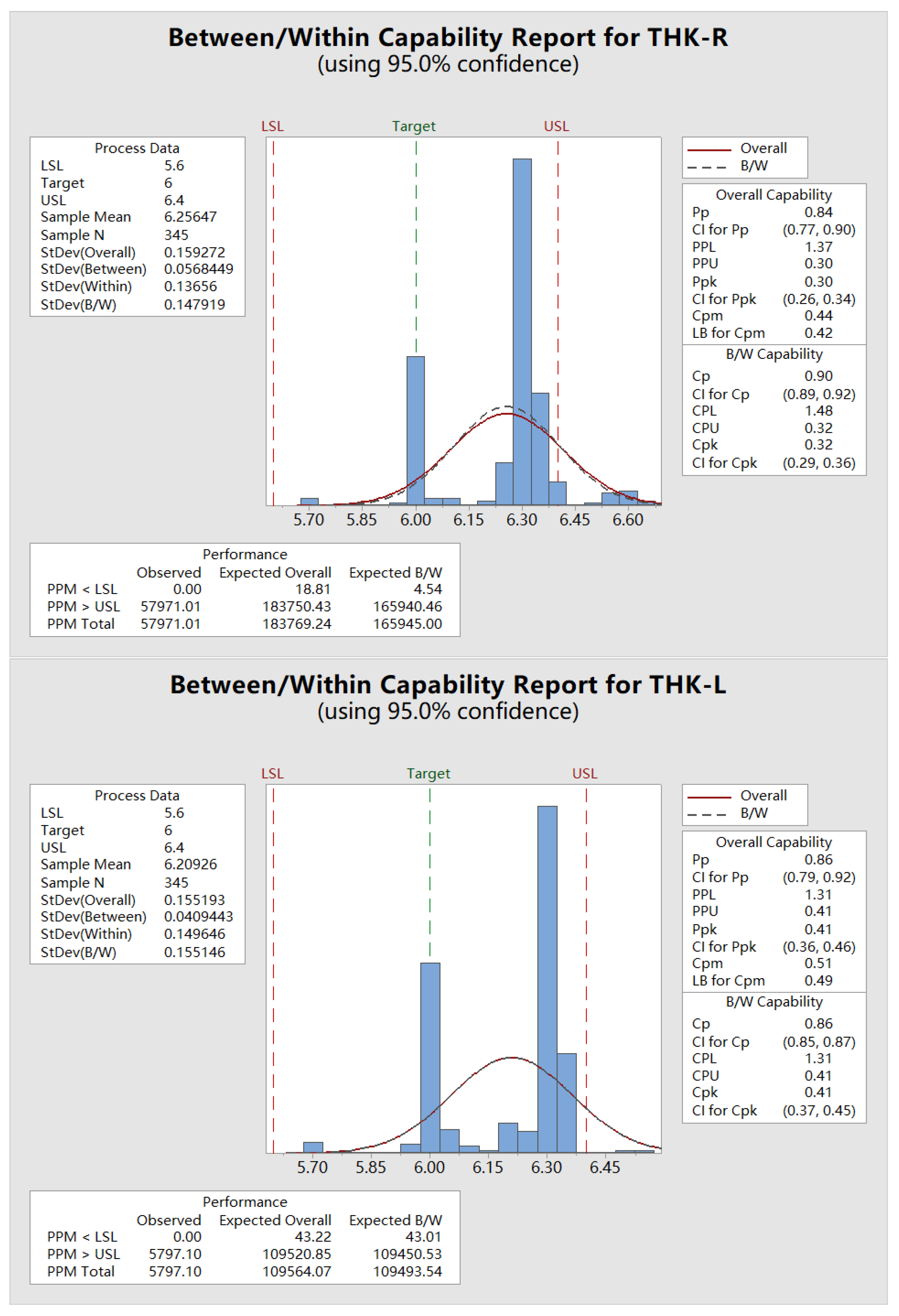
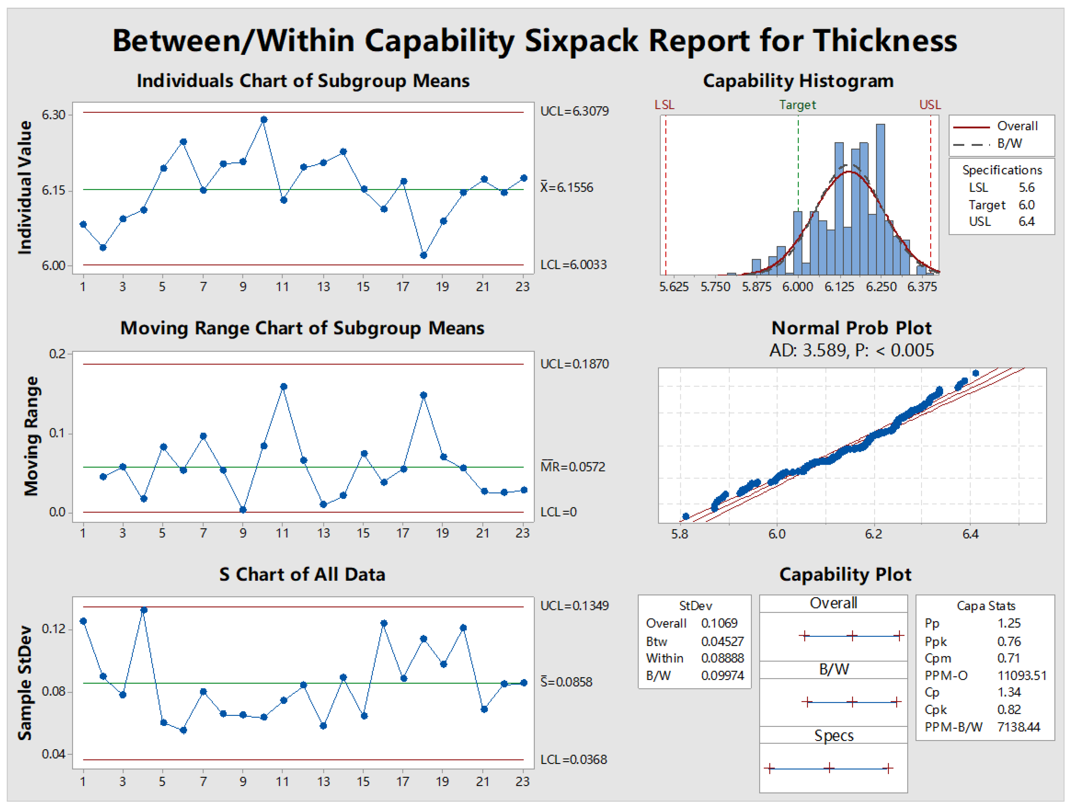
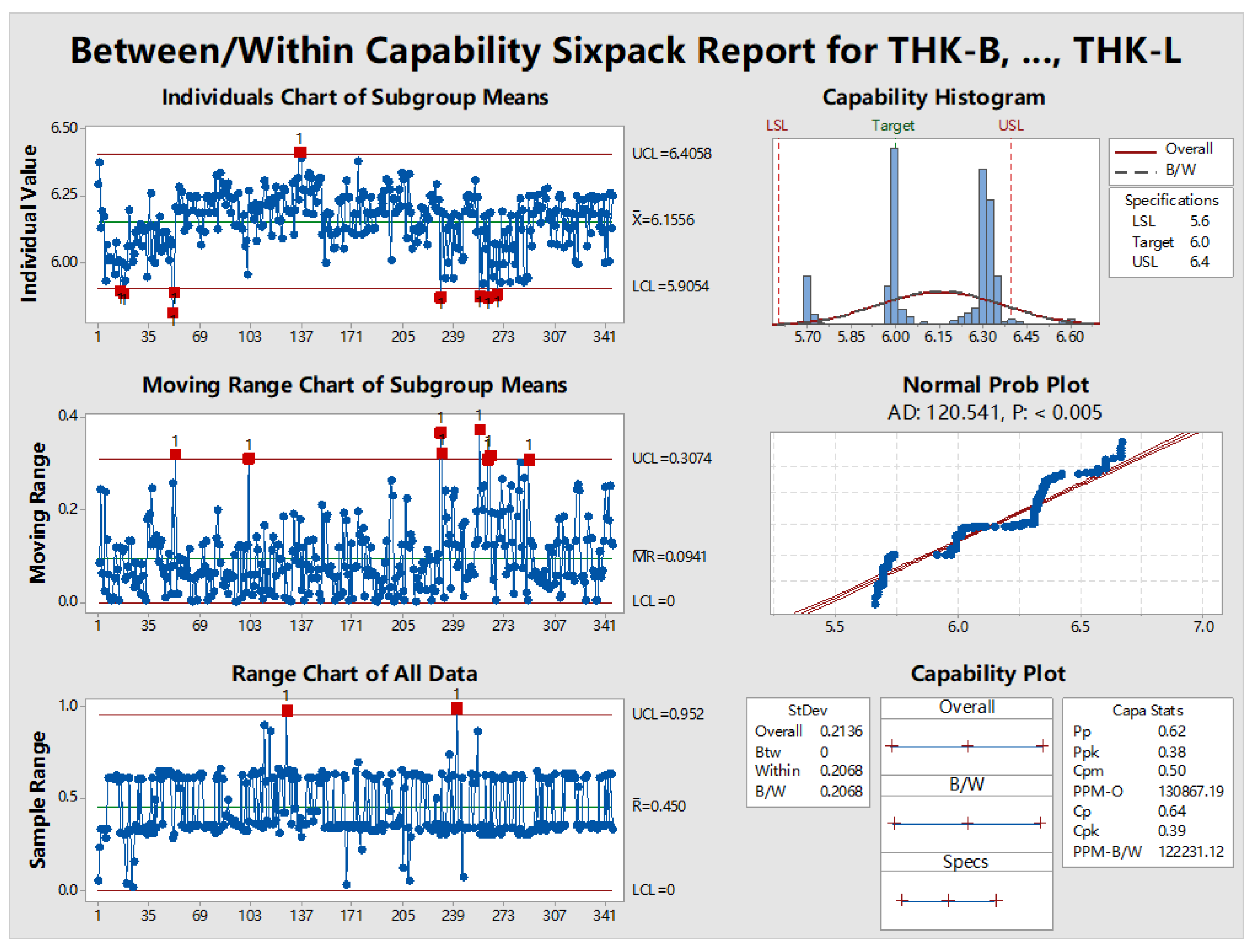
3.2. Thickness of the GeO2-SiO2 Optical Film

Figure 4 shows the thickness maps and histograms for the 345 wafers with the specification limits and targets for THK-B, THK-C, THK-T, THK-R and THK-L. The lower specification limit for the thickness was set at 5.6 μM. The upper specification limit was set at 6.4 μM and the thickness target was set at 6 μM. The data in Figure 4 does not have a normal distribution and there is an obvious divergence in the thickness of the 345 wafers. The thickness at points THK-B, THK-T, THK-R and THK-L was mainly distributed around 6.3 μM, while the thickness at THK-C was distributed around 6.0 μM. This is because the wafer was warped, resulting in a PECVD electrode gap between the showerhead reactor and the wafer. Wafer warpage is caused by insufficient cladding being deposited and annealed at 1100 °C, which is difficult to control.
As shown in Figure 4, the Cp for THK-C, THK-T, THK-R and THK-L was greater than 0.83 and less than 1.00, while the Cp for THK-B was less than 0.83. According to SPC theory, when the Cp is less than 0.83, the process capability is in trouble. The thickness distribution at the five points on each wafer was not uniform, especially at point B. The reason for this was because the gas flow was not uniform.
Figure 5 shows the thickness RI between/within capability sixpack report for the 23 lots and Figure 6 shows the RI between/within capability sixpack report for the 345 wafers. For the data in Figure 5 and Figure 6, p (the probability value test) was less than 0.05. This means that the thickness of the 23 lots or 345 wafers did not have a normal distribution because of the wafer warpage. However, the average thickness of the silica optical film per wafer was higher than the thickness target of 6.0 μM. As shown in Figure 5, the Cp for the 23 lots exceeded 1.33, while the Cpk for the 23 lots was below 1.33. This means that the lot fabrication capability for thickness was under control, but that the mean thickness was higher than the thickness target. The gap between the electrode and the wafer needed to be adjusted. In Figure 6, the Cp/Cpk for the 345 wafers was lower than 0.83, indicating that the process needed improvement.
In this case, there was no one-to-one mapping between the PLC process capability and the thickness of the lots and of the wafers overall. According to Figure 5 and Figure 6, the thickness at the five points on the wafer surface was uneven. In Figure 6, the tests for specific causes were set to “six points in a row, all increasing or all decreasing”. When the number of wafers exceeded 256 [256 pcs /15 (pcs/lot) = 17 days], the thickness value was lower than the LCL (lower control limit). In other words, after 17 days, the gap between the electrode and the wafer needed to be adjusted.

3.3. Process Control Strategy

Lot fabrication stability is a key factor in defining the usability of various materials, environments and technologies for fabrication processes. For the PLC process capability analysis conducted in Section 3.1 and Section 3.2, the optical waveguide specifications were determined according to variations in the fabrication process and, in theory, they obeyed a one-dimensional normal distribution. Unfortunately, there were many factors that were not adequately controlled. This means that the specific causes of variation had not been identified and eliminated, such as ambient temperature and relative humidity. According to Section 3.1 and Section 3.2, if the process parameters of the PLC remained unchanged for a long time, the RI and thickness of the optical film wafers would move beyond their designated range. In this PLC production line, the GeH4 (combined with 95% H2) flow needed to be adjusted to stabilize the RI of the optical film after every 8 lots (or 8 days) and the electrode and wafer gap needed to be adjusted to stabilize the THK of the optical film every 17 lots (or 17 days).

4. Conclusions

Silica optical film specifications are determined on the basis of variations in the fabrication process. In this study, we have analyzed the mapping between the PLC process capability and the RI and thickness of lots of silica optical film wafers. In addition to internal factors, there are key external factors that need to be taken into consideration during the PLC process, such as temperature, relative humidity, process variation and machine aging. Statistical process control (SPC) can be used during the process to analyze the process capability and the lot fabrication stability, enabling real-time decisions to be made regarding whether to improve the fabrication process. Here, for instance, it was found that, on the studied PLC product line, the GeH4 (combined with 95% H2) flow needed to be adjusted to stabilize the RI of the optical film after every 8 lots, while the electrode and wafer gap needed to be adjusted to stabilize the THK of the optical film after every 17 Lots.

Author Contributions

Conceptualization, Y.Z. and J.Z.; Methodology, Y.Z.; Validation, Y.Z.; Formal analysis, Y.Z. and P.G.; Investigation, Y.Z. and P.G.; Resources, Y.Z. and J.Z.; Writing—original draft preparation, P.G. and Z.X.; Writing—review and editing, P.G. and Y.Z.; Visualization, B.C.; Supervision, J.D.; Project administration, Y.Z. and J.D.; Funding acquisition, Y.Z. and J.D.

Funding

This research was funded by the National Natural Science Foundation of China (51475479), the National Key Research and Development Program of China (2017YFB1104800), the Key Research and Development Program of Hunan Province, China (2016GK2098), the State Key Laboratory of High Performance Complex Manufacturing, Central South University (ZZYJKT2017-07), the Key Laboratory for Precision & Non-traditional Machining of Ministry of Education, Dalian University of Technology (JMTZ201804).

Conflicts of Interest

The authors declare no competing financial interests.

References

  1. Choe, J.S.; Ko, H.; Choi, B.S.; Kim, K.J.; Youn, C.J. Silica planar lightwave circuit based integrated 1×4 polarization beam splitter module for three-space BB84 quantum key distribution. IEEE Photonics J. 2018, 10, 7600108. [Google Scholar] [CrossRef]
  2. Fujisawa, T.; Yamashita, Y.; Sakamoto, T.; Matsui, T.; Tsujikawa, K.; Nakajima, K.; Saitoh, K. Scrambling-type three-mode PLC Multiplexer based on cascaded Y-branch waveguide with integrated mode rotator. J. Lighwave Technol. 2018, 36, 1985–1992. [Google Scholar] [CrossRef]
  3. Himeno, A.; Kato, K.; Miya, T. Silica-based planar lightwave circuits. IEEE J. Sel. Top. Quantum Electron. 1998, 4, 913–924. [Google Scholar] [CrossRef]
  4. Doerr, C.R.; Okamoto, K. Advances in silica planar lightwave circuits. J. Lighwave Technol. 2006, 24, 4763–4789. [Google Scholar] [CrossRef]
  5. Watanabe, K.; Hashizume, Y.; Nasu, Y.; Kohtoku, M.; Itoh, M.; Inoue, Y. Ultralow power consumption silica-based PLC-VOA/switches. J. Lighwave Technol. 2008, 26, 2235–2244. [Google Scholar] [CrossRef]
  6. Dai, D.X. Subwavelength silica-based optical waveguide with a multilayered buffer for sharp bending. J. Lighwave Technol. 2009, 27, 2489–2499. [Google Scholar]
  7. Parks, J.W.; Wall, T.A.; Cai, H.; Hawkins, A.R.; Schmidt, H. Enhancement of ARROW photonic device performance via thermal annealing of PECVD-based SiO2 waveguides. IEEE J. Sel. Top. Quantum Electron. 2016, 22, 249–254. [Google Scholar] [CrossRef] [PubMed]
  8. Kim, Y.; Cho, S.; Seo, Y.; Yoon, H.; Im, Y.; Suh, S.; Yoon, D. Refractive index control of core layer using PECVD and FHD for Silica optical waveguide. Surf. Coat. Technol. 2003, 171, 34–38. [Google Scholar] [CrossRef]
  9. Liang, H.; Gordon, R.G. Atmospheric pressure chemical vapor deposition of transparent conducting films of fluorine doped zinc oxide and their application to amorphous silicon solar cells. J. Mater. Sci. 2010, 42, 6388–6399. [Google Scholar] [CrossRef]
  10. Shareef, I.A.; Rubloff, G.W.; Anderle, M.; Gill, W.N.; Cotte, J.; Kim, D.H. Subatmospheric chemical vapor deposition ozone/TEOS process for SiO2 trench filling. J. Vac. Sci. Technol. 1995, 13, 1888–1892. [Google Scholar] [CrossRef]
  11. Zhang, J.; Ren, Z.; Liang, R.; Sui, Y.; Liu, W. Planar optical waveguide thin films grown by microwave ECR PECVD. Surf. Coat. Technol. 2000, 131, 116–120. [Google Scholar] [CrossRef]
  12. Kilian, A.; Kirchof, J.; Przyrembel, G.; Wischmann, W. Birefringence free planar optical waveguide made by flame hydrolysis deposition (FHD) through tailoring of the overcladding. J. Lighwave Techol. 2000, 18, 193–198. [Google Scholar] [CrossRef]
  13. Enami, Y.; Derose, C.T.; Mathine, D.; Loychik, C.; Greenlee, C.; Norwood, R.A.; Kim, T.D.; Luo, J.; Tian, Y.; Jen, A.K.-Y.; et al. Hybrid polymer/sol-gel waveguide modulators with exceptionally large electro-optic coefficients. Nat. Photonics 2007, 1, 180–185. [Google Scholar] [CrossRef]
  14. Kim, Y.T.; Kim, D.S.; Yoon, D.H. PECVD SiO2 and SiON films dependent on the RF bias power for low-loss silica waveguide. Thin Solid Films 2005, 475, 271–274. [Google Scholar] [CrossRef]
  15. Bellman, R.A.; Bourdon, G.; Alibert, G.; Beguin, A.; Guiot, E.; Simpson, L.B.; Lehuede, P.; Guiziou, L.; LeGuen, E. Ultrlow loss high delta silica germania planar waveguides. J. Electrochem. Soc. 2004, 151, G541–G547. [Google Scholar] [CrossRef]
  16. Oakland, J.S. Statistical Process Control; Elsevier Ltd.: Oxford, UK, 2007. [Google Scholar]
Figure 1. Refractive index (RI) maps and histograms for the 345 wafers with their specification limits and target for RI-B, RI-C, RI-T, RI-R and RI-L. LSL = 1.4620, USL = 1.4634 and the target = 1.4627.
Applsci 09 00785 g001aApplsci 09 00785 g001bApplsci 09 00785 g001c
Figure 2. RI between/within capability sixpack report results for the 23 lots.
Applsci 09 00785 g002
Figure 3. RI between/within capability sixpack report results for the 345 wafers.
Applsci 09 00785 g003
Figure 4. Thickness histograms for the 345 wafers for THK-B, THK-C, THK-T, THK-R and THK-L. LSL = 5.6 μM, USL = 6.4 μM and the target = 6.0 μM.
Applsci 09 00785 g004aApplsci 09 00785 g004bApplsci 09 00785 g004c
Figure 5. Thickness Between/Within Capability Sixpack for the 23 lots.
Applsci 09 00785 g005
Figure 6. Thickness between/within capability sixpack report for the 345 wafers.
Applsci 09 00785 g006

