Abstract
Besides the application of the photonic crystal for the photodetector in the visible range, the infrared devices proposed with subwavelength structure are numerically and experimentally investigated thoroughly for infrared radiation sensing in this research. Several complementary metal oxide semiconductor (CMOS) compatible thermopiles with subwavelength structure (SWS) are proposed and simulated by the FDTD method. The proposed thermopiles are fabricated by the 0.35 μm 2P4M CMOS-MEMS process in TSMC (Taiwan Semiconductor Manufacturing Company). The measurement and simulation results show that the response of these devices with SWS is higher than for those without SWS. The trend of the measurement results is consistent with that of the simulation results. Obviously, the absorption efficiency of the CMOS compatible thermopile can be enhanced when the subwavelength structure exists.
1. Introduction
Based on the photonic crystal (PhC), it is proved to successful in the efficient photon coupling into photodetectors when the PhC structure is employed [1]. Besides the visible range, thermopiles as the infrared sensor converting thermal energy into electrical energy can sense heat radiation and generate an output voltage proportional to a local temperature difference or temperature gradient [2]. Thermopiles working as infrared sensors can be used in many applications, such as remote temperature sensing [2,3,4,5] and non-dispersive infrared sensing (NDIR) gas detection [6]. In recent decades, with the development of micro-electromechanical systems (MEMS) technology, the problem of mass production of thermopile IR sensors has been effectively solved, and the manufacturing cost has been greatly reduced [3,4]. MEMS technology can be a goal of continuous integration, miniaturization, extended functionality, lowering cost, and improved performance and reliability. For the requirements of integration, the monolithic complementary-metal-oxide-semiconductor (CMOS) MEMS integration that integrates MEMS structures with integrated circuits (IC) on a single CMOS substrate is developed [7]. The digital micro-mirror device (DMD) manufactured by Texas Instruments (TI) is a well-known commercial monolithic CMOS-MEMS device [8,9].
Some researchers focus on the enhancement of infrared emitters or absorbers by adding specifically artificial structures. A unique thermally stimulated mid-infrared source emitting radiation within a narrow range of wavelengths is experimentally and theoretically investigated [10]. Here, the periodicity of a metal coated silicon–air photonic crystal etched into the emitter surface determines the emission wavelength. Wavelength-selective uncooled IR sensors using square lattice two-dimensional plasmonic absorbers are investigated [11]. The results show that selective enhancement of the responsivity is achieved, and for the detection wavelength the triangular lattice case is shorter than the square lattice case. A 2D photonic crystal is first proposed to enhance the infrared absorption efficiency of thermopiles [12]. The experimental results show that the thermopiles with 2D microstructures have a significantly higher response than those without the photonic crystal. To meet the commercial batch production, the thermopile with photonic crystal is fabricated by the CMOS MEMS process.
Beyond the development of optimized structured absorbers for CMOS infrared detectors empirically, it was firstly proposed with theoretical analysis and investigation with experiments thoroughly. In this study, various CMOS compatible thermopiles with subwavelength structures are fabricated in the standard 0.35 m CMOS-MEMS, which are numerically and experimentally investigated and reach agreement with response curves. The various subwavelength structures (SWSs) of photonic devices are analyzed by the finite-difference time-domain (FDTD) [13,14] method. Then, the thermopile with subwavelength structure (SWS) [15] is fabricated by the 0.35 μm 2P4M CMOS-MEMS process. Finally, we discuss the results of structural measurement and summarize in the conclusion. The measurement and simulation results show that the CMOS compatible thermopiles with SWS are higher than the one without SWS.
2. Research Preliminary
Based on the cantilever beam structure floating over an etched silicon cavity, the properties of SWS were investigated and measured for the properties of infrared absorption. The working principle of infrared absorption on the front-side of a thermopile is depicted in Figure 1 [16], and the dynamic thermal behavior is governed by the heat equation including the exchange of thermal radiation between the infrared source and sensor, and solid conduction and convective conduction, which are described in Equation (1). The spectral absorption of thermal radiation for SWS is more important to be highlighted as R(λ). The absorption of the rest area of cantilever beam structure is denoted as Rm. The temperature of hot junction, ambient environment and radiation source are denoted as , and , respectively. is used to describe the geometrical factor of the light path between the radiation source and sensor. and are the emissivity of radiation source and the sensor, respectively. H is the heat capacitance of thermopile membrane and , are the active area and the rest area of cantilever beam structure, respectively. h is the convective heat transfer coefficient and is the total area of cantilever beam structure.
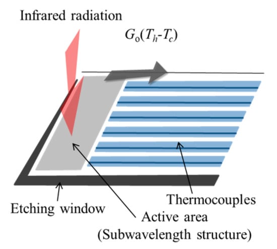
Figure 1.
Schematic diagram of heat conduction for the CMOS thermal sensor.
Without an external heat source , Equation (1) can be simplified and manipulated as Equation (2) and the infrared radiation exchange plays the major role of heat source in the heat equation. ε is the emissivity of absorption area and plays the major role of the infrared absorption for our proposed SWSs. is the total thermal conductance including the solid and heat convection, which conduct the heat to the environment at the ambient temperaturei.e., =+.
The response time and bandwidth of frequency response, for thermal sensor are determined by H and G, which can be estimated and measured. The frequency response curve through the modulation of infrared radiation with mechanical chopper is preceded and then it can conduct the thermal time constant, which is expressed as the following Equation (3).
3. Simulation Results and Discussion
To explore the effect of the SWSs for the CMOS thermal sensor, the rectangular hole and circular hole structural parameters of the SWS CMOS compatible thermopile are analyzed by the FDTD method and compared with the one without SWS. Figure 2 shows the schematic diagram of lightwave propagation through a CMOS compatible thermopile with SWS simulated by the FDTD method. Here, and are the refractive indices of the incident medium and SiO2, respectively. In this study, we take = 1 for air and = 1.42 for SiO2 FDTD simulation, absorbing boundary conditions are required to truncate the computational domain without reflection. A perfect matched layer (PML) is a useful method to decrease this error induced form the boundary situation [17,18], so we use the PML boundary to be the simulated area. To explore the effect of incident infrared radiation in the active area, the absorption, transmittance, and reflectance detectors are used. Figure 3 shows the schematic top-view of the rectangular-hole and circular-hole patterns for the SWS, respectively. For the rectangular-hole type (RHT) cases, the length is taken as 15 μm, the width is considered as 3, 3.5 and 4 μm, and the spacing is the same as the width. For the cylindrical-hole type (CHT) cases, the diameter is considered as 3, 3.5 and 4 μm and the spacing is the same as the diameter.

Figure 2.
Schematic diagram of light-wave propagation through a CMOS compatible thermopile with subwavelength structure (SWS) simulated by the FDTD method.
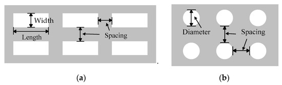
Figure 3.
Schematic top-view of the (a) rectangular-hole and (b) cylindrical-hole patterns for the SWS.
Figure 4 shows the simulation results of the normalized absorption difference with the target temperature for the thermopiles without the SWS, with the RHT SWS, and with the CHT SWS, respectively. The normalization for the data to be analyzed in the following is applied while the maximum of absorption curve is adopted as the 100%. One can see that the maximum is the result of the case of RHT thermopile with the SWS width 3.5 μm at target temperature 75 °C and those results with SWS are obviously better than those without SWS in Figure 4. For the CHT cases, the case of the diameter of 3 μm is higher than the other cases. The results of the RHT thermopile and CHT thermopile are higher than those without the SWS.
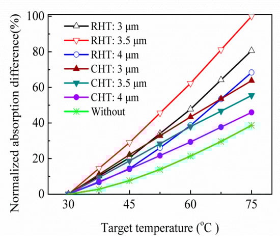
Figure 4.
Simulation results of the normalized absorption difference with the target temperature for the thermopiles for the thermopiles with various SWS.
4. Experimental Results and Discussion
Thermopile sensors are designed and fabricated by using the TSMC 0.35 µm 2P4M CMOS-MEMS process, which is achieved after a series of anisotropic etching. As a thermopile is a device that uses a local temperature difference to measure thermal radiation, it is susceptible to environmental conditions. To avoid this problem, we configured several proposed thermopiles with various SWSs and a thermopile without an SWS in the same chip. Figure 5 shows the schematic diagram of the structure of TSMC 0.35 µm 2P4M CMOS MEMS. The standard CMOS process in TSMC fabricates the array of thermocouples with CMOS materials of polysilicon and aluminum as in step 1.
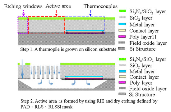
Figure 5.
Schematic diagram of the structure of TSMC 0.35 µm 2P4M CMOS-MEMS process.
In step 2, the etching windows and active area are formed by some specific MEMS processes. There structures are fabricated with RLS and RLSSI processes which etch the Si3N4/SiO2 layers and silicon substrate subsequently. The patterns of the SWS are formed in the RLS process with RIE etching of the Si3N4/SiO2 layers on the active area. By using the RLSSI process, the RIE etching of silicon substrate is proceeded under the membrane. Therefore, the sensing area is floated and filled with arrays of etching hole as the periodic refractive index waveguide. The silicon substrate beneath the cantilever beam is removed and only a thin structure layer with 7 μm thickness is left on top. The structure of the thermocouples is designed with a strip of n-poly 20 μm width and a length of 200 μm. An aluminum wire with a width of 0.5 μm was deposited on top of the n-type polysilicon. Finally, the thin cantilever beam was floating upon the etched cavity with a poor thermal conduction, which served as a sensing structure and a good platform for investigation and analysis of SWSs. To show the effect of the SWSs for the CMOS compatible thermopile, the thermopile without SWS was also simulated and fabricated.
Figure 6a,b shows SEM images of a CMOS compatible thermopile, which can be compared to Figure 1 and Figure 5. The active area filled with IPC is verified to suspend over a cavity of silicon substrate and the cantilever beam structure is well built under the processes. The thermocouples are patterned and embedded between the passivation oxide layers. Figure 6a,b shows the SEM of (a) RHT and (b) CHT subwavelength structures for the CMOS compatible thermopile. One can see that the structures of SWS are well fabricated for thermopile devices and both are successfully fabricated by the CMOS-MEMS process. It is worth noting that holes of RHT and CHT subwavelength structures are well defined, as in our design. The size of the design, 3 × 15 μm for RHT after dry etching of active area deviated to 3.27 × 15.15 μm in Figure 6a, and the diameter of design at 3.5 μm for CHT after dry etching of active area deviated to an average of 3.82 μm in Figure 6b. The cause of deviation may come from the over-etching of the undercut of the structure and error of tilt angle of SEM measurement.
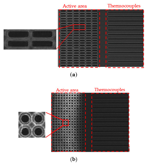
Figure 6.
SEM image of the CMOS compatible thermopile with (a) rectangular-hole type (RHT) and (b) circular-hole type (CHT) subwavelength structures.
To investigate the absorption efficiency between our infrared thermopiles with SWS, thorough measurements for the output voltage of thermopiles with SWS were carried out. The setup of measurement was arranged as shown in Figure 7, consisting of a standard infrared radiation source and a modulated mechanical chopper system. The output signal of the thermopile is amplified with a chopper-amplifier AD8551 and the signal is delivered to a digital multi-meters (DMM). The infrared radiation source is placed 40 mm distance away from the sensor chip. The temperature of infrared radiation source is set to be between 30 °C and 75 °C at increments of 15 °C. In addition, to avoid interference from ambient light or other background signals, we set up a chopper before the sensor chip and a 5–14 μm infrared filter.
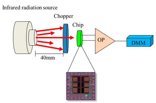
Figure 7.
Setup of the experimental measurement framework for the thermopiles.
To investigate the bandwidth of proposed thermopile, the measurement of frequency response was built and is shown in the Figure 8. The frequency ranged from 1–150 Hz to investigate the bandwidth of the frequency response and the range was much higher than the bandwidth of the proposed thermopile. The results of the infrared modulation measurement for thermal time constants of sensors under various conditions are shown in Table 1. The time constant was about 5 ms and the corresponding bandwidth was 32 Hz, which has proved to be practical for the applications of infrared thermometer and thermal imagery.
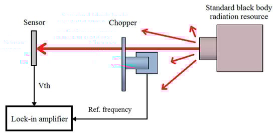
Figure 8.
Setup of the frequency response measurement for the thermopiles.

Table 1.
Frequency response measurement with infrared radiation.
The prototypes for the thermopile without the SWS, the RHT thermopile with the SWS width of 3 or 3.5 μm, and the CHT thermopile with the SWS diameter of 3 or 3.5 μm, were measured and the results are shown in Figure 9. Here, the output voltage difference is the difference between the thermopile with SWS and the one without SWS. It can be seen that the maximum is the result for the case of the RHT thermopile with an SWS width of 3.5 μm at a target temperature of 75 °C. The best case of the measurement is the same as the one of the simulation and is also the RHT case for the SWS width of 3.5 μm, that is, the maximum is the result of the RHT thermopile with the SWS width 3.5 μm at a target temperature of 75 °C. For the CHT thermopiles, the case of the SWS diameter 3 μm was also higher than the other cases. Comparing Figure 9 with Figure 4, it can be seen that the normalized experiment results are highly consistent with the normalized simulation results.
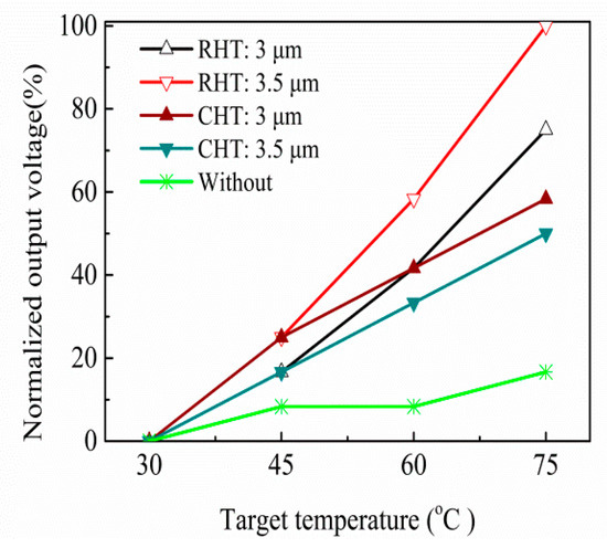
Figure 9.
Normalized output voltage difference with the target temperature for the thermopiles with various SWS.
5. Conclusions
In this study, we numerically and experimentally investigated the thermopiles with SWS. Several thermopiles with RHT SWS or CHT SWS were simulated by the FDTD method. Based on the considerations of commercial batch production and mechatronics, the fabrication for the proposed thermopiles uses a compatible to the CMOS process. To avoid the impact of differences in measured environmental conditions, those proposed thermopiles were fabricated in the same chip and were measured at the same time. Among those cases, the simulation results show that the case with the RHT thermopile and an SWS width of 3.5 μm has the largest infrared absorption. According to the measurement results, the best sample is also the RHT thermopile with an SWS width of 3.5 μm. The measurement and simulation results show that the FDTD simulation method is effective for this type of thermopile and the response of these devices with SWS is higher than thermopile without SWS.
Author Contributions
All the authors participated in the design of experiments, analysis of data and results, and writing of the paper.
Funding
This research received no external funding.
Conflicts of Interest
The authors declare no conflict of interest.
References
- Yang, J.K.; Seo, M.K.; Hwang, I.K.; Kim, S.B.; Lee, Y.H. Polarization-selective resonant photonic crystal photodetector. Appl. Phys. Lett. 2008, 93, 211103. [Google Scholar] [CrossRef]
- Rogalski, A. Infrared Detectors; CRC Press: Boca Raton, FL, USA, 2010. [Google Scholar]
- Graf, A.; Arndt, M.; Sauer, M.; Gerlach, G. Review of micromachined thermopiles for infrared detection. Meas. Sci. Technol. 2007, 18, R59. [Google Scholar] [CrossRef]
- Xu, D.; Wang, Y.; Xiong, B.; Li, T. MEMS-based thermoelectric infrared sensors: A review. Front. Mech. Eng. 2017, 12, 557–566. [Google Scholar] [CrossRef]
- Van Herwaarden, A.W. Overview of calorimeter chips for various applications. Thermochim. Acta 2005, 432, 192–201. [Google Scholar] [CrossRef]
- Rubio, R.; Santander, J.; Fonseca, L.; Sabate, N.; Gracia, I.; Cane, C.; Marco, S. Non-selective NDIR array for gas detection. Sens. Actuators B Chem. 2007, 127, 69–73. [Google Scholar] [CrossRef]
- Qu, H. CMOS MEMS fabrication technologies and devices. Micromachines 2016, 7, 14. [Google Scholar] [CrossRef] [PubMed]
- Hornbeck, L.J. The DMD TM projection display chip: A MEMS-based technology. Mrs Bull. 2011, 26, 325–327. [Google Scholar] [CrossRef]
- Zhou, G.; Lee, C. Optical MEMS, Nanophotonics, and Their Applications; CRC Press: Boca Raton, FL, USA, 2017. [Google Scholar]
- Ryu, H.Y.; Hwang, J.K.; Lee, Y.J.; Lee, Y.H. Enhancement of light extraction from two-dimensional photonic crystal slab structures. IEEE J. Sel. Top. Quantum Electron. 2002, 8, 231–237. [Google Scholar]
- Takagawa, Y.; Ogawa, S.; Kimata, M. Detection Wavelength Control of Uncooled Infrared Sensors Using Two-Dimensional Lattice Plasmonic Absorbers. Sensors 2015, 15, 13660–13669. [Google Scholar] [CrossRef] [PubMed]
- Hsu, P.H.; Tsai, M.H.; Shen, C.H.; Chen, S.J. Investigation of thermal type microsensor with infrared photonic crystal. In Proceedings of the 2010 IEEE SENSORS, Kona, HI, USA, 1–4 November 2010; pp. 829–832. [Google Scholar]
- Zhou, J.; Huang, L.; Fu, Z.; Sun, F.; Tian, H. Multiplexed simultaneous high sensitivity sensors with high-order mode based on the integration of photonic crystal 1 × 3 beam splitter and three different single-slot PCNCs. Sensors 2016, 16, 1050. [Google Scholar] [CrossRef] [PubMed]
- Hong, J.S.; Cheng, W.M.; Yang, M.C.; Shiu, R.C.; Lan, Y.C.; Chen, K.R. Enhancing Efficiency of Electromagnetic Simulation in Time Domain with Transformation Optics. Appl. Sci. 2018, 8, 1133. [Google Scholar] [CrossRef]
- Lee, T.X.; Chou, C.C. Scale-dependent light scattering analysis of textured structures on LED light extraction enhancement using hybrid full-wave finite-difference time-domain and ray-tracing methods. Energies 2017, 10, 424. [Google Scholar] [CrossRef]
- Schneeberger, N.; Paul, O.; Baltes, H. Optimized structured absorbers for CMOS infrared detectors. In Proceedings of the International Solid-State Sensors and Actuators Conference-TRANSDUCERS’95, Stockholm, Sweden, 25–29 June 1995; Volume 2, pp. 648–651. [Google Scholar]
- Yee, K. Numerical solution of initial boundary value problems involving Maxwell’s equations in isotropic media. IEEE Trans. Antennas Propag. 1966, 14, 302–307. [Google Scholar]
- Taflove, A.; Hagness, S.C. Computational Electrodynamics: The Finite-Difference Time-Domain Method; Artech House: Norwood, MA, USA, 2005. [Google Scholar]


© 2019 by the authors. Licensee MDPI, Basel, Switzerland. This article is an open access article distributed under the terms and conditions of the Creative Commons Attribution (CC BY) license (http://creativecommons.org/licenses/by/4.0/).