1. Introduction
The same as the electrical current diode concept, thermal rectification is a phenomenon in which heat travels in one preferred direction with high thermal conductivity and in the opposite direction with low conductivity [
1]. This concept has been known as the basis for thermal diodes and later thermal transistors and thermal logic circuits. A self-driven thermal computer is the final goal of this study [
2]. On the other hand, thermal diodes or switches are the key components for solving complicated thermal management problems, especially as the size of the device decreases to nanometers [
3]. Historically, the first experimental observation of thermal rectification was made by Starr in 1936 [
4]. After that, a number of studies were carried out for bulk thermal rectifiers and several theoretical models have been proposed to understand the mechanisms. A good review can be found in [
5] on this topic. The involved physical mechanisms for thermal rectification include asymmetric roughness at the contact surface, a thermal potential barrier between material contacts, different temperature dependence of thermal conductivity and so on [
5].
In recent years, the research focus of thermal rectification has been changed to nanomaterials along with the greatly increased interest in micro/nanoelectronic cooling and quantum thermal systems. Moreover, as the dimension scales down, new physical mechanisms need to be revealed to understand the thermal rectification at the nanoscale. On this subject, many molecular dynamics (MD) simulations and much theoretical work have been published in the past decade. Some normally accepted mechanisms are addressed here. The first one is the overlap between the phonon spectra of two connecting materials or asymmetric nanostructures [
6,
7]. The phonon spectra overlap can be used to explain the thermal rectification across the interface between two dissimilar materials. The calculation of vibrational density of states (vDOS) indicates that the phonon spectra overlap varies by switching the direction of the temperature gradient. For nano-devices, the local phonon spectra depend on both the temperature and size of the material. Different phonon spectra overlaps may exist for a single-material device by changing the heat flux direction [
8]. The second one is the dependence of thermal conductivity on temperature and space, which is also one of the mechanisms to explain the thermal rectification in bulk materials. However, the origin of this asymmetric dependence of thermal conductivity is different between bulks and nanomaterials. For the bulk device with two dissimilar materials connecting at an interface, it is necessary to have different temperature-dependent thermal conductivities in each segment to result in thermal rectification, i.e., thermal conductivity in material A increases with increasing temperature while the thermal conductivity in material B has the opposite trend [
5]. For the nanomaterials, thermal conductivity is no longer a single-valued function of temperature. It depends on many factors, such as width, defect, surface roughness, etc. [
9,
10,
11,
12,
13]. For the nanomaterial with asymmetric geometric size or defects, the thermal conductivity is also a space-dependent function. In this case, thermal rectification occurs in a single nanomaterial by switching the direction of the temperature gradient. The third one is the local phonon edge scattering effect. For the nanomaterials, the mean free path of phonons could be comparable with the lateral size of the sample. Therefore, the phonon edge scattering becomes an important factor for the thermal conductivity. In an asymmetric nanomaterial with one narrow end and one wide end, the narrow end imposes a stronger edge scattering effect on the propagating phonon modes and this lateral confinement on phonons is temperature dependent due to the different phonon energy level. As a result, the thermal rectification will be triggered [
14]. The fourth one is the asymmetric scattering of ballistic phonons, which is easier to realize experimentally compared to the idealized one-dimensional chain approaches. For example, for a thin film with pyramidal inclusions (or some other asymmetric nanostructures), phonons emitted from the top contact are more likely to be transmitted, while phonons emitted from the bottom contact are more likely to be backscattered. This demonstrates the asymmetry of heat conduction in the devices [
15].
Here, we only mentioned several important physical mechanisms for nanomaterials, while a large number of MD simulations have been published, especially for the two-dimensional materials. By designing asymmetric thickness [
16], width [
17,
18,
19], strain [
20,
21], and defect [
22,
23] graphene structures in the simulation, thermal rectification could be realized.
Dames and Wu conducted a very complete and significant review of experimental demonstrations for thermal diodes, switches, and regulators, which covers the fields of heat conduction, convection, and radiation. After organizing and summarizing a wide variety of physical mechanisms, this review discusses the potential applications for the switchable and nonlinear heat transfer [
24].
On the other hand, experimental studies are quite scarce for thermal rectification at the nanoscale due to the challenge of manufacturing asymmetric nanostructures. Nevertheless, rapidly developing nanotechnology has enabled recent experimental advances to be made and provided valuable measurement data for MD simulation and theoretical analysis. The new nanotechnology and experimental skills discussed in this paper also provide clear guidance for the future development of efficient thermal rectifiers at the nanoscale.
2. Experimental Study
This section mainly introduces the recent experimental achievements in thermal rectification. The rapid advancement of nanofabrication, which has enabled the synthesis of nanostructures with a variety of materials, has been used in these studies. Significant thermal rectification phenomena have been observed, revealing different physical mechanisms.
2.1. Thermal Rectification at the Bimaterial Nanocontact Interface
Cao et al. studied the interface-induced thermal rectification in nanowires through experiments and molecular dynamics simulations [
25]. They built an organic/inorganic system consisting of silicon (Si) nanowires and polyamide (PA) nanofibers. The thermal conductivity was measured by a high heat flux resolution test platform [
26].
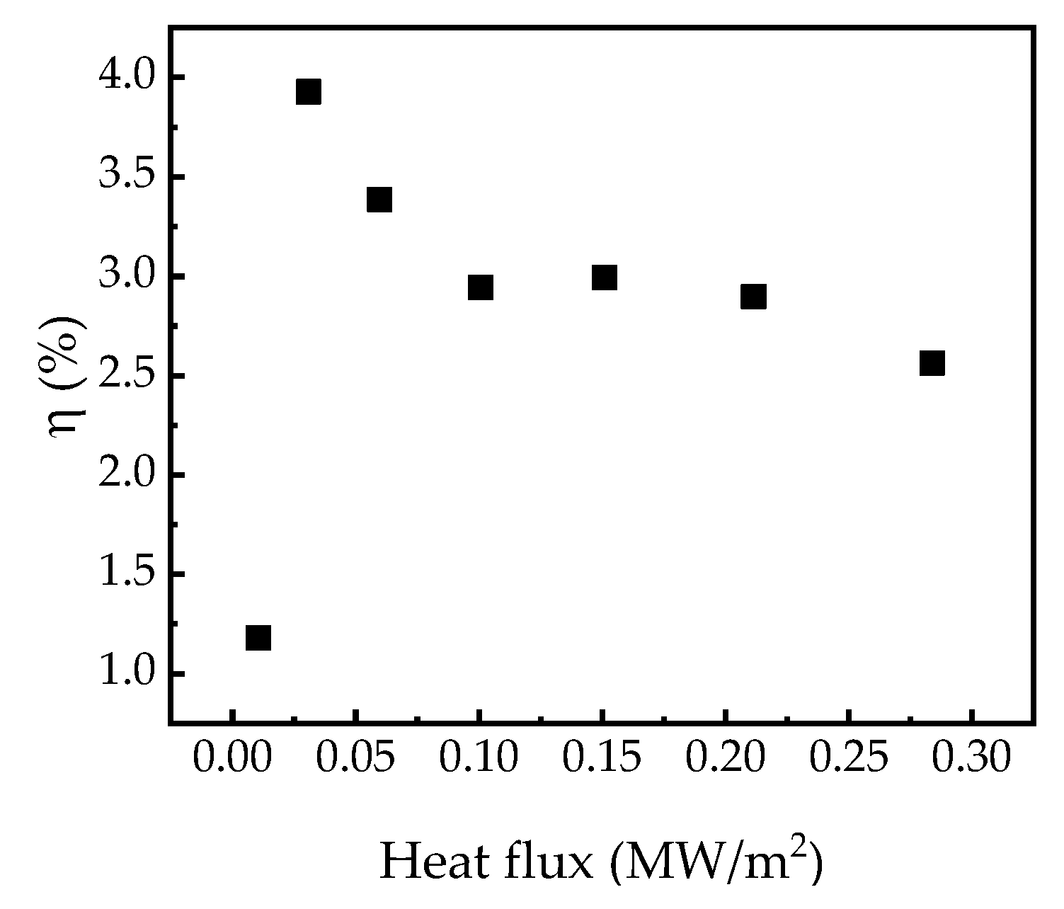
Figure 1 shows the change of the thermal rectification coefficient with respect to the heat flux at room temperature. Except for the first point in the figure, the thermal rectification coefficient equates to approximately 3%. The experimental results show that there is no significant correlation between the heat flux and the thermal rectification coefficient, which they believe is due to the low heat flux used in the experiment. However, molecular dynamics simulations show that high heat flux significantly affects the thermal rectification coefficient, but high heat flux could not be used in the experiment in order to avoid damage to the test samples. Molecular dynamics simulations were used to analyze the physical mechanisms of the thermal rectification effects, performed by the LAMMPS package [
27]. The simulation results show that the heat flux of Si-to-PA is always larger than that of PA-to-Si, which is consistent with the experimental observations. The result indicates that a strong edge effect exists in the nanowires, which reduces the amplitude of the phonon spectrum and moves the peak to a lower frequency region. It is a sign that the phonon localization occurs at the interface between PA and Si nanowires, resulting in a decrease of thermal conductivity. The thermal rectification effect at the PA/Si nanowire interface could be understood as the different degrees of phonon localization in different heat flux directions. In the process of using phonon spatial distribution to describe the degree of phonon localization, it was found that phonon localization only occurs at the interface. Moreover, in the heat flux direction from Si to PA, the phonon localization at the interface is smaller than that from PA to Si. The internal phonons have no obvious difference in two opposite directions.
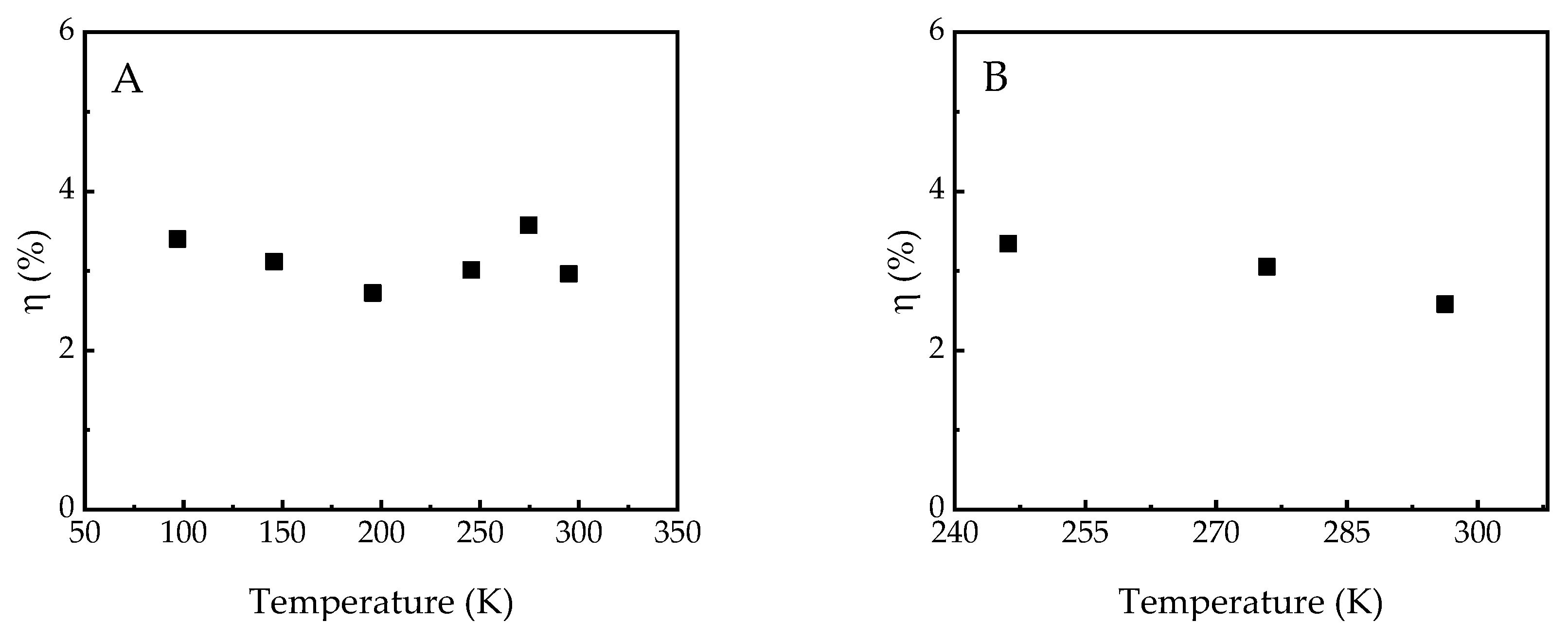
In order to further confirm the origin of this interface-induced thermal rectification effect, another kind of sample composed of PA and Si nanowires was experimentally tested. The contact area of the second kind of sample was much larger than that of the first kind, which means that the contact heat resistance could be smaller. However, the experimental results show that the thermal rectification coefficient was almost unchanged for these two samples, so there is no obvious correlation between the thermal rectification and contact area (
Figure 2).
It needs to be mentioned that the mechanism of thermal rectification at the nanocontact interface is different from the conventional model of bulk materials. In bulks, one important reason for the thermal rectification effect is the asymmetric temperature dependence of thermal conductivity. In the case of the Si-to-PA system, the thermal conductivity of polymers increases with increasing temperature, while the temperature dependence of thermal conductivity is opposite for Si. This indicates that the PA-to-Si heat flux direction has larger thermal conductivity, where PA is in the high temperature region and Si is in the low temperature region. On the other hand, the thermal rectification in the PA/Si nanowire structure is caused by the asymmetric temperature dependence of thermal resistance at the nanocontact interface.
2.2. Thermal Rectification of Asymmetric Nanotubes
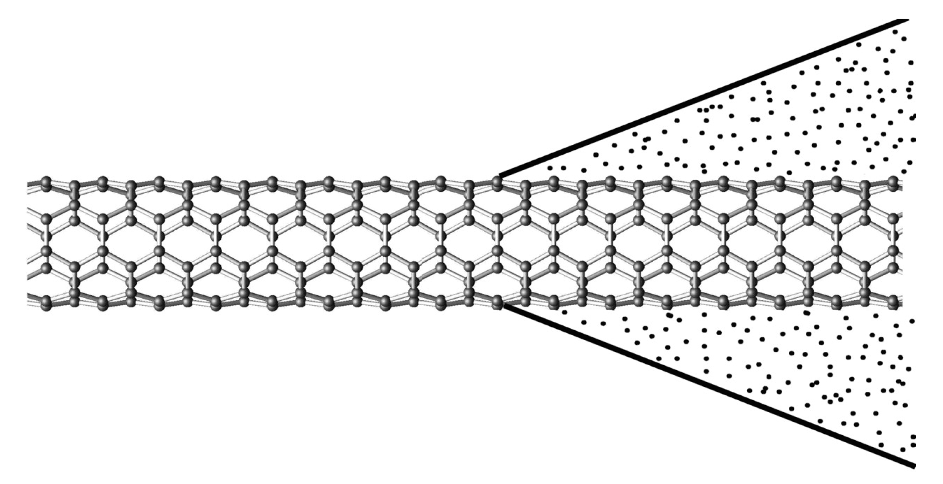
Chang et al. created a one-dimensional thermal rectifier by loading heavy molecules with non-uniform mass outside the carbon nanotubes (CNT) and boron nitride nanotubes (BNNT) [
28]. It was found that a larger heat flow occurs in the direction of lowering the mass density and the maximum rectification ratio reached 7%.
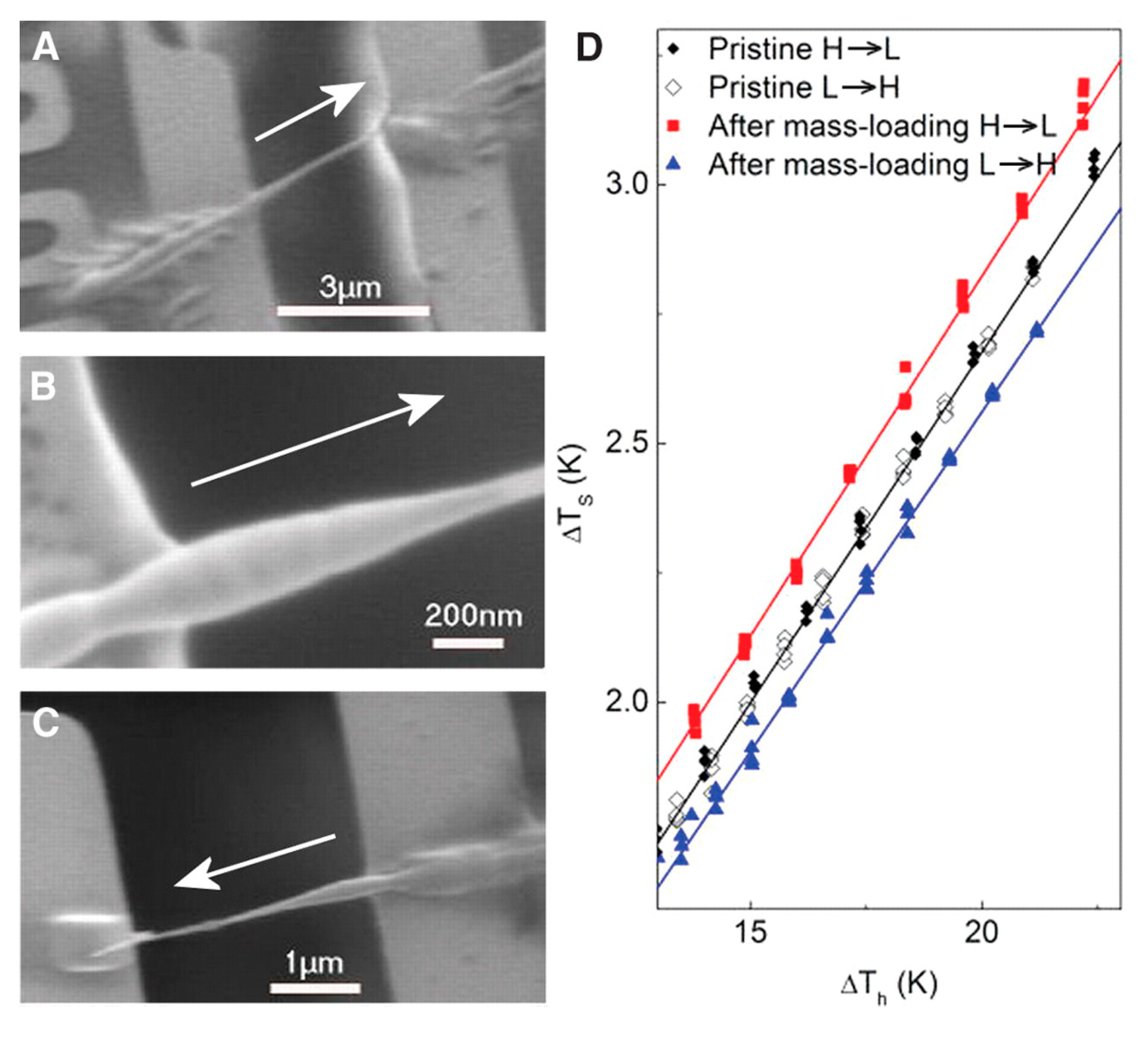
A customized microscale thermal measurement device was used to measure the thermal conductivity of the nanotube, driven by a piezoelectrical manipulator operating within a scanning electron microscope (SEM). In this micro-device, two symmetrically fabricated Pt thin film resistors were used as heater and temperature sensors, respectively. The nanotube was suspended between the heater and sensor pads. The thermal measurement was carried out in high-vacuum. The direction of heat flow can be simply changed by exchanging the role of heater and sensor in the experiment.
The original multi-walled BNNT was made by improving the fabrication method introduced in Ref. [
29], and the high-quality CNT was made by the conventional electric arc method introduced in Ref. [
30]. To achieve the thermal rectification effect, the asymmetry of the nanotube was achieved by depositing trimethyl-cyclopentadienyl platinum (C9H16Pt) at one end of the tube as shown in
Figure 3. Since the thermal conductivity of C9H16Pt was less than 1% of that of the nanotube, its direct contribution to the thermal conductivity could be ignored. The thermal conductivity of the same nanotube was measured in both heat flow directions. The experimental results show that the thermal conductivity is higher when heat flows from the high-mass end to the low-mass end (
Figure 4). As for CNT, a 2% thermal rectification coefficient was observed, and for BNNT, a 7.4% thermal rectification coefficient was observed.
In general, the asymmetric geometry can introduce asymmetric phonon scattering boundaries, which can possibly cause asymmetry in the heat transfer. However, following this mechanism, a higher thermal conductivity should be observed when heat flows from the narrow end to the wide end, which is contrary to the phenomenon observed in the experiment. Therefore, the asymmetric boundary is not the cause of the thermal rectification phenomenon. In fact, the sp2 bond in the nanotube is much stronger than the bond between the tube and the condensed C9H16Pt molecules. The phonons are confined inside the nanotube without propagating between CNT and C9H16Pt, so the thermal rectification is unaffected by the phonon scattering at asymmetric boundaries.
Theoretical studies have shown that stable solitons do exist in the nanotubes. Solitons are the nonperturbative solutions of the non-linear systems, which are localized particle-like entities that can collide with each other without changing shape. For a category of soliton models, the thermal rectification effect is a common phenomenon in the asymmetric structures. For instance, the Korteweg de Veries equation describes the relationship between the reflection magnitude and two different atomic masses. An important result of this equation is that in this mass-asymmetric system, heat is more easily transferred from the high-mass end to the low-mass end, which is consistent with the observed thermal rectification in the experiments. This model can be used to roughly estimate the thermal rectification effect; the corresponding thermal rectification coefficients for CNT and BNNT are around 5% and 7%, respectively. The theoretical calculation agrees well with the experimental results.
2.3. Thermal Rectification in Suspended Monolayer Graphene
Previous work has introduced a macroscopic thermal rectifier based on graphene oxide [
31]. However, progress at nanoscales is still a blank. Wang et al. fabricated and measured different kinds of two-dimensional thermal rectifiers in suspended monolayer graphene [
14]. This work is motivated by the rapidly increasing attention of achieving a high thermal rectification ratio in graphene materials. To date, many molecular dynamics simulations have been carried out in different asymmetric graphene structures and confirmed the significant thermal rectification effect [
8,
32,
33,
34,
35,
36]. In this work, three types of graphene thermal rectifiers were designed by drilling nanopores, depositing nanoparticles at one side, or cutting graphene into a trapezoid shape. The largest rectification coefficient was measured up to 26%.
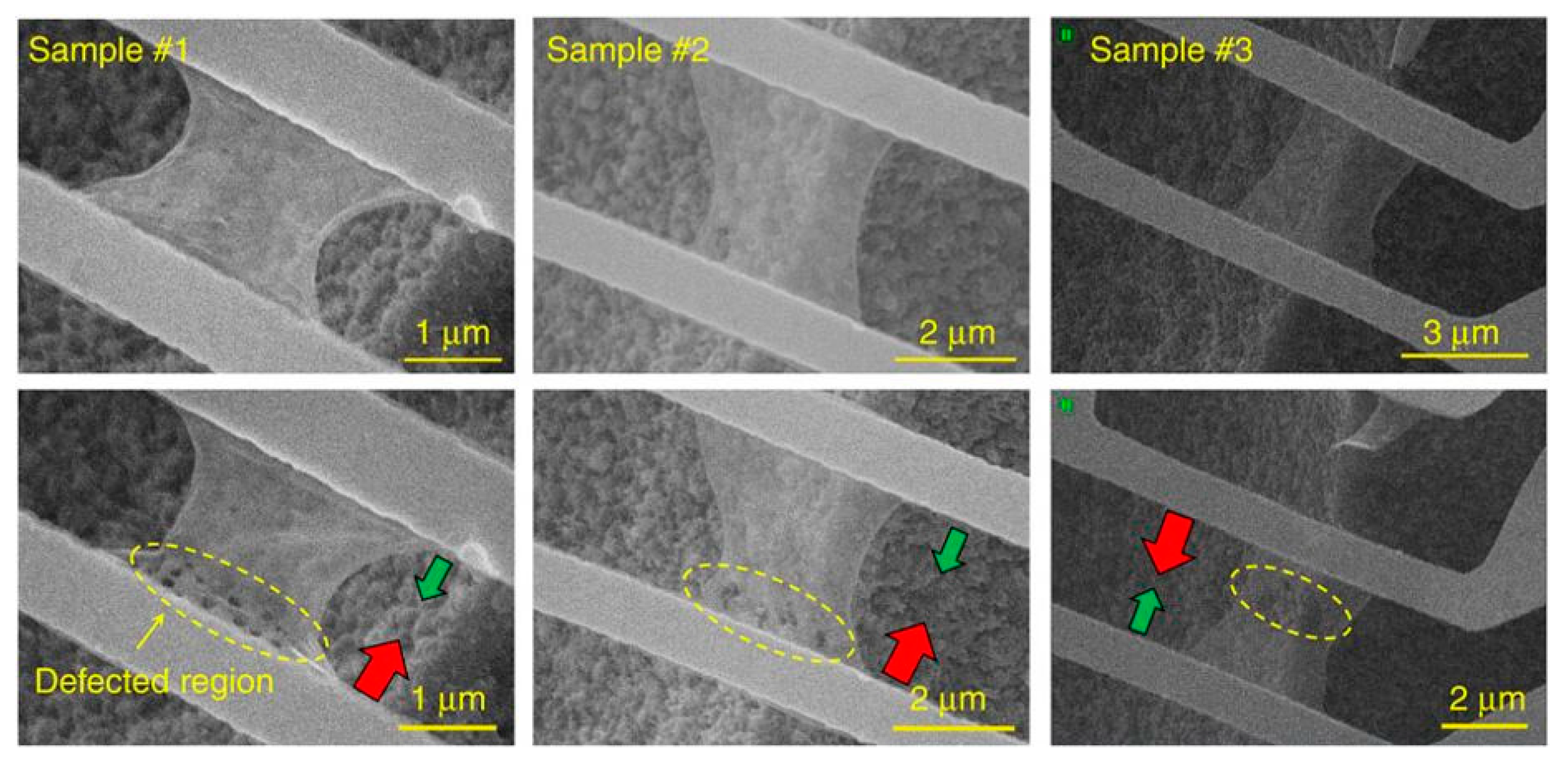
Figure 5 shows the suspended graphene with asymmetric nanopores. Large-area monolayer graphene was prepared by a method previously proposed for graphene fabrication [
37,
38]. Samples 1, 2, and 3 in
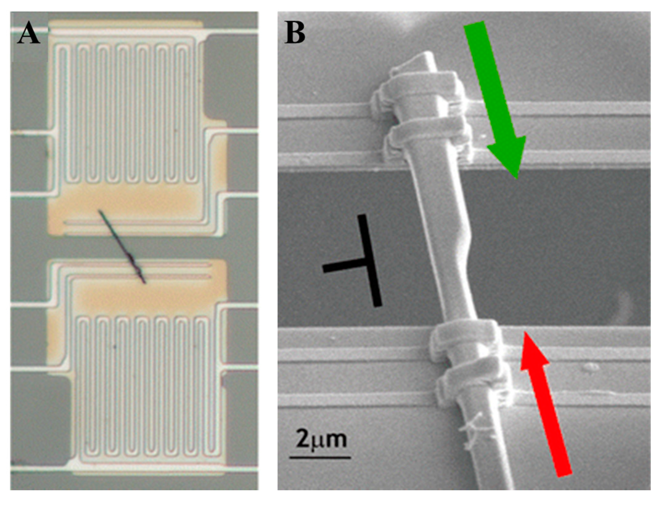
Figure 5 were asymmetry-modified using a focused ion beam (FIB) method. At one side of graphene, 14 nanopores with a diameter of 100 nm, 6 nanopores with a diameter of 200 nm, and 3 nanopores with a diameter of 400 nm were drilled. In order to measure the direction-dependent thermal conductivity precisely, a H-type sensor method was used. The advantage of the H-type sensor method is that it is easy to change the heat flow direction by simply changing the electrical heating power of two sensors. The nano-film sensor can guarantee the high precision of thermal measurement on monolayer graphene [
39].
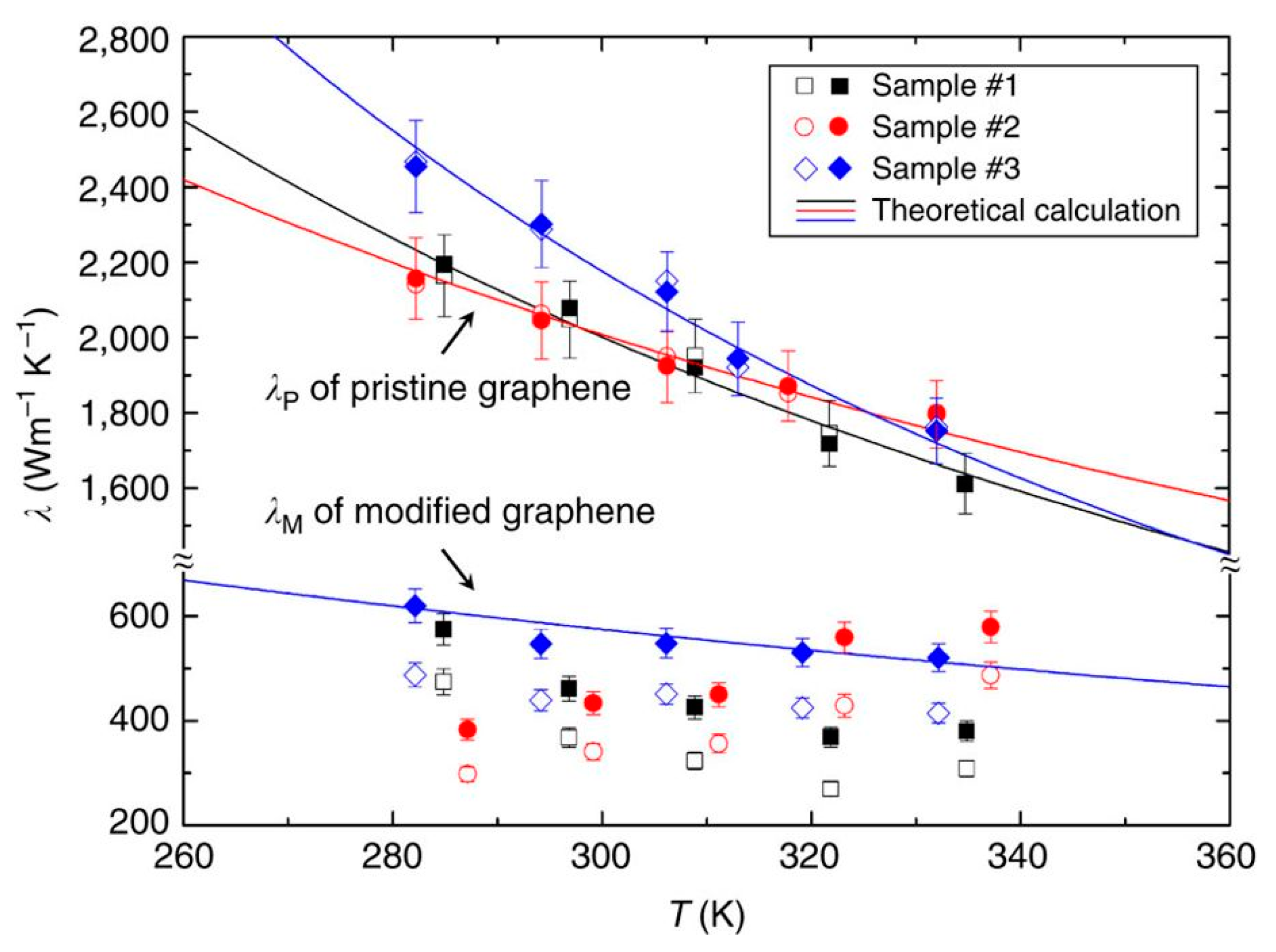
Measurements of pristine graphene without nano-processing showed no rectification effect. The difference between the thermal conductivities of the same graphene sample in two heat flow directions was less than 2%, as shown in
Figure 6. For the graphene with asymmetric nanopores, the thermal conductivity of the sample is larger in the heat flow direction from the perforated region to the unperforated region. The measured thermal rectification factor was up to 26%. The cause of this phenomenon is the asymmetric temperature/space dependence of the thermal conductivity of graphene. The thermal conductivity of pristine graphene in the unperforated region decreases as the temperature increases, while the thermal conductivity of graphene in the perforated region is almost independent of temperature due to the significantly enhanced phonon-defect scattering. It is worth mentioning that this asymmetric thermal conductivity is dominated by phonon transfer, while the electron contribution is symmetrical here [
40]. The average thermal conductivity of perforated graphene is only 10–20% of that of pristine graphene. Meanwhile, the thermal rectification coefficient was calculated by using a series of thermal resistance models, giving a value of 28%, which was consistent with the experimental results. In addition, Schmotz et al. has demonstrated a thermal diode consisting of an array of differently shaped holes milled into silicon membrane under the same mechanism [
41].
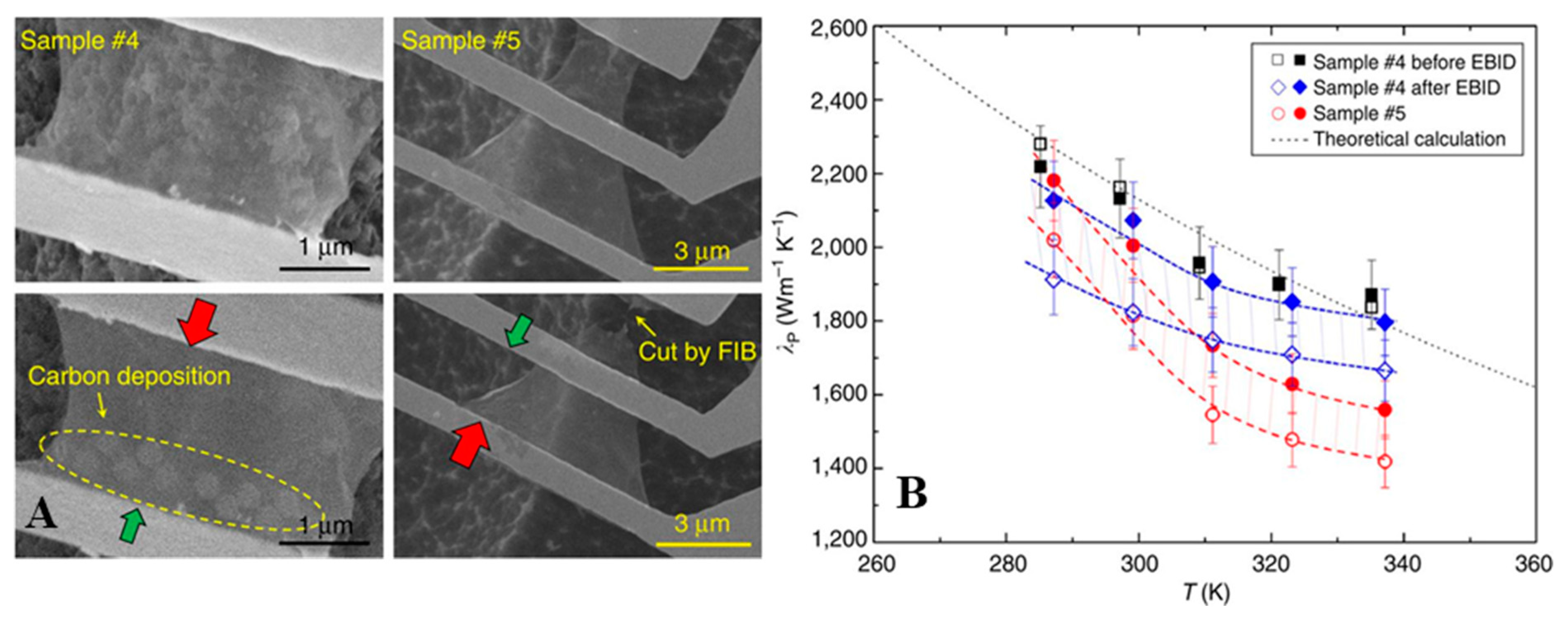
Sample 4 in
Figure 7 is the suspended graphene with 10 amorphous carbon nanoparticles deposited at one side by using the electron beam-induced deposition (EBID) method. The diameter of nanoparticles is about 200 nm. Sample 5 in
Figure 7 is the suspended graphene cut into a trapezoid shape. The asymmetric structure of the graphene sample causes a thermal rectification effect. The thermal conductivities of Samples 4 and 5 were measured by using the H-type sensor method. It was found that the thermal conductivity of Sample 4 is larger in the heat flow direction from the smooth region to the deposition region, and the measured thermal rectification coefficient is 10%. Similarly, Sample 5 has a higher thermal conductivity as heat flows from the wide region to the narrow region, and the measured thermal rectification coefficient reaches 11%. In both cases, the thermal rectification effect is caused by the asymmetric two-dimensional geometries. This results from the strong spatial and temperature dependence of the heat conduction of phonons in graphene. Due to the phonon edge scattering effect [
42], the mean free path of the narrow end of graphene is smaller than that of the wide end. At the same time, since the phonon population density on the hot side of graphene is higher than that on the cold side, if the narrow end is placed on the hot side, the edge scattering effect will impose more restrictions on the propagating phonons and cause a bottleneck effect. As a result, the thermal conductivity in the heat flow direction from the narrow end to the wide end is smaller than that in the opposite direction. The thermal rectification effect in Sample 4 follows the similar principle that the carbon atoms deposited on graphene cause stronger phonon scattering, which reduces the mean free path of phonons and plays a similar role to the narrow end of the trapezoidal graphene. Therefore, the thermal conductivity in the heat flow direction from the deposition region to the smooth region is lower than that in the opposite direction. It is worth mentioning that Wang and Ruan et al. conducted similar work independently in 2014, and realized a thermal rectification in asymmetric graphene nanoribbons with a rectification ratio up to 10% [
8].
This work experimentally verified two different physical mechanisms of the thermal rectification phenomenon in suspended monolayer graphene, providing inspiration for the future design of two-dimensional thermal rectifiers.
2.4. Thermal Rectification in Vanadium Dioxide Beams
As early as 2009, Kobayashi et al. has experimentally demonstrated an oxide thermal rectifier in bulks, consisting of two cobalt oxides with different thermal conductivities depending strongly on temperature [
43]. Here, Majumdar and Zhang et al. experimentally realized an oxide thermal rectifier in vanadium dioxide microbeam with different physical mechanism, which can be switched between two states by controlling the temperature [
44]. Up to 28% thermal rectification is observed in the rectifier state, while the thermal rectification effect disappears in the resistor state (<1%).
Previous work has shown that thermal rectification occurs in a single metal–insulator interface composed of CuO-Cu. Polycrystalline VO
2 has been shown to undergo metal–insulator transition at the transition temperature of around 340 K and there exists a mixed metal–insulator interface in the VO
2 beam below 340 K [
45]. The thermal rectification experiment was designed based on the unique metal–insulator transition property of VO
2. In this work, the VO
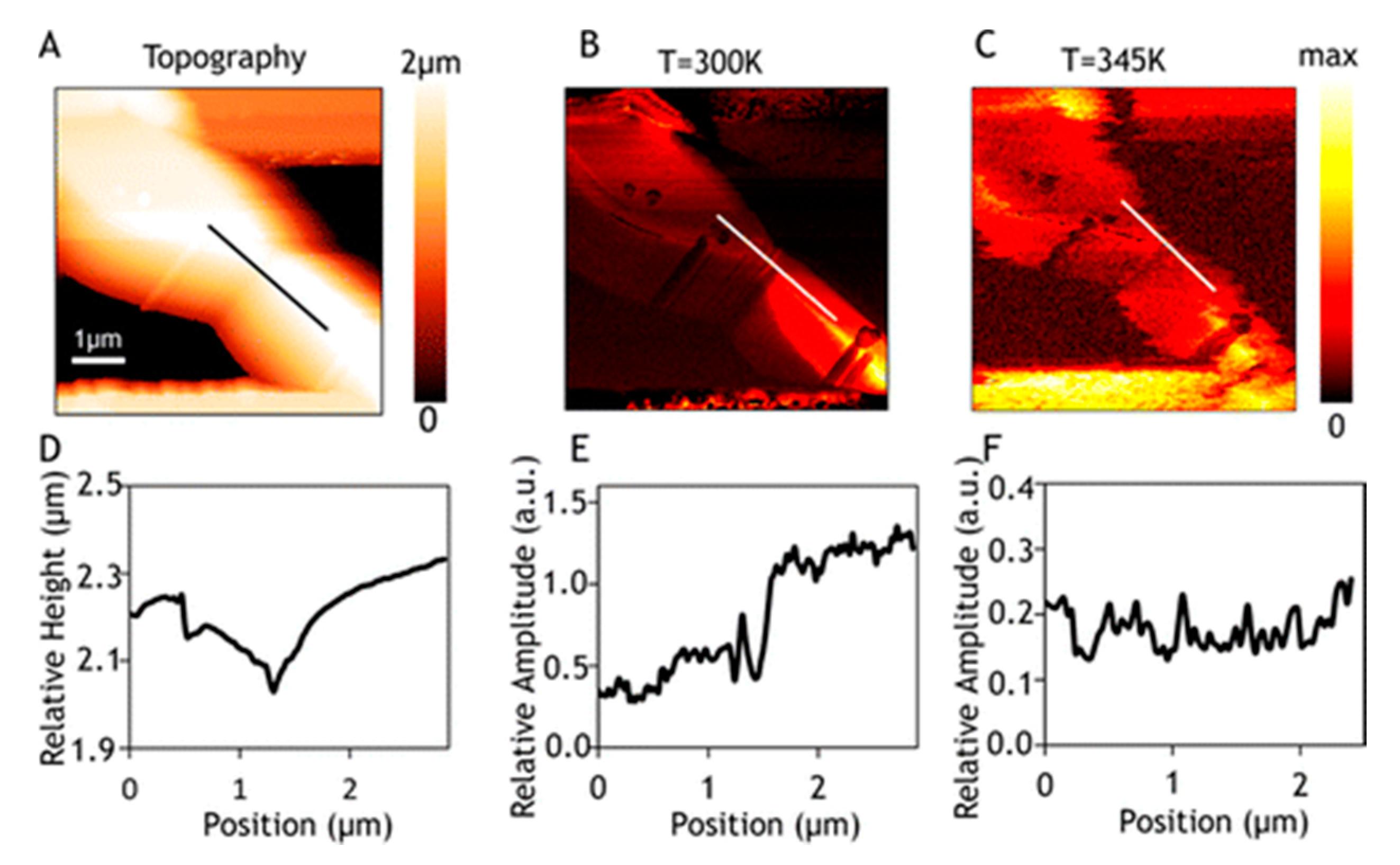
2 beams were synthesized by a modified vapor transport method and a tapered sample was selected for experiment, as shown in
Figure 8B. The biaxial thermal conductivity was measured by using a typical micro-thermal bridge method. Several SiNx beams were used to support the suspended sample and two platinum coil electrodes were used as a heater and a resistance thermometer, respectively. A focused ion beam was used to deposit platinum/carbon composite symmetrically at both ends of the sample to enhance electrical and thermal contact. The biaxial thermal conductivity measurement can be easily done by changing the electrical heating power of each platinum electrode.
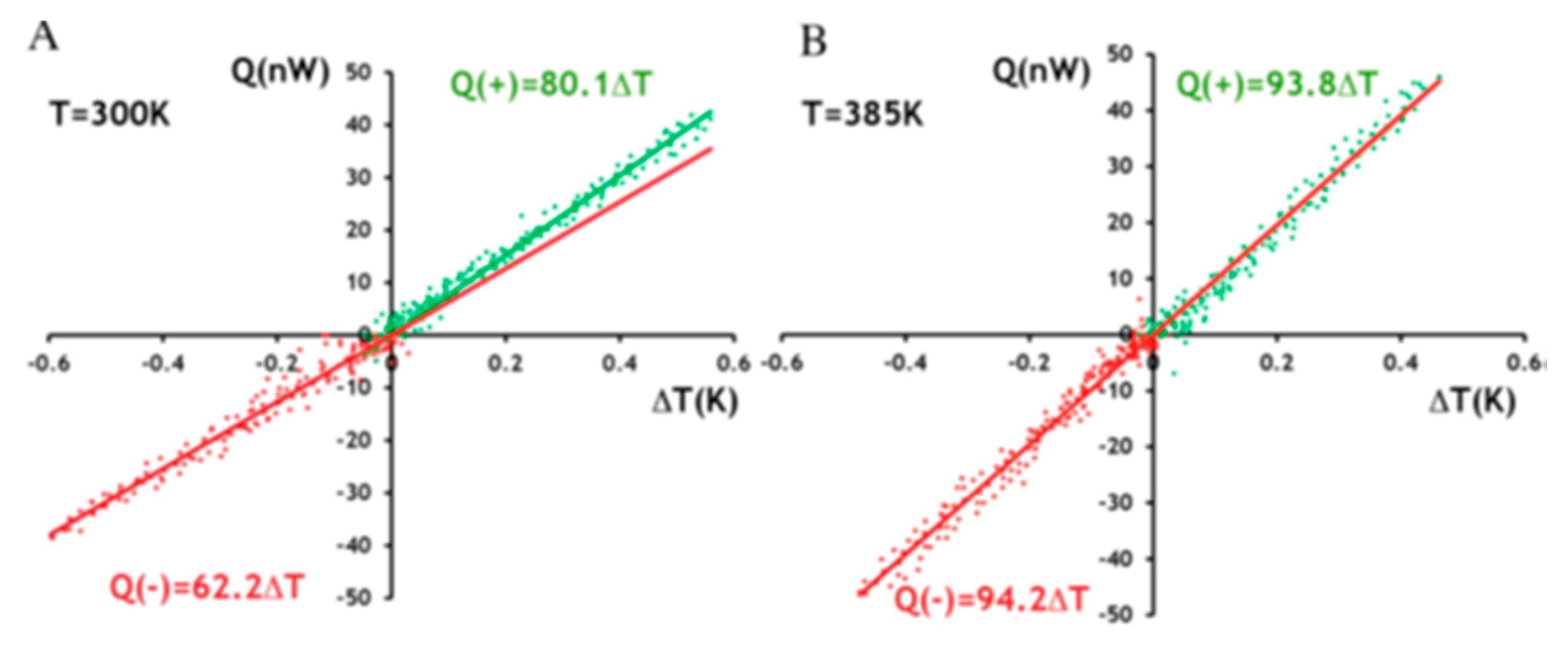
The results of temperature deference and heat flow shown in the
Figure 9 were measured at 300 K (below a transition temperature of around 340 K). As the temperature difference increases, the heat flow increases linearly. In the slope between heat flow and temperature difference, characterization of the thermal conductivity is different. The thermal conductivity when heat flows from the narrow side to the wide side is significantly smaller than that in the opposite direction, which represents 28% ± 1.4% thermal rectification. However, at 385K when the VO
2 beam is completely metallized, the experimental results show no thermal rectification and the bidirectional thermal conductivity was higher than the value at low temperatures.
The thermal conductivity is smaller when heat flows from the narrow side to the wide side, where the effect of the asymmetric geometry on the mean free path of phonons due to its tapered shape needs to be considered. However, it has been estimated that the size of the cross section of the VO
2 beam is approximately 1000 times larger than the mean free path of phonons, thus the thermal rectification effect caused by the asymmetric geometry dominated by the boundary scattering effect is unlikely. On the other hand, the thermal resistance at the metal–insulator interface is caused by both phonon-electron scattering and phonon-phonon coupling. Furthermore, Lee et al. found that electronic thermal conductivity in metallic vanadium dioxide is anomalously low, which violated the Wiedemann–Franz law [
46]. The phonon-electron scattering dominates the interface thermal resistance because the lattice distortion is less than 1% in VO
2 crystals, which causes perfect acoustic matching and greatly reduces the phonon coupling resistance. Under these circumstances, the difference between the electron–phonon cooling rate and the phonon-electron cooling rate explains the cause of thermal rectification near the interface. Moreover, the observation of thermal rectification requires a distinct asymmetry throughout the mixed phase, which can be verified by a scattering type scanning near-field optical microscope (s-SNOM). The principle of s-SNOM is that the regions of the metallic phase can cause a higher s-SNOM amplitude signal than the insulating phase due to its larger effective tip−sample polarizability. The mixed phases can be directly observed by comparing the s-SNOM signal amplitudes between the metallic and insulating phases.
Figure 10 compares the s-SNOM images at 300K and 345K. It shows that at 300K the narrow end of the tapered VO
2 beam is metallic while the wide end is insulating. When the temperature is heated to 345 K (above the transition temperature around 340 K), this notable amplitude difference between two phases disappears. Similarly, no difference in signal amplitude was noticed in a VO
2 beam with a uniform cross section. This demonstrates that the asymmetry of the internal mixed phase due to the tapered structure is the cause of the thermal rectification effect.
In this work, a thermal rectification device controlled by ambient temperature was realized. The maximum thermal rectification coefficient was observed to be 28% at 320 K, and the thermal rectification effect disappeared when the temperature exceeded the transition temperature at 340 K. This study provides a new research direction in which the interplay between the metallic and insulating phases can realize active thermal control. Moreover, VO
2 has a wide range of applications due to its unique phase change behavior. For example, Kota Ito et al. has experimentally demonstrated a radiative thermal rectifier in the far-field regime with a thin film VO
2 deposited on the silicon wafer [
47]. Wang and Wu et al. designed and implemented a novel, all-solid-state thermal switching device by nanostructured phase transformation of VO
2 thin film [
48].
2.5. Thermal Rectification of Electronic Heat Currents
Recent theoretical studies have shown that the thermal rectification effect of the electronic heat current can be achieved in tunnel junctions of metal microcircuits at low temperatures [
49,
50,
51]. Giazotto et al. confirmed the feasibility of this thermal diode through experiments [
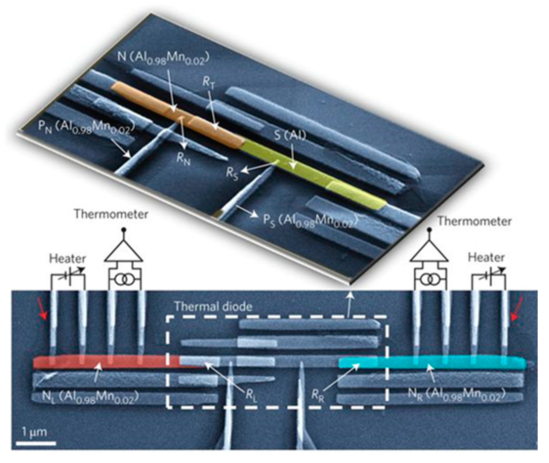
52]. They used electron beam lithography, metal mask and in situ oxidation to design a N
LINISIN
R chain, where N represents common metal (composed of Al
0.98Mn
0.02), I represent insulator, S represents superconductor (composed of Al with critical temperature at 1.5 K), and subscripts L and R refer to the left and right leads, respectively (
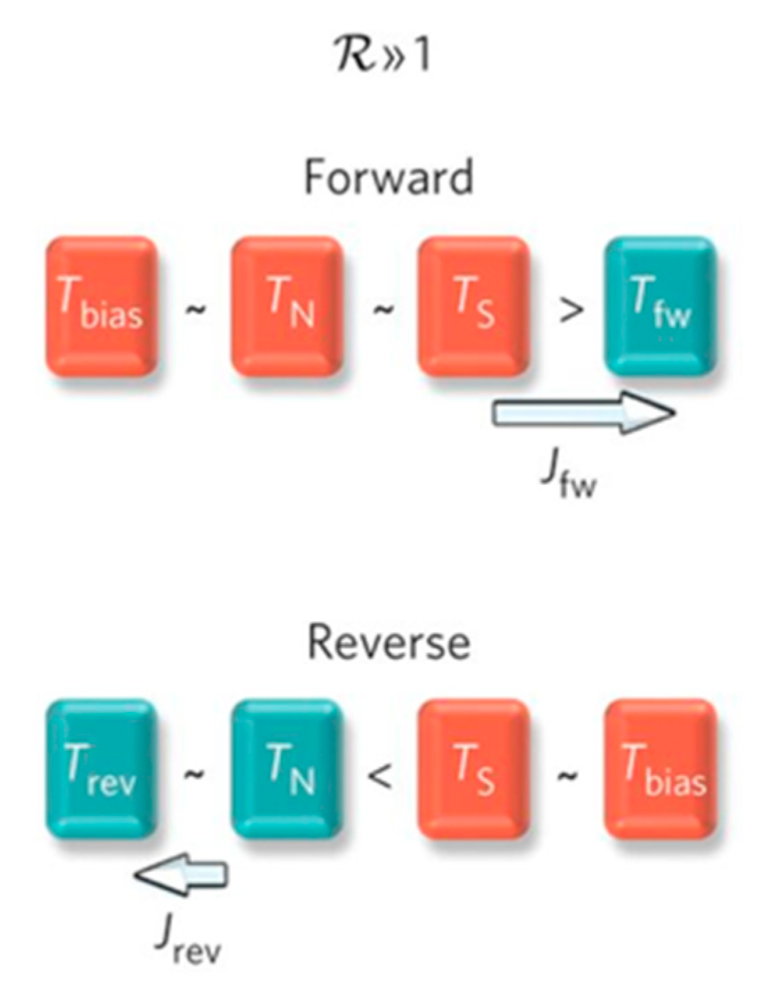
Figure 11). The thermal symmetry is destroyed by inserting the S electrode into a common metal diode such that the normal-state resistance on the right side is much larger than the resistance on the left side. Here, the presence of band gap significantly suppresses the heat flow through the S electrode. Two common metal probes and four superconducting probes were prepared on both sides of the sample, which can be used as both a heater and detector. The thermal resistance could be measured in both directions by changing the role of the heater and detector.
In the experiment, only the heat flow carried by the electrons was considered while the contribution of the phonons was ignored. This assumption is expected to hold because the lattice phonons in the entire sample structure were thermalized at the substrate temperature due to the very small Kapitza resistance at low temperatures [
53,
54,
55]. Therefore, it is possible to increase the electronic temperature at one end and yield a temperature gradient across the thermal diode. The experimental results are shown in
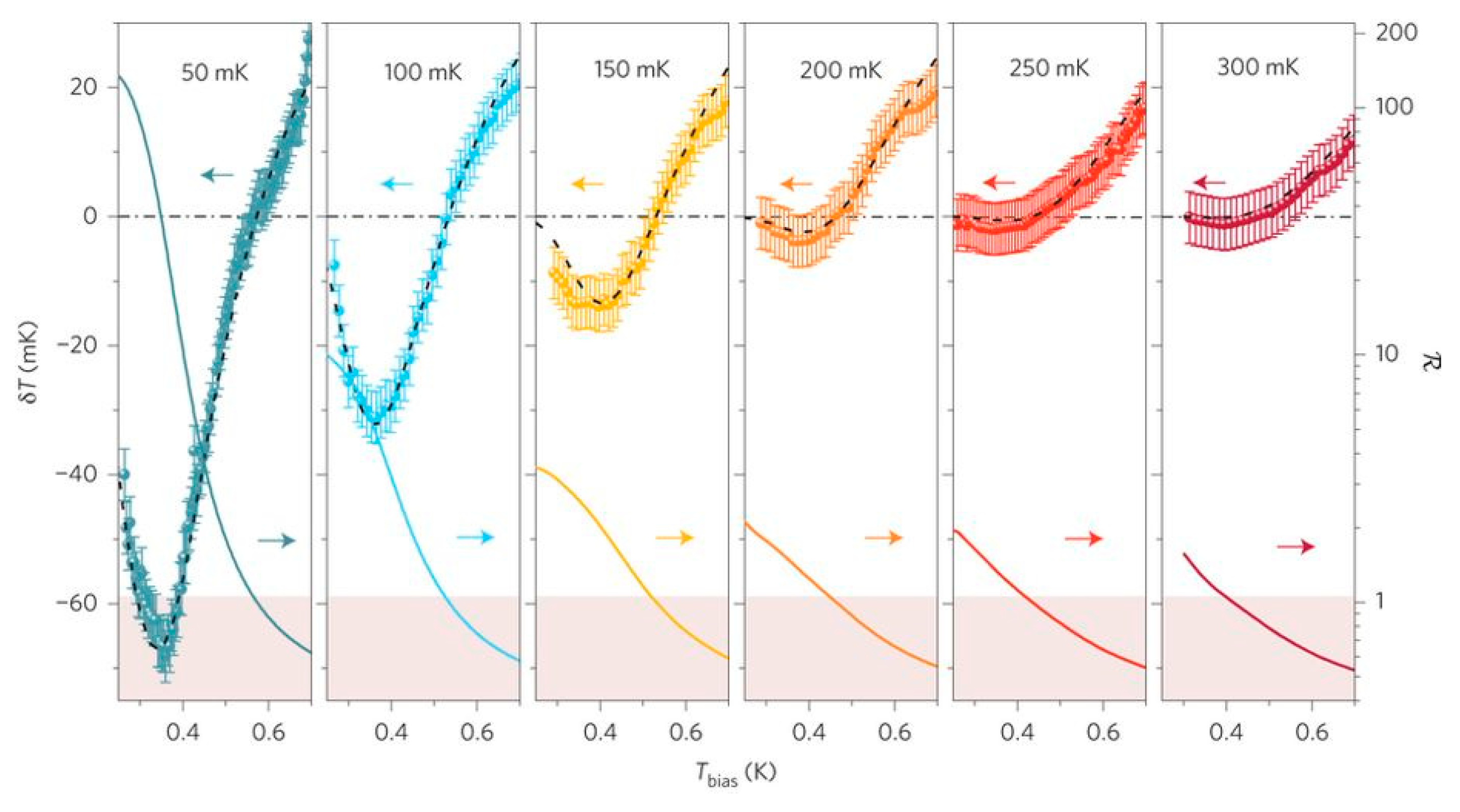
Figure 12 below. The temperature difference between positive and negative directions is drawn at different bias temperatures. The theoretical solution calculated by the thermal model is also included in the figure. It is seen that the experimental and theoretical results agree very well with each other. The thermal rectification ratio
R is marked on the right axis. It can be seen that at low ambient temperatures,
R is much larger than 1, confirming a very strong thermal rectification effect in the thermal diodes.
The presence of the superconducting electrode S is important for thermal rectification. Because the quasiparticles with energy less than the band gap cannot pass through the forbidden band, there is a large temperature difference at both ends of S. This results in the increasing temperature difference across the S-electrode in the forward temperature bias, while in the reverse, the S-electrode suppresses the temperature difference and eventually causes a much larger forward heat flow and strong thermal rectification effect.
In
Figure 12, as the temperature bias increases, 1/
R > 2 occurs, which implies another thermal rectification mechanism in the thermal diode. The energy transmitted from the N-electrode to the environment has been divided into two parts: one part transmitted to the bath temperature by the cold finger probe is correlated with the quadratic square of the temperature (
), and the other part is transmitted by the lattice phonons, which is related to the sixth power of the temperature
. As
Figure 13 shows, when the temperature bias in the system increases, the second part of the energy exceeds the first part, which becomes a dominant contribution in the heat conduction. This leads to an enhanced electron–phonon coupling and effectively suppresses the forward heat flow. The increase in ambient temperature will accelerate the latter’s share of the former and further decrease the forward heat flow. The energy gap of the superconducting electrode is also affected by the bath temperature, causing an increase in the reverse current. For all the above reasons, the bath temperature was 300 mk, the temperature difference was 700 mk, and 1/
R reached 2.
This experiment designed a thermal diode with a significant thermal rectification effect, providing ideas for the design of cryogenic solid-state thermal circuits.
3. Discussion
In this brief review, we have summarized some recent experimental approaches for realizing thermal rectification at the nanoscale and their underlying physical mechanisms. At the bimaterial nanocontact interface, the localized phonon modes are generally gathered at the edges and suppress the heat flow from the polyamide nanofiber to silicon nanowire. In the asymmetric nanotubes, the thermal conductivity was found to be larger in the heat flow direction from the high mass-loaded end to the low mass-loaded end. Such thermal rectification in the asymmetric one-dimensional system cannot be fully explained by the conventional phonon-edge scattering model while the soliton theory provides a reasonable explanation. In the suspended graphene, thermal rectification was realized by creating nanopores, loading nanoparticles at one side or cutting the membrane into a tapered shape. The asymmetric temperature dependence of thermal conductivity and significant lateral confinement of two-dimensional phonons are found to be the reason. In a tapered VO2 beam, thermal rectification was observed below the metal–insulator transition temperature. In this system, the asymmetric electron–phonon coupling at the metal–insulator interface is the possible reason for rectification. At cryogenic temperature, significant thermal rectification in the electronic heat current was realized at normal metal-superconductor tunnel junctions. The selective electronic heat flow across the superconducting electrode and enhanced electron–phonon coupling at the normal metal electrode are found to be the reason for thermal rectification. All of these pioneering experiments demonstrate the feasibility of designing efficient thermal diodes at the nanoscale through advanced nanofabrication techniques. A large thermal rectification ratio can be achieved by creating an asymmetric nanocontact interface, mass-loaded nanotube, defect-engineered two-dimensional material, metal–insulator contacting phase or cryogenic superconducting tunnel junctions. Unique and rich physics have been revealed in these nano-thermal rectifiers, but much more remains to be explored. There is no doubt that our rapid growing ability of precise nanofabrication will greatly enlarge the research of logical thermal circuits and become one of the key technologies in thermal sciences.


