Article

Free Space Optic Receiver with Strongly Overlapped Photodetectors’ Field of View

Department of Telecommunications, Faculty of Electrical Engineering and Computer Science, VSB–Technical University of Ostrava, 708 33 Ostrava, Czech Republic
*
Author to whom correspondence should be addressed.
Appl. Sci. 2019, 9(2), 343; https://doi.org/10.3390/app9020343
Submission received: 9 December 2018 / Revised: 10 January 2019 / Accepted: 17 January 2019 / Published: 19 January 2019
(This article belongs to the Special Issue Light Communication: Latest Advances and Prospects)

Abstract

:
In this study, we designed a mobile free space optic receiver that uses several photodetectors to provide omnidirectional receiving capability. Assuming only one transmitter, it is a receiver which builds a single input multiple output optical channel. The photodetectors are fixed to truncated pyramid walls. Electrical signals from the photodetectors are processed using an equal gain combining technique. This architecture allows simple circuits and enables additive noise suppression. The minimum angle between the pyramid base and the direction of falling rays was calculated to determine the threshold for additive noise suppression. Two areas of interest presented themselves: the processing of very weak electrical signals often drowned in noise, and optimization of the number of photodetectors whose fields of view overlapped strongly. We outline the design of the optical receiver circuitry and provide some practical hints concerning its assembly. The receiver was evaluated using bit error rate measurements and comparing signal-to-noise ratio parameters for various photodetector numbers. The measured data confirm the theoretical assumptions.

1. Introduction

The goal of this study was to design a mobile free space optic (FSO) multiple photodetector receiver optimized for highest sensitivity and communication radius. The mobile FSO receiver has no fixed position or fixed distance between the optical transmitter and the receiver. There is also no fixed angle between the main lobes of a transmitter’s and receiver’s components. All these factors complicate noise optimization [1]. An ideal mobile optical receiver responds to signals coming from an entire sphere. Assuming that the transmitter is above the receiver, the spatial angle might be reduced to half, i.e., one hemisphere, 2π sr. The receiver will be still sensitive to noise from the whole hemisphere, whereas the useful signal might only come from a part of it. An outdoor environment without reflections serves as a typical example. Interiors, however, offer much better receiving conditions due to numerous reflections, and all directions detection capability is beneficial. Similarly, scattering of ultraviolet light improves the receiving conditions, even in open space [2,3,4]. Therefore, the receiver should be designed with regard to the planned environmental conditions and spectral characteristics of the light to be used.

1.1. State-of-the-Art

Many approaches have shown how to manage omnidirectional receiving capability. Based on optical to electrical conversion, these approaches can be classified into three fundamental groups.
The first group of receivers employs only one photodetector and some additional optical elements, for example, the fish eye optical system mainly used in robotics [5,6]. A system using two mirrors, similar to telescope systems, serves as another example [7,8]. An omnidirectional stereo imaging system uses a concave lens and a convex mirror [9]. Other assemblies use non-imaging collectors, such as compound parabolic concentrators (CPCs) in an array-like fashion [10,11] or a fiber bundle that couples omnidirectional photons in its field of view (FOV) and delivers these photons to the detector [12,13].
The second group of receivers employs several photodetectors with a signal-combining technique. The first example of these is called selection combining (SC), which uses only one detector with the strongest instantaneous signal from s-detectors for signal detection [14]. The second technique is called maximum ratio combining (MRC), where all s-detectors are selected and coherently combined with the gain of each channel proportional to the root-mean-square (RMS) signal level and inversely proportional to the mean square noise level in that channel [15]. In other words, this technique follows the rule of optimal filtering. The third technique is known as switched combining. Detectors are switched once the signal collected by the active detector falls below a predetermined threshold. Because of this, switching does not occur as often compared to SC [16]. The last technique is equal gain combining. The signals from all s-detectors are summed coherently and with an equal gain [17].
The third group consists of receivers with hemisphere-photomultiplier tubes. Typical examples were presented in Puschell, J. et al. [2], Farr, N. et al. [18], Liu, X. et al. [19].
Note, the overview given above is not comprehensive.

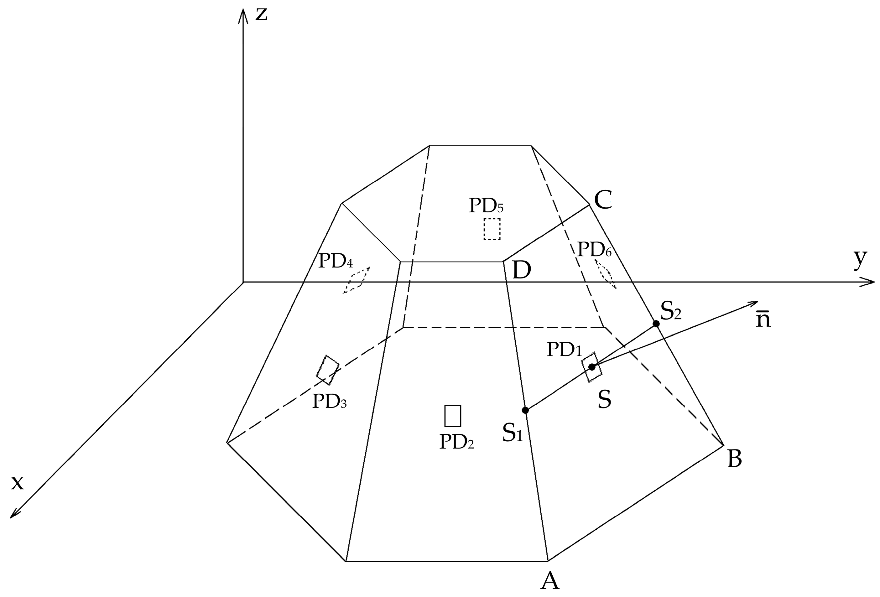
1.2. Receiver Concept

The receiver described below belongs to the second group of receivers and uses the equal gain combining technique. In this receiver, all photodetector signal currents are summed and processed as a whole instead of switching to the strongest signal photodetector.
The aim of this study was to highlight the merits of the equal gain combining technique and describe the same technique in receiver design. Many papers have already discussed multiple photodetector combining techniques, but all of them mainly focused on a mathematical description of optical channels. We focused solely on receiver design. The described receiver also differs in the degree of FOVs overlap. Whereas most papers describe multiple photodetector receivers with only slight or no FOVs overlap, the present receiver works with a large FOVs overlap. In this case, highly overlapping FOVs are valuable for additive inherent noise suppression. The set of photodetectors thus formed forms a parallel amplifier. More information can be found in previously published reports [20,21,22,23,24,25].
For the physical realization of the receiver, the omnidirectional receiver was designed using six photodetectors, PD1 to PD6, which are attached to the walls of the truncated pyramid (Figure 1). The pyramid ground plan is hexagon and its walls and base are at a 45° angle. The photodetectors are mounted on small printed circuit boards (PCBs) and are connected with the following amplifiers, which are located on a separate board below the base of the pyramid. The connections between photodetectors and the following amplifiers had to be as short as possible. For this reason, the photodetectors were finally moved from the centers of the segments to their edges.

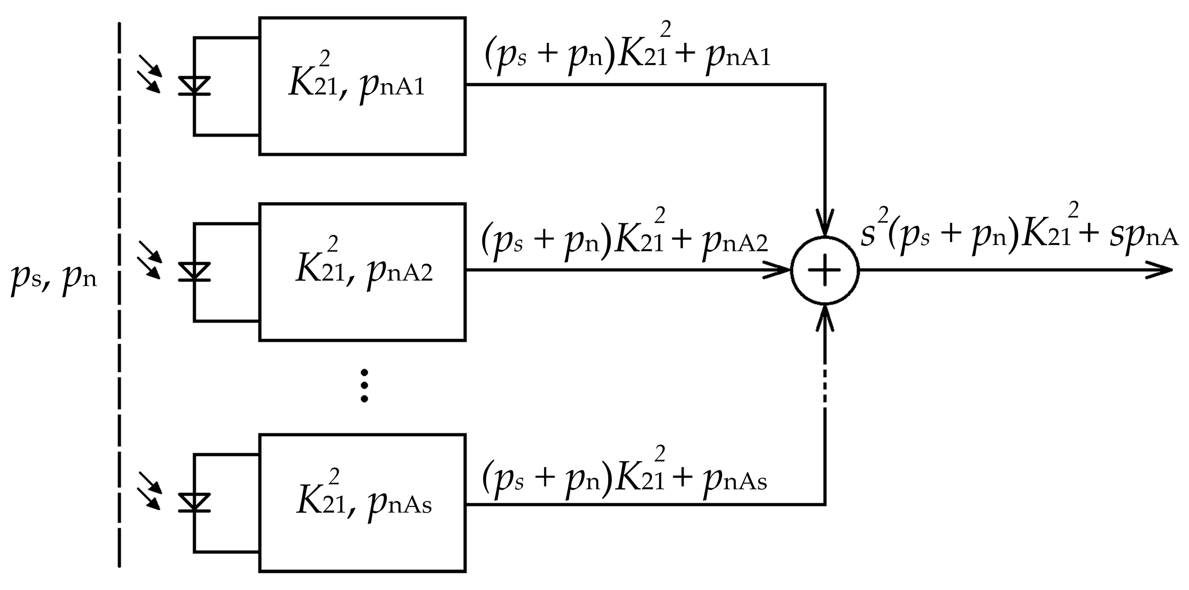
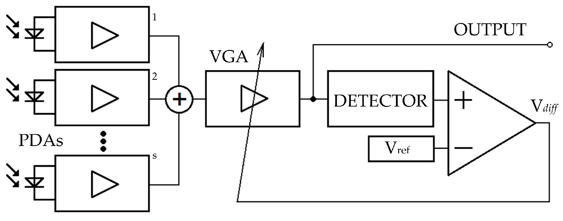
1.3. Parallel Amplifier Topology

Before proceeding to the problem of parallel amplifying and receiving with several photodetectors, the receiving using only one photodetector was analyzed.
It is important to separate the optical and electrical parts of signal detection [26] and to determine in which part noise might prevail. Written mathematically, the signal-to-noise ratio SNRin in the photodetector’s optical part is given by the total captured useful signal power ps to the total captured noise power pn in an optical channel:
S N R i n = p s p n   [ / ] .
The electrical part of the optical photodetector has a larger number of factors. Noise from the photodetector itself and the follow-up amplifier must be considered. Let this noise be expressed by the quantity pnA. The signal-to-noise ratio (SNR) in the photodetector’s electrical part is given by:
S N R o u t = p s K 21 2 p n K 21 2 + p n A   [ / ] .
The ps/pn ratio is given by the photodetector’s optical part and there is no possibility of increasing the ratio in the photodetector’s electrical part. However, if sufficient power amplification K212 is not available, the final signal to noise ratio SNRout is much lower due to pnA.
The SC technique can produce the highest SNRin since the spatial angle, along with unwanted spurious signals, is reduced. However, complexity and low reliability come as trade-offs. Note, no easy way of recognizing the strongest signal photodetector exists. Many interference optical signals are due to, for example, artificial illumination, sunlight or lightning, which might be stronger than the optical signal used and can confuse even the strongest signal photodetector selection circuit.
The parallel amplifier accommodates s photodetectors and their follow-up amplifiers, which work continuously in a common resistive load (Figure 2). Let all photodetectors have uniform signal and noise coverage. The useful optical signal power ps, together with optical noise power pn, enter the receiver in the same way. The total useful signal and noise currents must be s times higher than those for one photodetector, and similarly, the total useful signal and noise powers must be s2 higher than those for one photodetector. Each photodetector and its follow-up amplifier contribute their own noise power pnA. Since all photodetectors are standalone components, their noise powers are uncorrelated and expressed as pnA1, pnA2, …, pnAs. To prove the merits of a parallel amplifier, its uncorrelated noise powers must be summed. The procedure is as follows [27]:
Let the random and uncorrelated sequences Xn, n = 1,2,…,N and Ym, m = 1,2,…,N have the same number of realizations N such that each member of the first sequence Xn makes N possible sums with the members of the second sequence Ym. This is mathematically expressed as Xn + Ym, where m = 1,2,…,N. Since the sequences are the same size, N2 sums with different indexes nm exist as a result.
The mean power value of the sum of the single Xn sequence member and the all Ym sequence members can be written as:
1 N m = 1 N ( X n + Y m ) 2 = 1 N m = 1 N X n 2 + Y m 2 + 2 X n Y m = X n 2 + 1 N m = 1 N Y m 2 + 2 X n 1 N m = 1 N Y m .
If the Ym sequence mean value is zero, then the last part of Equation (3) must also be zero. Equation (3) can be shortened to:
1 N m = 1 N ( X n + Y m ) 2 = X n 2 + 1 N m = 1 N Y m 2 = X n 2 + Y 2 ¯ .
The mean power value of the sum of the two whole sequences can be found in the same manner:
( X + Y ) 2 ¯ = 1 N n = 1 N ( X n 2 + Y 2 ¯ ) = X 2 ¯ + Y 2 ¯ .
Equation (5) may be generalized for an arbitrary count of the unA1, unA2, …, unAs sequences, which are voltage realizations of noise powers pnA1, pnA2, …, pnAs. For pnA1 = pnA2 = … = pnAs conformity, Equation (5) can be rewritten as:
( u n A 1 + u n A 2 + + u n A s ) 2 ¯ = s u n A 2 ¯ = s p n A .
After this, the SNR in the photodetector’s electrical part, in Equation (2), takes the form:
S N R o u t = s 2 p s K 21 2 s 2 p n K 21 2 + s p n A     [ / ] .
Due to the s2 component, pnA may be eliminated more easily. As result, SNRout will be almost equal to SNRin in Equation (1), which is desirable.

1.4. Conditions Preserving Parallel Amplifier Advantages

Generally, an FSO multiple photodetector receiver is useful mainly in multipath light propagation environments, making all photodetectors useful in signal receiving. Situations may arise where the useful optical signal reaches a lower photodetector count than the FSO receiver. This reduces the total useful signal photocurrent, though the total photodiode noise current stays the same. As a result, the signal to noise ratio SNRout in Equation (7) also becomes smaller because the shadowed photodetectors are only delivering noise. Therefore, the aim was to find some marginal conditions that ensure that the SNRout of all photodetector assemblies (PDAs) are equal to the SNRout of only one PDA in use. These conditions might be expressed, for example, by a minimum angle between the pyramid base and the direction of falling rays. Unfortunately, there is no universal minimum angle, although many minimum angles are available that vary according to the pyramid’s shape and the number of walls. The minimum angle may also be calculated for any particular case. Analytic geometry offers many powerful tools, some of which are further described. For more details, see Sedlacek, M. et al. [28], Dostal, Z. [29].
The first step is calculation of all six photodetectors coordinates. The procedure listed below is related to the calculation of the coordinates of only one photodetector. Therefore, for all six photodetectors, the calculation must be performed six times because each photodetector has a different place on the truncated pyramid. Inputs are rotx and rotz angles, eventually posy and posz distances.
Let ABCD be a square positioned initially. Its points are expressed by the vectors A = [a1 a2 a3]T, B = [b1 b2 b3]T, C = [c1 c2 c3]T, and D = [d1 d2 d3]T. These might represent the photodiode active area corners. To rotate the square on the x-axis or z-axis, the vectors must be multiplied by the matrix Arotx or Arotz, respectively, as follows:
A r o t x = [ 1 0 0 0 cos ( r o t x ) sin ( r o t x ) 0 sin ( r o t x ) cos ( r o t x ) ] ,   A r o t z = [ cos ( r o t z ) sin ( r o t z ) 0 sin ( r o t z ) cos ( r o t z ) 0 0 0 1 ] .
The operations are depicted in Figure 3a,d. Written mathematically:
A = A r o t · A ,   B = A r o t · B ,   C = A r o t · C ,   D = A r o t · D .
The shift along the y-axis or z-axis enables the matrix posy or posz as follows, respectively:
p o s y = [ 0 v y 0 ] T ,     p o s z = [ 0 0 v z ] T .
The operations are depicted in Figure 3b,c. Written mathematically:
A = A + p o s ,   B = B + p o s ,   C = C + p o s ,   D = D + p o s .
The operations above lead to the A’, B’, C’, D’ point coordinates introducing the square’s final position. For simplicity, they are renamed as points A, B, C, and D, respectively.
Knowing the final coordinates of square ABCD, the midpoint S of the square may be calculated. Now, it is rotated to calculate the vector S Z ¯ , where S and the Z are the square’s midpoint and illumination point, respectively:
S Z ¯ = Z S = ( z 1 a 1 + b 1 + c 1 + d 1 4 , z 2 a 2 + b 2 + c 2 + d 2 4 , z 3 a 3 + b 3 + c 3 + d 3 4 ) .
The screening P of the square ABCD to the plane perpendicular to the direction of falling rays, i.e., vector S Z ¯ , can be found as individual points A, B, C, D screening:
P ( A ) = A ( A T S Z ¯ ) S Z ¯ P ( B ) = B ( B T S Z ¯ ) S Z ¯ P ( C ) = C ( C T S Z ¯ ) S Z ¯ P ( D ) = D ( D T S Z ¯ ) S Z ¯ .
The final task is calculating surface Sp from the P (A), P (B), P (C), and P (D) corners:
S p = 1 2 e ¯ · f ¯ · sin ϑ .
The diagonals e ¯ and f ¯ and the ϑ angle are defined as:
e ¯ = P ( D ) P ( B ) ,       f ¯ = P ( C )   P ( A ) ,       cos ϑ = e ¯ · f ¯ e ¯ · f ¯
The procedure above may be simplified for truncated pyramid holder dimensions much smaller than the distance between this holder and the point of illumination. First, there is no obstacle to having the points A, B, C, and D stand symmetrically around the initial position [0 0 0]. Second, the operations rotx and rotz are sufficient to properly position the square; therefore, the operations posy and posz are omitted. As such, the ABCD square midpoint S holds the initial position over all rotations, and the vector S Z ¯ is reduced to the point Z coordinates.
The second step is to find all six photodetector surface screenings and their change over the φz angle (Figure 4). The illumination point Z Cartesian coordinates are calculated separately corresponding to the run along the circle, as shown in Figure 4, and they are not listed here. The only variable listed is the φz angle, which is the illumination point Z Polar coordinate (we assumed that midpoint S holds the initial position).
Let there be a truncated pyramid holder positioned according to Figure 4a, where the pyramid edge points toward the illumination source. The illumination source runs along the circle from the x-axis toward the z-axis. The change in the photodetector surface screening for segments SA, SB, and SC is depicted in Figure 4a. Similarly, let the truncated pyramid holder be positioned according to Figure 4b, where the pyramid wall points toward the illumination source. Again, the illumination source runs along the circle. The change in the photodetector surface screening for segments SA, SB, SC, and SD is depicted in Figure 4b. The total surface screening from all segments can be found by their sum independent of orientation. For case (a), the total surface screening is the sum of the SA, SB, and SC segments multiplied by 2. For case (b), the total surface screening is the priority sum of the SB and SC segments multiplied by 2 and the additional sum of the SA and SD segments. The surface screening of the shadowed photodetectors is zero. The total surface screening vs. angle φz is shown in Figure 5. All calculations were performed in Excel software (Microsoft, Redmond, WA, USA, 2007).
The minimum angle between the pyramid base and the direction of falling rays can be found as follows. Let each photodetector be described by the unit useful signal current and the unit noise current. It follows that SNRout = 1. The parallel amplifier sums the useful signal currents and the noise currents of all photodetectors. The total useful signal current will be a six-multiple of one photodetector’s useful signal current. The total noise current will be a 6 -multiple of one photodetector’s noise current. Assuming that all the sensitive areas of the photodetector are perpendicular to the direction of falling rays, SNRout will be enhanced ( 6 / 6 ) 2 times, which is six times. Since the useful signal current and the sensitive area are proportional [1], the currents and surfaces may be swapped, which matches the curve analysis shown in Figure 5.
The most advantageous situation occurs when the direction of falling rays is perpendicular to the truncated pyramid base. Each photodetector surface screening is then maximized. Assuming that the default sensitive area is equal to the unit, and the photodetectors and the pyramid base are at a 45° angle, then one photodetector’s surface screening is 1 / 2 and the six photodetectors’ surface screening is 6 / 2 = 3 2 = 4.243 . This is the same value shown in Figure 5 for the angle φz = 90°. If φz decreases, the total surface screening also decreases and reaches its minimum at φz = 0°, being slightly over 1. However, the noise level surface equivalent stays the same, being equal to 6 = 2.449 . To preserve the parallel amplifier’s advantage, the total surface screening must be higher than 2.449. This is fulfilled for angles greater than the minimum angle φz = 32°. In other words, at angle φz = 32°, the SNRout value of all PDAs is equal to the SNRout of only one PDA in use. The best SNRout is achieved for the angle φz = 90°, though the maximum value is only ( 3 2 / 6 ) 2 = 3 (or 4.8 dB). The curve breaks in Figure 5 correspond to the angles when the photodetectors in shadow become illuminated.
The calculations above have solved one particular case for a receiver equipped with six photodetectors fixed to truncated pyramid walls where the truncated pyramid walls and base are at a 45° angle. However, this is only one case out of many others. The question then arises as to design of a FSO receiver’s optimal holder for a particular application? For example, how many photodetectors is best for that application? Which pyramid wall and base angle is optimal for that application? No universal answers can be provided; therefore, our attention returns to Equation (7). The number of photodetectors collecting the useful optical signal s’ from the total number of photodetectors s can be easily separated. Equation (7) can be rearranged as follows:
S N R o u t = s 2 p s K 21 2 s 2 p n K 21 2 + s p n A     [ / ] .
Environments possessing a uniform signal coverage, such as interiors, provide reflection of light signals and lead to the equality s’ = s. Based on these conditions, an increasing s eliminates noise power pnA (the PDA noise power) and enhances the signal to noise ratio SNRout.
Environments without reflections might keep some photodetectors permanently in shadow. Since they remain without a useful signal power, the equality s’ = s is replaced by the inequality s’ < s, and the noise power pn from an optical channel determines the situation. If it is much lower than the PDA noise power, pn << pnA, Equation (16) becomes:
S N R o u t = s 2 p s K 21 2 s p n A     [ / ] .
Even here, enhancement of the SNRout may be expected because the numerator grows by the power of two of the illuminated photodetector’s number s’. Enlargement of the photodetector is again beneficial. The only problem is the non-zero noise power pn from the optical channel. With the relationship pn > pnA, Equation (16) becomes:
S N R o u t = s 2 p s K 21 2 s 2 p n K 21 2 = ( s s ) 2 p s p n     [ / ] .
Based on these conditions, even a small difference between the illuminated photodetector number s’ and the total photodetector number s will have a strongly adverse impact on SNRout. Similarly, any photodetector enlargement will deteriorate the situation.
We conclude that the FSO equal gain combining multiple photodetector receivers are suitable either for optically reflective environments or environments with a low optical noise power pn.

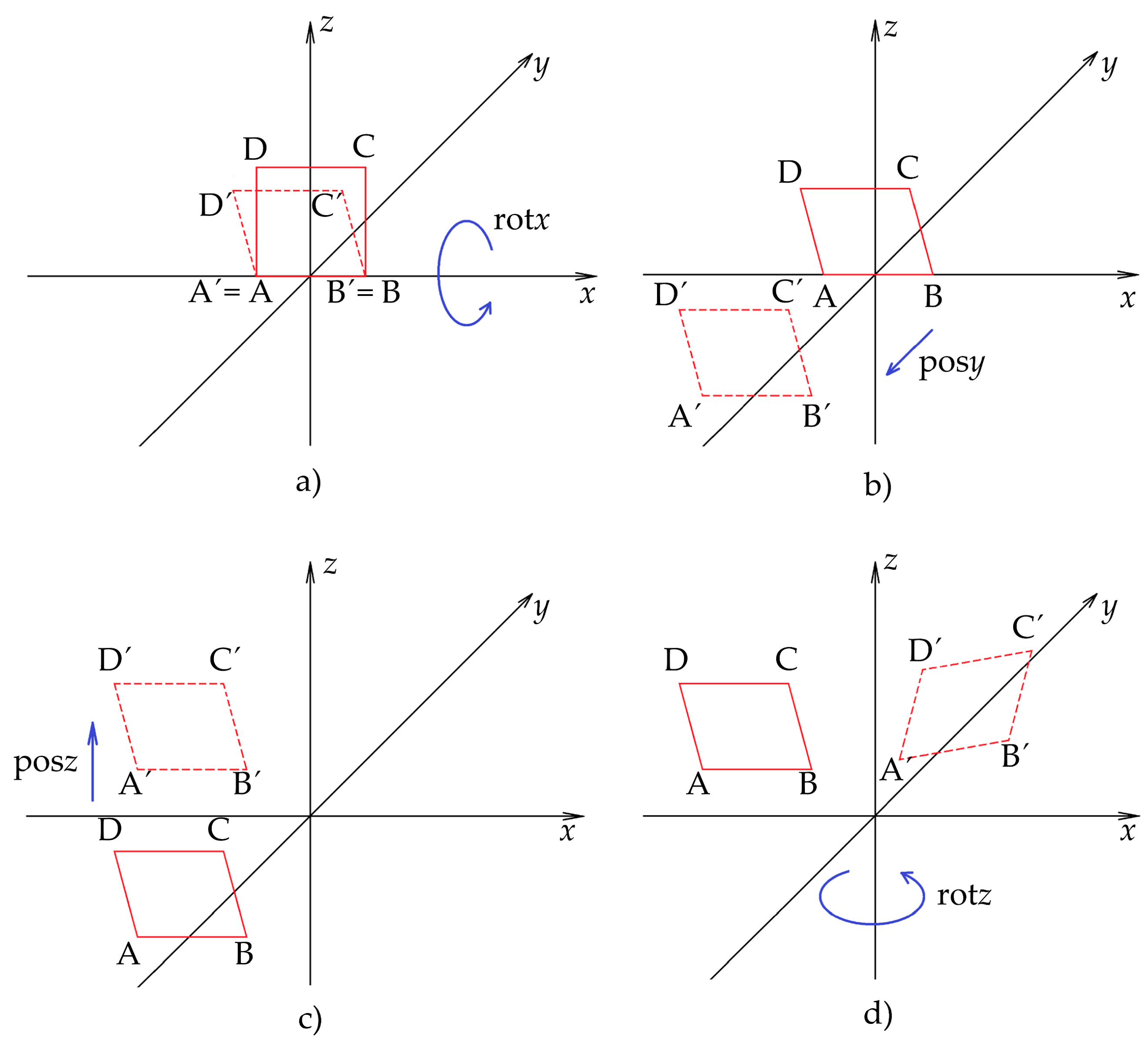
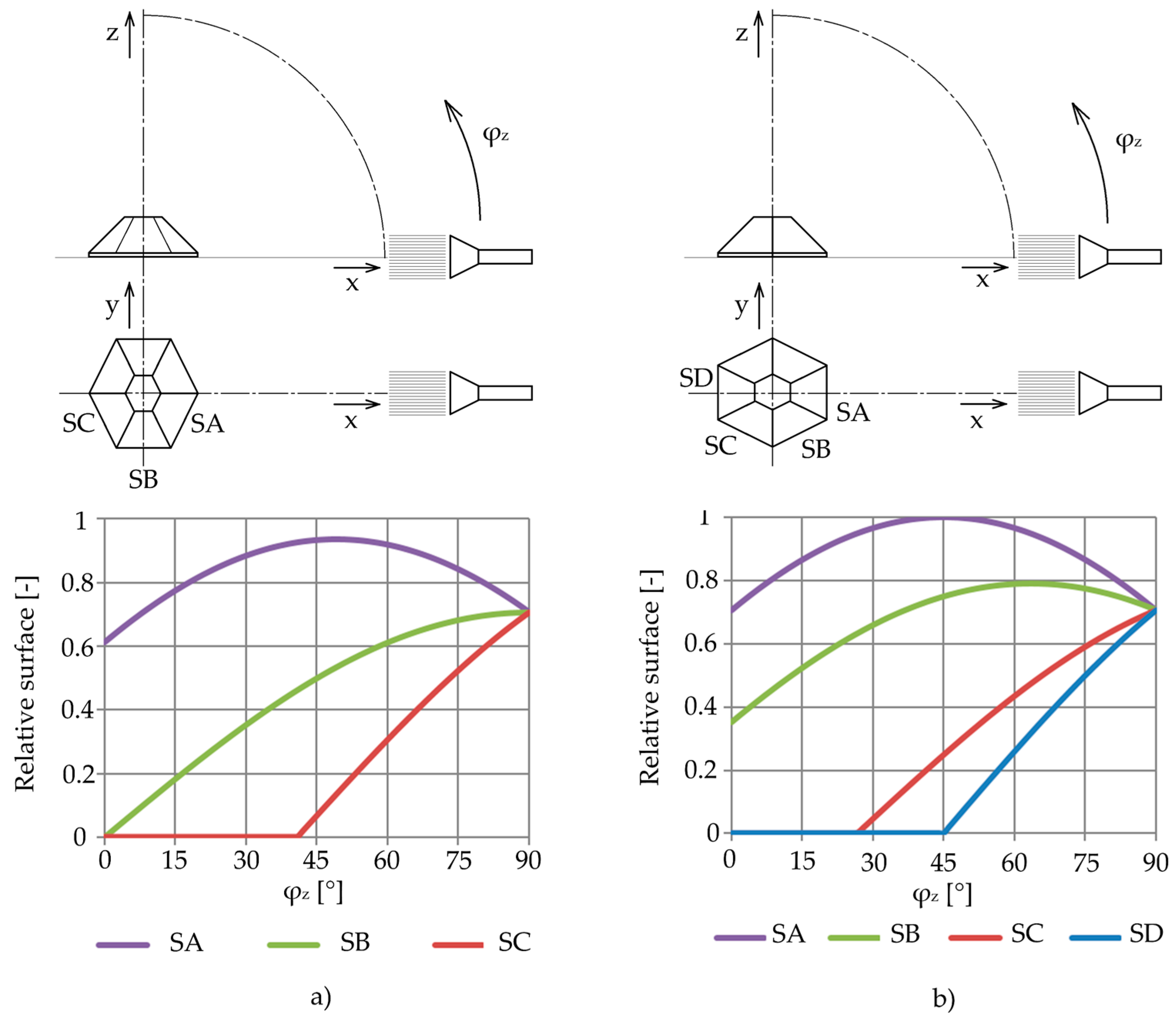
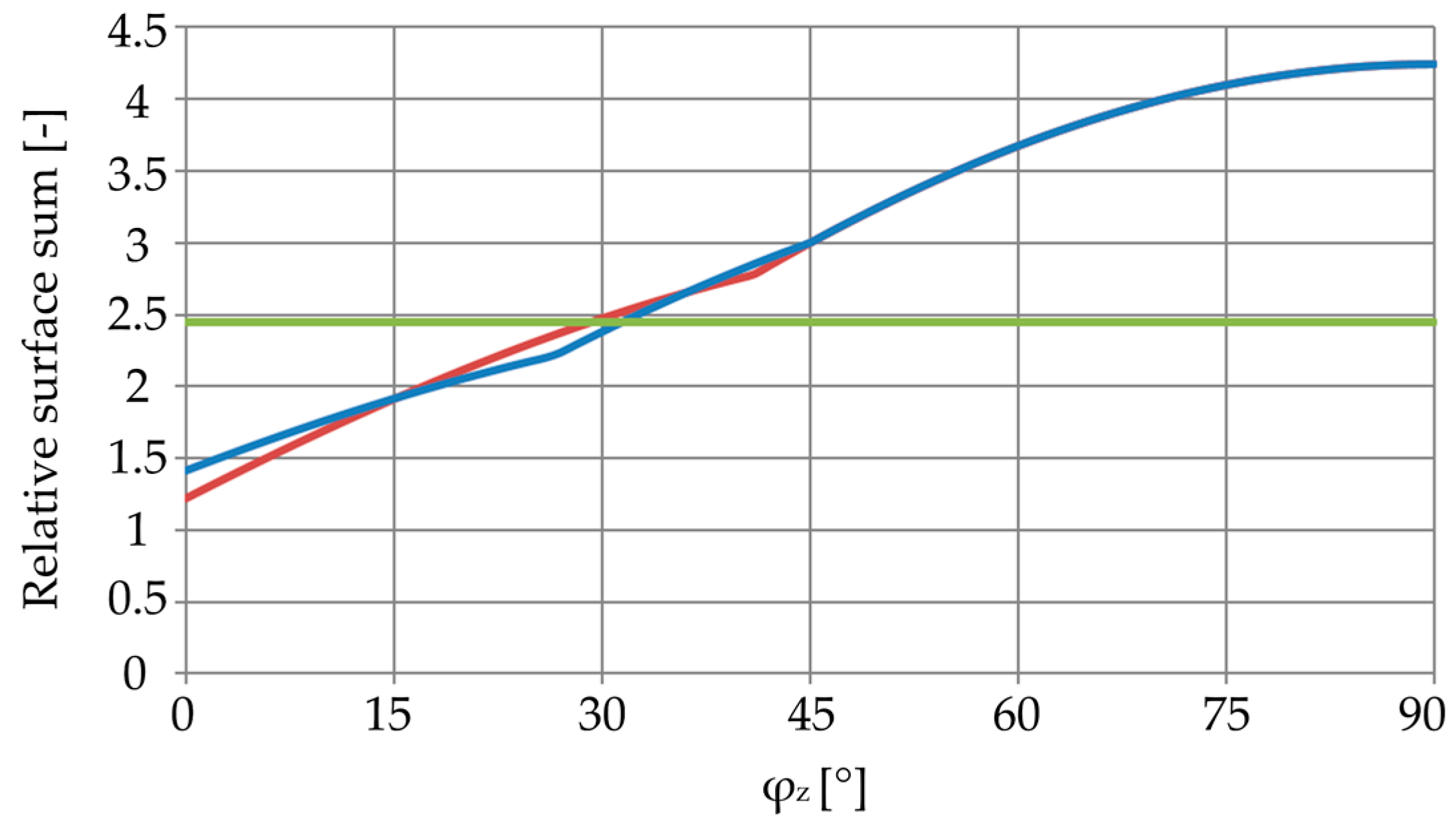
2. Free Space Optic (FSO) Receiver Design

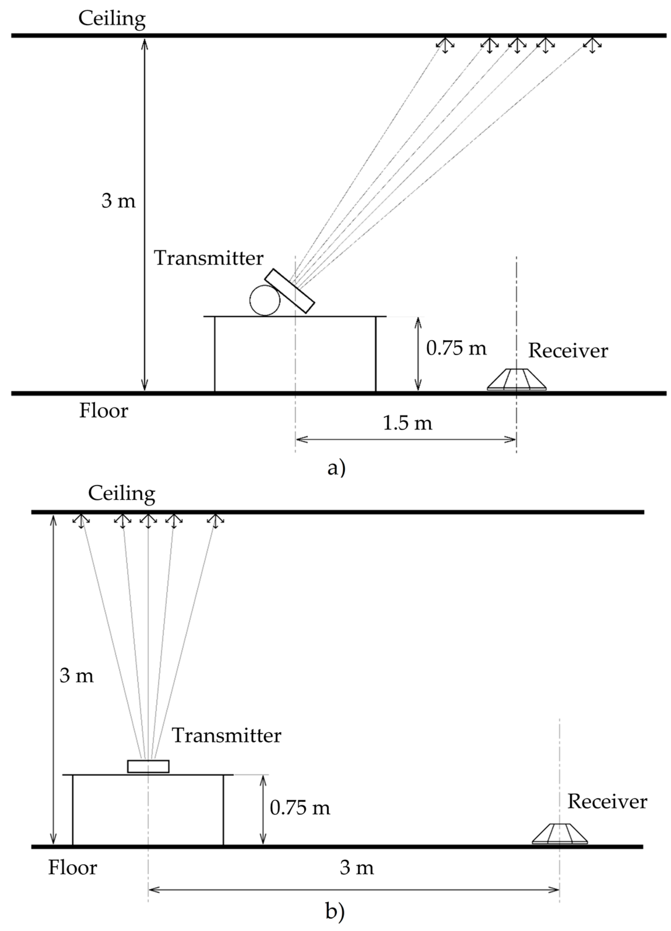
2.1. Receiver and Transmitter Parameters

The described FSO receiver was designed and assembled with the aim of providing the highest signal sensitivity and largest communication radius. It was planned mainly for interior use with multipath signal propagation. However, such optical channel properties might lead to a lower transfer frequency. Multipath light propagation loads the optical receiver input with unwanted jitter. Its size depends on the maximum path length difference between straight and mirrored rays. In contrast, the presence of many reflections enhances the SNR, as shown in Equation (7), and justifies the use of parallel amplifier topology. Another assumption is that the receiver has full mobility and responds to the whole hemisphere. As interior areas have humans present, the selected optical source spectrum was short wave infrared (SWIR), and the background light level was considered high.
To generate many useful light signal reflections, the optical source, particularly light-emitting diode (LED), must be sufficiently powerful. Powerful LEDs are not a problem; the problem is rather high-speed and high-powered LEDs. The solution is either an array of many LEDs with lower emitted power and excellent transfer frequency or a single luminophore free power LED with high emitted power and high transfer frequency. To record the measurements, an optical transmitter with one power LED VSMY99445 (Vishay, Malvern, PA, USA, 2015) by Vishay was used. Its peak wavelength is between 920 and 960 nm. Its radiant intensity reaches the level of 500 mW⋅sr-1 and a total radiant power of 935 mW. Both these values are achievable with a forward current of 1 A. Its beam allows switching between 0 A and 1 A currents with 15 ns and 18 ns rise and fall times, respectively. The LED driver was built as a high current, high frequency source. The tandem driver and the power LED can deliver a pulse train with a data speed as high as 10 Mbit·s−1.

2.2. FSO Receiver Bandwidth

The bandwidth is determined by the desired communication speed and the coding used. Thus far, no reference about the chosen encoding scheme has been given in this study. Due to multipath light signal propagation, simple encoding schemes are more reliable than complex schemes. Data are transferred by on/off keying related to light intensity modulation. Even though many good encoding schemes are available, the well-known phase encoding (PE) scheme, sometimes called “Manchester” encoding, was selected for the following reasons: balance of low and high symbols removing the DC part, resynchronization capability at the receiving end, and high noise immunity. Many other integrated solutions that facilitate PE implementation on the communication chain are available on the market, including devices such as HD-6409 by Intersil (Intersil, Milpitas, CA, USA, 2015) or DP8391 (alternatively DP83910A) by National Semiconductor (National Semiconductor, Santa Clara, CA, USA, 1995). With respect to bit error rate (BER) testing, the device used must maintain data transfer even with error symbols passing. Please note that this is not a usual process. For example, this is not the case with the HD-6409 device. The DP83910A device was ultimately selected as the best candidate. It possesses an analogue phase-locked loop (PLL) that allows the highest frequency range of the transferred data. It was built for a 10 Mbit·s−1 transfer speed but maintains functionality even for a 2 Mbit·s−1 transfer speed, which is an advantage because it broadens the testing capability and includes slower equipment.
By knowing the speed of the transmitter, PE codec hardware and the spectral density of the PE scheme [30], calculating the demanded receiver bandwidth, or more precisely, the receiver’s low and high cut-off frequencies, is not complicated. Even though both transmitter and PE codec hardware can transfer at speeds as high as 10 Mbit·s−1, some space remained, and the maximum lowered to a transfer speed of 2 Mbit·s−1. Based on this, the receiver’s low and high cut-off frequencies were 100 kHz and 1.5 MHz, respectively. Please note that the high cut-off frequency follows the rule of optimal filtering. This means that the PE spectral density high frequency decline starting at ¾ fbit may be approximated by the first order low pass filter roll-off, expressed as the number fh = ¾ fbit = ¾ 2 × 106 = 1.5 MHz. The low cut-off frequency of fl = 100 kHz was determined from BER measurements on the 2 Mbit·s-1 data stream.

2.3. Selecting a Suitable Photodetector

Many types of photodetectors exist. In terms of dynamic parameters, photodiodes or avalanche photodiodes are best suited for the proposed receiver. The latter include internal amplification. Generally, ordinary photodiodes and avalanche photodiodes use a simple PN junction and are quick enough only for visible light wavelengths. For the near infrared spectrum and high cut-off frequencies, PIN photodiodes and NPIP avalanche photodiodes have been developed.
Another consideration involves the internal amplification and conditions for using avalanche photodiodes. Internal amplification cannot improve the signal to noise ratio SNRin in the optical part, as in Equation (1). The input useful signal and input noise are both amplified in the same manner. Internal amplification is afflicted with its own noise, which increases with the magnitude of amplification. Internal amplification is therefore kept low and set only to a necessary magnitude that ensures that the photodetector noise current inPD is triple the follow-up amplifier noise current inA. Mathematically written:
i n P D 3 i n A       [ A ] .
Equation (19) requires commentary. First, the photodetector noise current inPD depends not only on the photodetector amplification magnitude but also on the photodetector background light level. Second, the internal amplification photodetector is unnecessary if the ordinary photodetector noise current inPD exceeds the noise current inA of the follow-up amplifier. It is obvious that the photodetector environmental conditions, particularly background light level, are important. The discussed FSO receiver’s high background light levels means that Equation (19) is fulfilled even with ordinary PIN photodiodes.
The decision above is not yet complete. It is also necessary to choose between PIN photodiodes with small active area and high cut-off frequency or PIN photodiodes with large active area and low cut-off frequency. Because the sensitivity of any photodetector is proportional to its active area and because a high communication radius depends not only on power LEDs but also on high sensitivity photodetectors, the latter PIN photodiodes are the best option. The typical representatives are BPW34 (Vishay, Malvern, PA, USA, 2011) or BP104F (Vishay, Malvern, PA, USA, 2011) devices. They were not selected randomly. BPW34 or BP104F are inexpensive and readily available. Compared with each other, neither have any large differences in peak sensitivity wavelength, rise and fall times, etc. An exception is the spectral bandwidth range. According to their datasheets, BPW34 is a wide spectral bandwidth photodiode covering wavelengths from 430 to 1100 nm, whereas BP104F is a narrow spectral bandwidth photodiode covering wavelengths from 800 to 1100 nm.
The spectral bandwidth range plays an important role during photodiode noise current inPD optimization. It is expressed as follows:
i n P D = J 2 ( f ) ¯ B         [ A ] ,
where B = fhfl is the useful signal bandwidth, and the photodiode noise power current spectral density is given by the well-known Schottky equation:
J 2 ( f ) ¯ = 2 q I 0         [ A 2 Hz 1 ] ,
where q is the electron charge and I0 is the dark current of the photodiode. From Equation (21), only quantity I0 remains which may be tuned by the user. The dark current I0 has three components: Idg (darkness generation current induced by phonons), Idb (darkness background current induced by far infrared /FIR/ photons), and finally Ipb (photocurrent background induced by near infrared /NIR/ and visible light photons). Written mathematically [1]:
I 0 = I d g + I d b + I p b         [ A ] .
The magnitudes of currents vary according to the application, and usually only one of these currents becomes dominant. A high background light level makes the Ipb current greater than the others. In an NIR photodetector and NIR application, Idb is almost zero (Idb = 72.97 × 10⁻²¹ A for BPW34 and Idb = 47.09 × 10⁻²¹ A for BP104F), and Idg is negligible (Idg = 2 nA, according to the datasheets of both photodiodes). The result is that the dark current I0 is determined only by Ipb. The total Ipb current can be found from the relative spectral sensitivity curve integration. Please note that the narrower spectral bandwidth range has a lower current Ipb and lower current noise inPD. Comparing the BPW34 and BP104F photodiodes, only the BP104F photodiode ensures lower Ipb currents and lower current noise inPD. Lower BP104F currents were confirmed by measurements for several types of illumination sources, shown in Table 1. The true Idg currents are also provided, confirming there is no better choice than the BP104F photodiode.
With respect to the best photodiode dynamics, a photoconductive regime was selected. This means that the photodiode was biased in reverse with as high a photodiode voltage UPD as permitted.

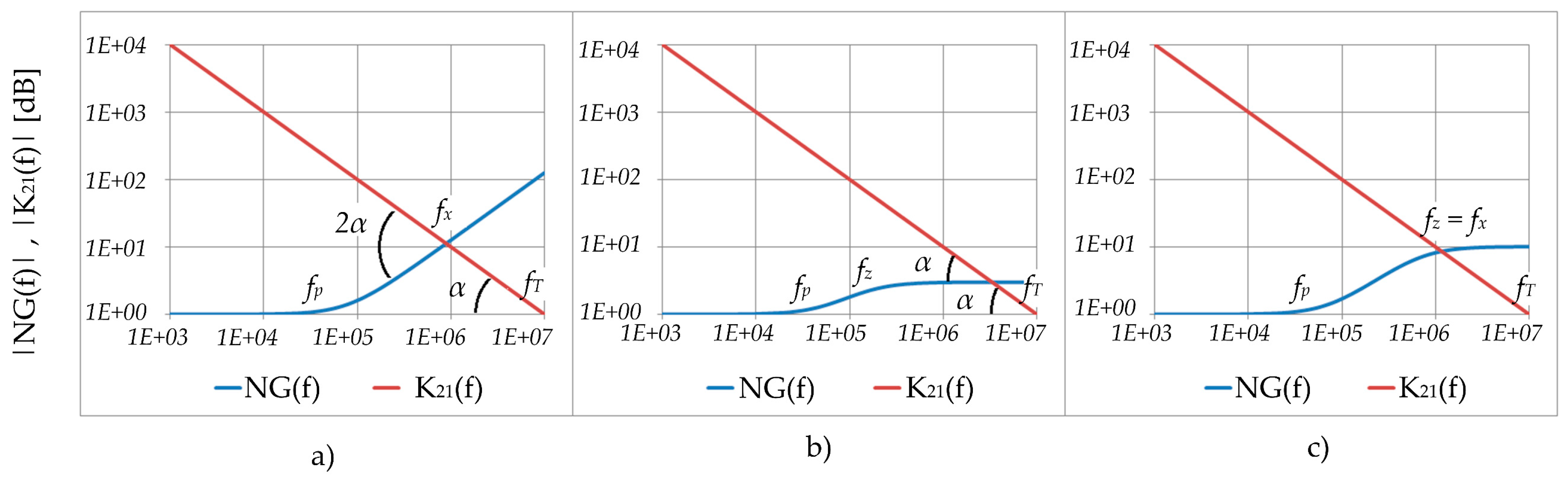
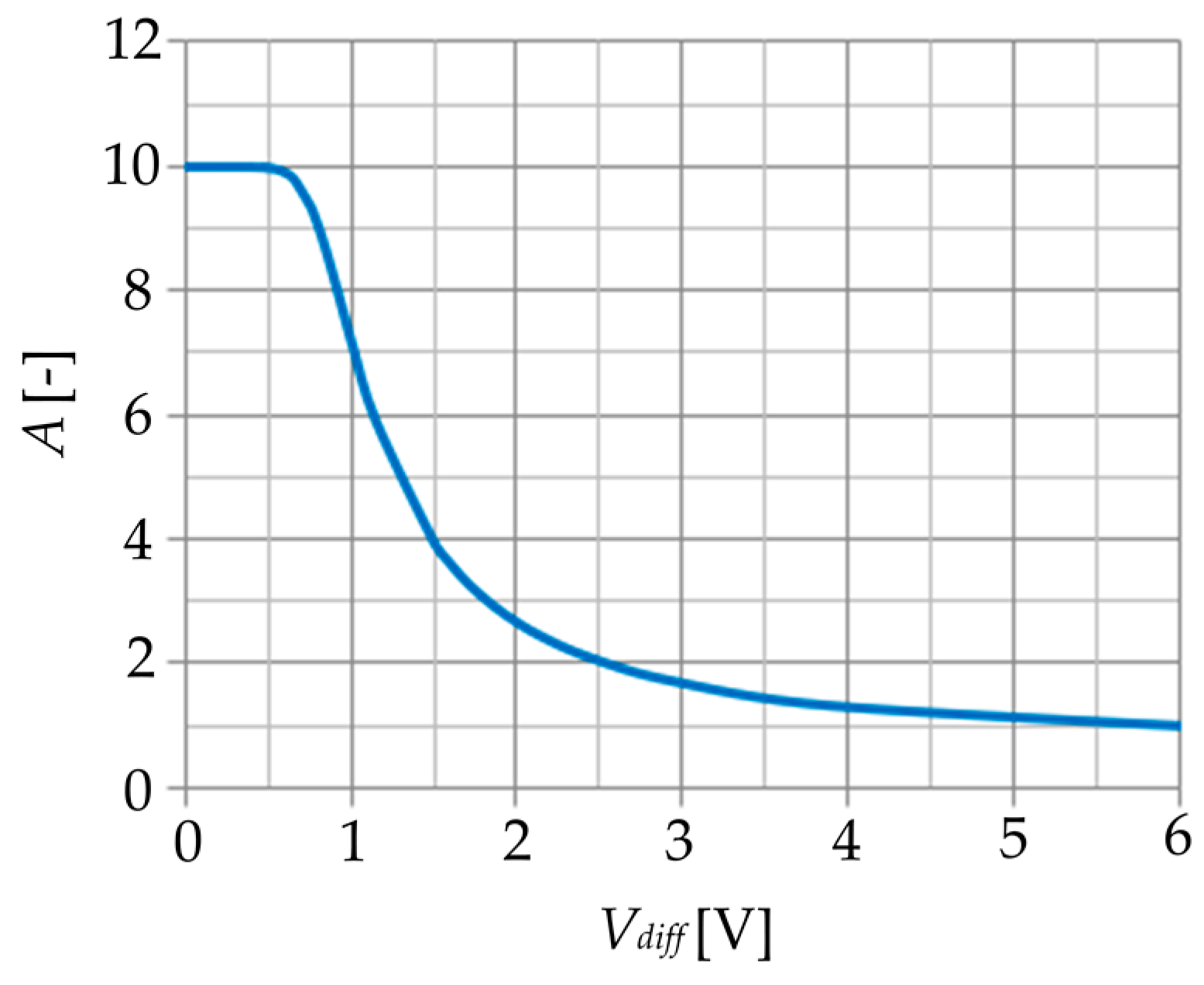
2.4. Selecting a Suitable Follow-Up Amplifier

Numerous aspects do not allow the application of all the design rules, which lead to the brief description of a suitable follow-up amplifier. However, we attempt to provide a description by citing other literature references.
Only the photodetector and the follow-up amplifier create the first receiver stage. Hence, their amplification should be as high as possible to eliminate noise in successive stages. They are derived in, for example, Zalud, V. et al. [31]. This first stage is usually called a PDA (photodetector assembly).
Another choice concerns amplifier topology: either direct or feedback topology, shown in Figure 6a,b, respectively. The names of components are as follows: PD is the photodiode, Ups is the power supply voltage, Cps is power supply decoupling capacitance, and RL is load resistance. For variant (a), the amplifier input impedance Za is not expressed and is covered by resistance RL. Similarly, for variant (b), the resistance RL is not expressed and is covered by feedback impedance Zfb. For direct topology, the K21 box is a bipolar or FET transistor; for feedback topology, it is a bipolar or FET operational amplifier. Due to the low noise requirements, any simple design is suitable. The direct amplifier topology (a) should be the best option, but it has many limitations [1]. The feedback amplifier topology, shown in Figure 6b, creates stability questions due to back feeding.
The noise model of the PDA is the same for both circuit diagrams (Figure 6a,b). It has been proven that back feeding cannot change the signal to noise ratio of a PDA [1]. The noise model showing a photodiode and follow-up amplifier with their passive network components is shown in Figure 6c. In the photodiode, Ip is the useful signal photocurrent, 2qI0 is the photodiode noise current density, and Rp and Cp are internal photodiode resistance and capacitance, respectively. In the amplifier, Ra and Ca are amplifier input resistance and capacitance, respectively (previously included in Za); 2qIa is the amplifier input noise current density; 4kT (Ψ/G) ω2Cin2 is the amplifier output noise current density calculated for the amplifier input; Gu1 is the amplifier useful signal output current; and Rfb and Cfb are feedback (load) resistance and capacitance, respectively (previously included in Zfb). The stray capacitances (e.g., the PCB capacitance) are not introduced explicitly and may be included in Cfb. Since all components are in parallel, the input impedance Zin may be expressed as:
1 Z i n = 1 R i n + j ω C i n = ( 1 R p + 1 R a + 1 R f b ) + j ω ( C p + C a + C f b )         [ S ] .
The whole PDA noise power current spectral density is given by the equation:
J P D A 2 ¯ = F N f + 2 q I 0 + 2 q I a + 4 k T R i n + 4 k T ψ G ω 2 C i n 2         [ A 2 Hz 1 ] .
where FN/f is the flicker noise of the photodiode and amplifier; 2qI0 and 2qIa are the shot noises of the photodiode and amplifier, respectively; 4kT/Rin is the thermal noise of the total input resistance Rin according to Equation (23) and 4kT (Ψ/G) ω2Cin2 is the amplifier output noise current density calculated for the amplifier input. This current density can also be expressed in shorter form as en2ω2Cin2. Since the shot and thermal noises are independent of frequency, they are white noise and may be substituted by element 2 q I n = 2 q I 0 + 2 q I a + 4 k T / R i n . It is useful to unify Equation (24):
Ξ ( f ) = J P D A 2 ( f ) ¯ 2 q I n = F N 2 q I n 1 f + 1 + ( 2 π C i n ) 2 e n 2 ¯ 2 q I n f 2 = f l o w N f + 1 + f 2 f h i g h N 2       [ / ] .
From Equation (25), the low cut-off and the high cut-off frequencies of white noise will be:
f l o w N = F N 2 q I n         [ Hz ] ,       f h i g h N = 2 q I n 2 π C i n e n ¯         [ Hz ] .
After preparation of the above, the low frequency PDA and the high frequency PDA can be classified and optimized. Because the described FSO receiver is a high frequency PDA (with high cut-off frequency fh = 1.5 MHz), only the latter optimization is discussed.
High frequency DPA noise optimization is performed with respect to the en2ω2Cin2 element, which becomes dominant. An amplifier with the lowest input voltage noise en and the lowest input capacitance Ca (determining Cin) is necessary. The other conditions are as follows:
4 k T R i n e n 2 ¯ ω h 2 C i n 2                 R i n 4 k T e n 2 ¯ ω h 2 C i n 2
4 k T R i n = 2 q I a                 I a = 4 k T 2 q R i n = 4 U T 2 R i n = 2 U T R i n
1 2 π R i n C i n f h  
where Rin in Equation (28) is calculated from Equation (27). Equation (29) serves only to verify that the high cut-off frequency of PDA fh is fulfilled. If not, high frequency amplification loss should be compensated by a separate corrective circuit. An operational amplifier whose gain is big enough can cancel this loss and maintain the stability of the amplification up to frequency fx (see below).
Even though much has been discussed about follow-up amplifier design, bipolar or unipolar transistor use should be defined. Generally, the sources of noise in unipolar transistors are mutually independent and may be optimized much more easily. This is not the case for bipolar transistors, in which the lowering of input noise is linked to the lowering of input current, which further leads to lower transistor gain and higher output noise effects. Because of negligible FET input currents, they are the best choice in most cases. Trishenkov, M.A. [1] provides more details.
The final point concerns the FET itself. Based on the recommendations above, a careful designer looks for the lowest voltage noise en and the lowest input capacitance Ca in a discrete FET or the input FET operational amplifier. However, it has been proven that FET voltage noise en and FET input capacitance Ca are reciprocal [1]: the lower the voltage noise en, the higher the input capacitance Ca and vice versa. In other words, capacitive matching is needed:
C a = C p .
For completeness, stability is required. Figure 7 is helpful with this explanation.
The blue line is the noise gain NG defined, for example, by Jung, W. [32]; the red line is the follow-up amplifier K21 high frequency roll-off. System stability is determined by the intersection angle between the blue and red lines. If the angle is equal to the red line and the horizontal axis angle, the system is stable; if it is greater, the system is unstable.
The pool frequency fp of the amplifier passive network is defined as:
f p = 1 2 π R i n C i n         [ Hz ] .
The zero frequency is determined only by feedback impedance:
f z = 1 2 π R f b C f b         [ Hz ] .
The transit frequency fT is determined by the amplifier roll-off and the 0 dB level intersection, which is also known as the gain-bandwidth product of an operational amplifier (GBW). Finally, the amplifier roll-off and noise gain also intersect, whose frequency fx is:
f x = f p f T   [ Hz ] .
The frequency fx should equal fh, which is the high cut-off frequency of the PDA. For the FSO receiver discussed, this is fh = fx = 1.5 MHz.
Based on the theoretical analysis, it is now possible to proceed with the calculation of the specific components. The suitable low input voltage noise en and capacitance Ca operational amplifiers are listed in Table 2.
In Table 2, input capacitance Ca, input voltage noise en, and transit frequency fT are typical values seen in operational amplifier datasheets. Total input capacitance Cin is the sum of the BP104F photodiode typical capacitance Cp = 16 pF (10 V reverse biased), stray capacitance Cs = 3 pF and the operational amplifier input capacitance Ca. The frequency fx was matched to the PDA’s high cut-off frequency fh (fx = fh = 1.5 MHz). Due to the high frequency PDA, high cut-off frequency fh is the same as the zero frequency fz, shown in Figure 7c, fz = fh = 1.5 MHz. The amplifier output noise current density en2ωx2Cin2 was determined by calculation. The Rin and Ia conditions are derived from Equations (27) and (28), respectively. Similarly, pool frequency fp, feedback resistance Rfb (which determines Rin), and feedback capacitance Cfb are derived from Equations (33), (31) and (32), respectively. Based on Table 2 and our calculations, we concluded the following: the OPA602BP (Texas Instruments, Dallas, TX, USA, 2002) device does not fulfil the capacitance matching conditions (Ca = 1 pF, Cp = 16 pF, Ca << Cp); input voltage noise en is the highest, with the small input capacitance Ca being eliminated by the enormous Cp capacitance. This was confirmed by the highest en2ωx2Cin2 element. Therefore, the OPA602BP device is not suitable for the FSO receiver design. The OP27G (Analog Devices, Norwood, MA, USA, 2015) and the OPA627BP (Texas Instruments, Dallas, TX, USA, 2015) devices have much lower en2ωx2Cin2 values. OP27G appears to be the best for the application. For a stable feedback loop, the resistance Rfb must be lower than the required minimum resistance Rin, Rfb < Rin, which destroys the good noise parameters of an operational amplifier. Neither OPA602BP nor OP27G meet with the PDA’s requirements. The opposite relation Rfb > Rin is only provided by the OPA627BP device, in which the en2ωx2Cin2 value is three times higher and a high resistance Rfb keeps thermal noise low, leading to high stage transimpedance. Therefore, the OPA627BP is the only device suitable for the low noise PDA requirements.
The capacitance Cfb keeps the amplifier feedback stable, bending the noise gain NG at the zero frequency fz (Figure 7). It is also responsible for the shape of the PDA closed loop amplitude frequency characteristic around the high cut-off frequency point fh. No overshoot should exist in the frequency characteristic for a well-compensated PDA. If this is the case, the frequency characteristic is closer to the first order declining asymptote from the left, and high frequency noises are kept to their minimum. All other cases are undesirable. Even a small overshoot brings the frequency characteristic closer toward the first order declining asymptote from the right, and the PDA output is loaded with excessively high frequency noise. The capacitance Cfb is therefore usually set with a variable capacitor according to the frequency or time domain measurements.
Time domain measurements are much easier to perform. The required instruments are an oscilloscope and an optical fast leading and trailing edge pulse generator. The PDA output voltage waveform should be as close as possible to the optical pulse generator waveform and free of overshoots. Once the feedback capacitance Cfb has been set, neither photodiode reverse bias nor any other items can be changed.
We compared the amplifier input current Ia and the dark current I0, as in the condition in Equation (19). With the maximal allowed amplifier current Ia = 5.47 μA, the condition in Equation (19) is fulfilled under incandescent lamp illumination. Under daylight, the currents are rather the same, which is still acceptable.

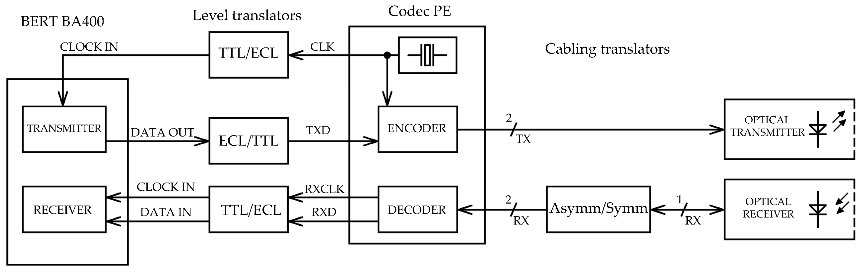
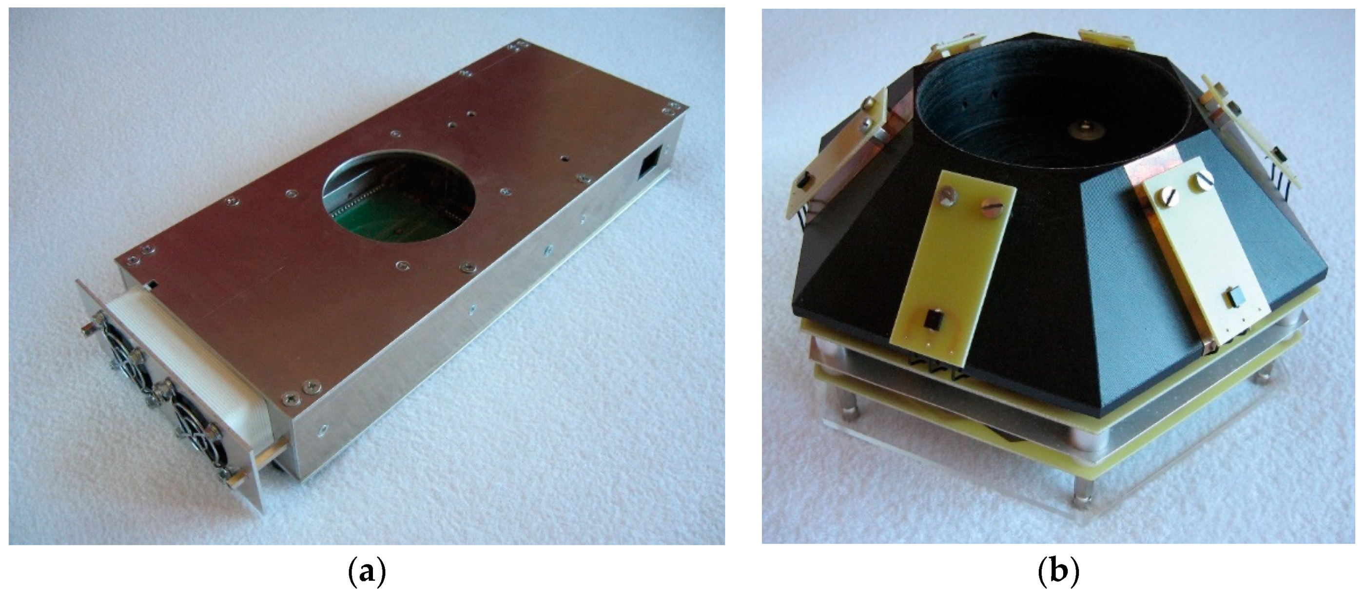
3. FSO Receiver Assembly

The discussed FSO receiver consists of several blocks (Figure 8). Given s photodetectors used, there are s follow-up amplifiers, in other words, s PDAs. The PDA count is determined by the truncated pyramid wall count. Here, s = 6. PDA amplification is kept constant with well-defined circuit parameters and feasible noise optimization. PDA outputs are summed and amplified with a variable gain amplifier (VGA). Due to the FSO receiver’s mobility, the VGA block is essential. The input optical useful signal power does not have the same value over time; it changes with the distance of the optical transmitter from the receiver and the optical channel’s parameters. The receiver’s gain must therefore be permanently adjusted, otherwise either a lack or excess of the receiver’s output signal power would occur. A lack of power would mean loss of the connection, whereas an excess would deteriorate the signal to noise ratio. To provide correct and invariable output signal power, the power is measured by the detector block and compared to the reference voltage block Vref. The optimal gain value of the VGA is set according to the obtained voltage difference Vdiff.

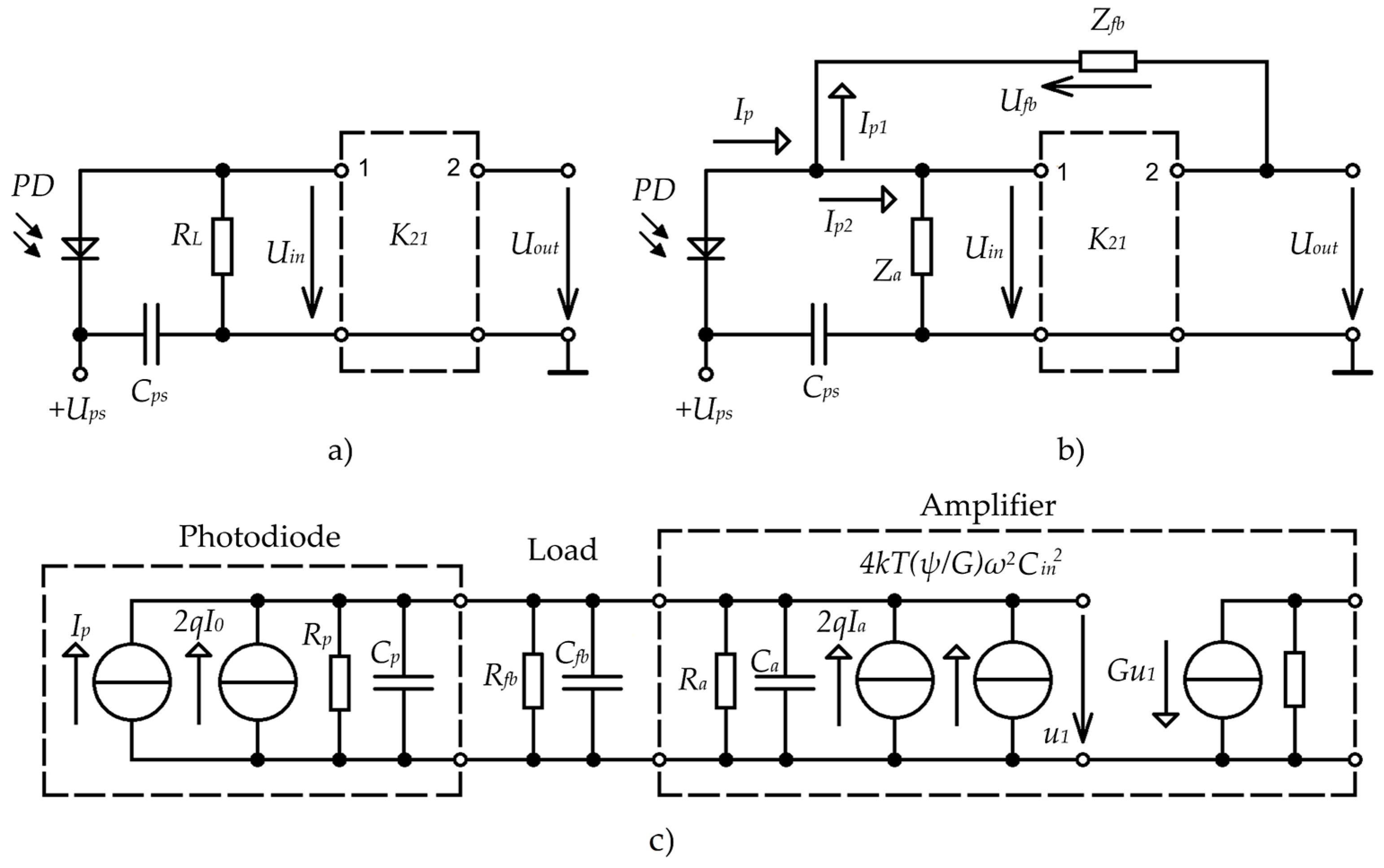
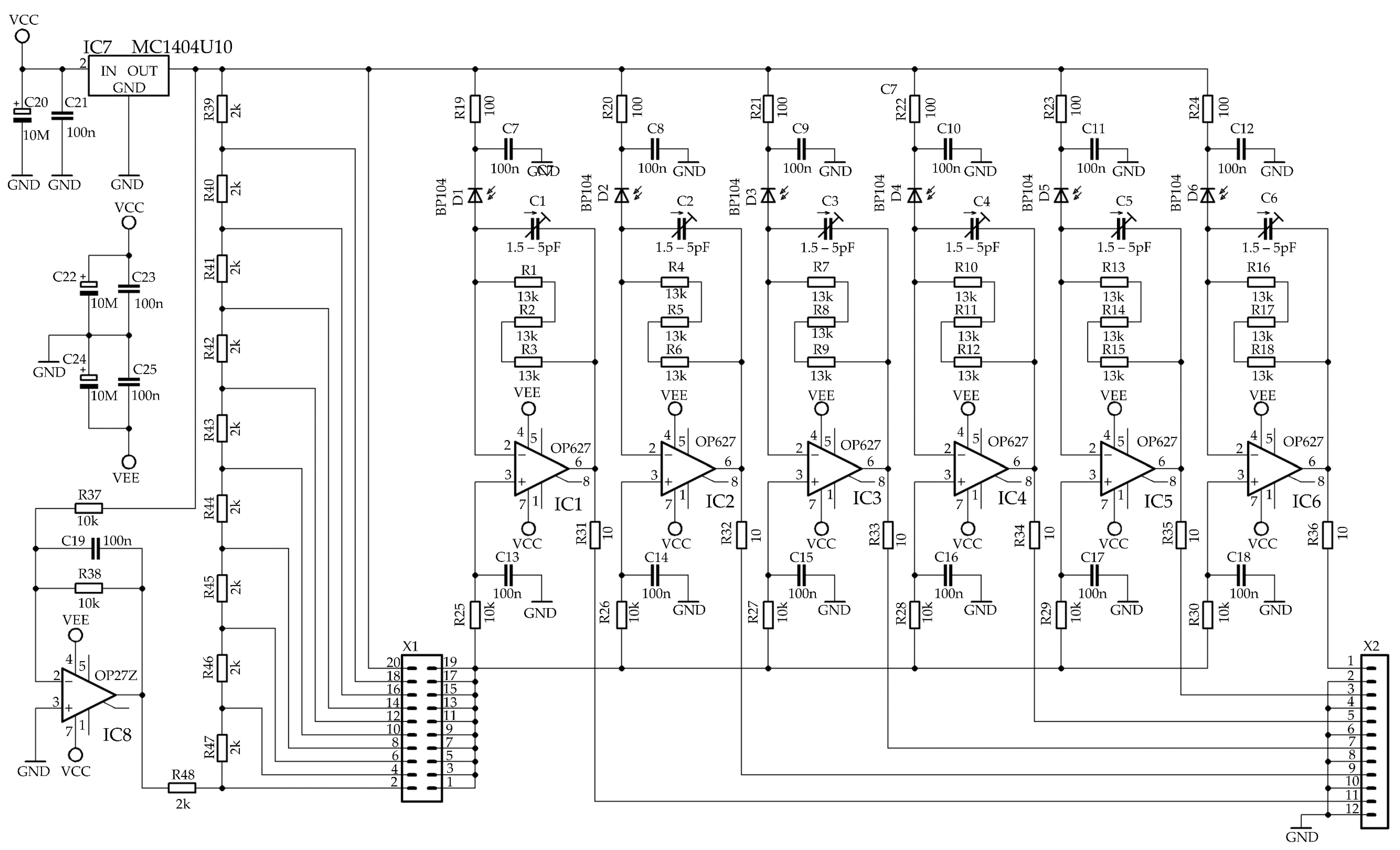
Detailed Circuit Diagram of the FSO Receiver

Since this paper deals mainly with PDA design, only a PDAs circuit diagram is provided. The remaining blocks are rather universal and may be substituted by any circuit that fulfils their function. Notably, low noise circuits are required.
A detailed circuit diagram is shown in Figure 9. At the right of Figure 9 are six PDA cells, each including a photodiode BP104F (D1–D6), operational amplifier OPA627BP (IC1–IC6), feedback resistors 3 × 13 kΩ (R1–R18), and feedback variable capacitor 1.5–5 pF (C1–C6). The feedback resistance and capacitance values are listed in Table 2. No standard series 42 kΩ resistor was available, so it was replaced by the closest lower value resistor of 39 kΩ. Three 13 kΩ resistors were used in order to minimize intrinsic terminal capacitance and PCB stray capacitance. This was necessary because of the low predicted capacitance Cfb = 2.53 pF and a non-zero capacitance of 1.5 pF in the variable capacitor. At the left of Figure 9 are the voltage reference MC1404U10 (ON Semiconductor, Phoenix, AZ, USA, 2006) (IC7) and reference voltage inverter OP27 (IC8). Both are low noise devices.
The next step included innovations to reduce noise to a minimum and for uncorrelated elementary PDAs. The photodiode cathode voltages were fixed, whereas the anode voltages varied according to the resistive divider branch selection (R39–R48). There is no variable resistor because of excessive noise coming from its wiper and resistive lane connection. Even though the maximum allowed reverse voltage was recommended, it decreases exactly when higher flicker noise photodiodes are encountered [1]. To keep the PDA noise uncorrelated, the photodiodes were fed through low-pass filters (R19–R30, C7–C18). Capacitors C13–C18 also eliminate noise currents in the operational amplifier noninverting inputs. Resistors R31–R36 separate possible external capacitive loads and operational amplifier outputs. As a result, the stability of the operational amplifiers is independent of the load conditions and cabling. The PDA outputs are summed in the next stage (VGA circuit).

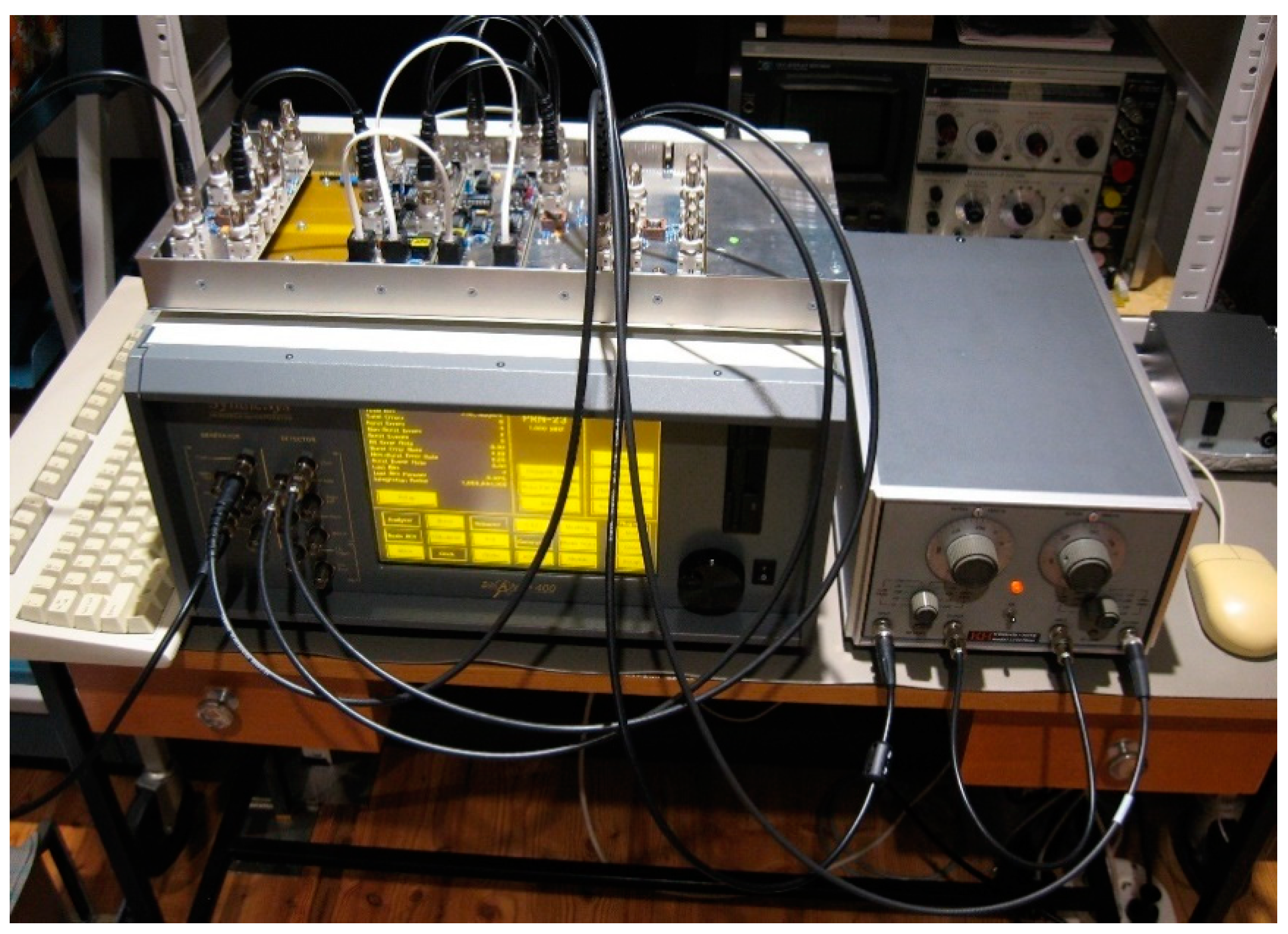
4. FSO Receiver Measurements

The FSO multiple photodetector receiver noise parameters were measured indirectly by evaluating the bit error rate (BER) parameters. The measurement block diagram is depicted in Figure 10. A BA400 (SyntheSys Research, Menlo Park, CA, USA, 1992) tester was used to create the BER evaluation core. The level translators matched the BER tester ECL and codec PE TTL interfaces. As stated above, the PE codec employs the DP83910A device. Because of different asymmetrical and symmetrical port architectures, a cabling translator was added. The optical transmitter equipped with power LED VSMY99445 is shown in Figure 11a. The assembled FSO multiple photodetector receiver described here is shown in Figure 11b. Other equipment used for BER measurement is shown in Figure 12.
All measurements were performed at night with a stable diffusion LED illumination of 400 lx. The BER measurements operated over a 2 Mbit·s−1 data stream and x23 + x5 + 1 (n = 23) pseudorandom sequence. The calculations between the BER and the SNR parameters were provided by the “erfc” Excel function according to the following definition [33,34]:
B E R = 1 2 erfc ( S N R 2 2 )   [ / ] .
The BER measurement of the FSO multiple photodetector receiver was differentiated by the number of the actively operating photodetectors. As the occurrence of errors and the measured BER values are random, a higher number of measurements was required. The volume of the transferred data was always at least 10 times higher than the expected BER reciprocal value. Table 3 shows the measured data.
It follows from the BER measurements that the change in noise parameters from only one to all six actively operating photodetectors was too large. The first short optical route allowed BER measurements of a lower number of actively operating photodetectors, whereas, for a higher number of actively operating photodetectors, the BER measurements were zero. However, the second-long optical route permitted BER measurements with a higher number of actively operating photodetectors, whereas for a lower number of actively operating photodetectors, it was difficult to establish a link.
Notably, our goal was to focus on only one optical route. The experiences were as follows:
When using short optical route, the BER measurements were possible for one, two and three actively operating photodetectors. However, the BER measurement for all six actively operating photodetectors was zero for time in units of hours. As can be calculated from the last row of Table 3, the BER difference between only one and all six actively operating photodetectors is over five orders. Since the estimated BER value for all six actively operating photodetectors and short route would be between 10−10 and 10−11, the time needed for measurements would be huge, reaching around 140 h (almost one week). The total measurement time would have to be extended at least to one month because several measurements are required.
The long optical route was successfully tested for only three or six actively operating photodetectors. For lower numbers of actively operating photodetectors, there was problem with resynchronization at the receiver part of the BER tester Synthesys BA400. The results improved using a simpler x7 + x + 1 (n = 7) pseudorandom sequence or with the only one word (16 bits) repeated over and over again. However, the measurement was still unstable and synchronization was frequently lost. Even if the synchronization succeeded, the measured values would not be accurate due to the short data string and the presence of harmonic components in the spectrum of such testing signal. For the above reasons, two optical routes had to be used for measurement.
The short optical route from the transmitter to the receiver was created via the only main reflective surface: the room’s ceiling (Figure 13a). The transmitter was deflected to provide reflection just above the receiver. The plaster’s natural scattering ability was beneficial. The distance between the transmitter and the receiver on the floor was 1.5 m. Room height was 3 m and the floorplan dimensions were 6 m × 3.5 m. The transmitter and receiver were positioned so that no line of sight existed between them.
The long optical route was established via numerous reflections from the ceiling and walls. This time, the transmitter had no deflections, as shown in Figure 13b. The distance between the transmitter and the receiver on the floor was doubled to 3 m. The room height was again 3 m, and similarly, the floorplan dimensions were 6 × 3.5 m. No line of sight was permitted between the transmitter and the receiver. Under these conditions, signal coverage was almost uniform.
The last row in Table 3 is related to the long optical route SNR values and shows the calculated SNR values for the two actively operating photodetectors via the short optical route, i.e., 17.85 − (21.45 − 18.19) = 14.59 dB, and similarly for only one actively operating photodetector, i.e., 17.85 − (21.45 − 17.91) = 14.31 dB. If a link could have been established for only one actively operating photodetector via the long optical route, the BER value would have been very high, achieving 4.63 × 10⁻³. The SNR difference between only one and all six actively operating photodetectors was 6.41 dB, which is close to the theoretical value of 4.8 dB calculated above. As a reminder, the theoretical value of 4.8 dB was calculated as the SNR difference between only one and all six operating photodetectors with uniform signal coverage. In other words, this calculated difference covered only photodetector inherent noise suppression. The better result of 6.41 dB appears to be an inaccuracy arising from the unequal short and long optical routes. However, useful signal and noise processing differs, and no tool exists to precisely handle noise. Adding signals from the photodetectors means decreasing instead of increasing peak-to-peak total noise values. The measured result of 6.41 dB encourages more investigation with perhaps the same or more photodetector receivers.
The active operation of only one or two photodetectors does not differ much in the BER or SNR parameters. Compared to more photodetectors, the situation with two actively operating photodetectors was exceptional due to the presence of error bursts. This can be explained by the higher probability of both noise voltages meeting in phase to produce noise spikes much higher than standard background noise. These peaks prevail in amplitude and in time, leading to longer data training dropouts.
We examined the results of the comparison of the BER parameters with three or six operating photodetectors. The difference was more than three orders higher, which is considerable during mainly data transfer. Many papers in initial studies mention an optical channel with the FOV of the photodetectors not overlapping or only slightly overlapping. According to the BP104F photodiode datasheet, its FOV is 130°. With the FOV of photodiodes not overlapping, three BP104F photodiodes should be enough for receiving. Highly overlapped FOVs in six operating photodetectors BP104F would have no adverse impact, and instead provide a benefit. Strongly overlapped FOVs lead to parallel information processing and eliminate the uncorrelated noise of photodetectors and follow-up amplifiers (PDAs).
The operation of all six photodetectors in a multipath light signal propagation environment provides a high communication radius at very low BER. This is proved by the measured average BER value of 2.72 × 10⁻⁸ at ray trajectories equal to or longer than 6 m with a data stream as high as 2 Mbit·s−1.
When evaluating multiple photodetector receivers, no phenomenon concerning the addition of photodetectors noise can be ignored. The block diagram in Figure 8, showing a peak-to-peak voltage detector, voltage reference Vref, comparator, variable gain amplifier, and its control voltage Vdiff, can be helpful in describing this. Adding noise increases its resultant power according to RMS. Peak-to-peak noise values are described by the noise power distribution function. The higher the noise RMS value, the higher the peak-to-peak values. However, we observed a difference in the photodetectors adding noise, which can be seen in Table 4 and from the graph in Figure 14.
Figure 14 shows that higher voltages Vdiff reduce VGA gain and vice versa. This means that an empty signal channel makes the Vdiff lowest and the VGA gain highest; similarly, a full signal channel makes the Vdiff highest and VGA gain lowest. The channel may be filled with a useful signal or with noise. According to Table 4, increasing the number of operating photodetectors (without a useful signal) cleared the channel, which was an unexpected but positive result.

5. Conclusions

An FSO multiple photodetector receiver, using equal signal combining, was described in this paper. Instead of using additional optical elements, the receiver included six photodetectors providing omnidirectional receiving capability. We used the near infrared optical spectrum. Due to high background light levels, the receiver employed ordinary PIN photodiodes. The photodiodes were fixed to truncated pyramid walls; the walls and base were at an angle of 45°. The receiver was designed for interior use with multipath light signal propagation. The FOVs of the photodiodes were highly overlapped and covered one hemisphere. We discussed the separation of optical and electrical noise and demonstrated that highly overlapped FOVs eliminate electrical (PDAs) noise and are advantageous in environments with reflections or low optical noise. In other words, highly overlapped FOVs provide parallel information processing and additive noise suppression. To preserve this advantage, falling rays must be over a minimum angle of 32° with respect to the receiver’s base. The procedure used to derive the minimum angle was described and generalized for different photodiode holders. We continued with PIN photodiode selection and follow-up amplifier design. Feedback amplifier topology appeared best for the application. For the final PDAs, PIN photodiodes BP104F and DiFET operational amplifiers OPA627BP were selected. With respect to slower power LEDs, the optical receiver was designed for a 2 Mbit·s−1 data stream.
The FSO multiple photodetector receiver noise parameters were indirectly measured by evaluating the bit error rate (BER) parameters. The calculations between the BER and SNR parameters were performed with the erfc function in Excel. Measurements were differentiated by the number of actively operating photodetectors. All measurements confirmed our theoretical assumptions. The operation of all six photodetectors in a multipath light signal propagation environment provided an exceptional communication radius over 6 m at a low BER value of 2.72 × 10⁻⁸ with FOVs highly overlapped. By contrast, the operation of only three photodetectors failed, with a high BER value of 4.79 × 10⁻⁵ for the same configuration and FOVs only slightly overlapped.

Author Contributions

K.W. proposed the sensor system idea and designed the sensor. K.W. and J.N. edited the manuscript, also tested and validated the experiments and performed its final edits.

Funding

This article was supported by the Ministry of Education of the Czech Republic (Projects No. SP2019/67, SP2019/80, and SP2019/85). This research was partially supported by the Ministry of Education, Youth and Sports of the Czech Republic through Grant Project no. CZ.1.07/2.3.00/20.0217 within the framework of the Operation Programme Education for Competitiveness financed by the European Structural Funds and from the state budget of the Czech Republic. This article was also supported by the Ministry of the Interior of the Czech Republic within the projects Nos. VI20152020008 and VI2VS/444, as well as the Ministry of Industry and Trade of the Czech Republic within the project Nos. FV10396 and FV20581. It was also supported by the Grand Agency of the Czech Republic (project # 15-21547S) and the European Regional Development Fund in the Research Centre of Advanced Mechatronic Systems project, project number CZ.02.1.01/0.0/0.0/16_019/0000867 within the Operational Programme Research, Development and Education.

Conflicts of Interest

The authors declare no conflict of interest.

References

  1. Trishenkov, M.A. Detection of Low-Level Optical Signals: Photodetectors, Focal Plane Arrays and Systems; Solid-State Science and Technology Library; Springer: Basel, Switzerland, 1997; ISBN 0792346912. [Google Scholar]
  2. Puschell, J.; Bayse, R. High data rate ultraviolet communication systems for the tactical battlefield. In Proceedings of the Tactical Communications Conference, Fort Wayne, IN, USA, 24–26 April 1990; pp. 253–267. [Google Scholar]
  3. Majumdar, A. Non-Line-Of-Sight (NLOS) Ultraviolet and Indoor Free-Space Optical (FSO) Communications. In Advanced Free Space Optics (FSO); Springer: New York, NY, USA, 2015; pp. 177–202. [Google Scholar]
  4. Mcclintock, R.; Razeghi, M.; Tournie, E.; Haddadi, A.; Brown, G.J. Free-space optical communication using mid-infrared or solar-blind ultraviolet sources and detectors. In Proceedings of the SPIE, Quantum Sensing and Nanophotonic Devices IX, San Francisco, CA, USA, 22–26 January 2012. [Google Scholar]
  5. Hall, E.; Cao, Z.L. Omnidirectional Viewing using a Fish Eye Lens. In Proceedings of the SPIE, Bellingham, WA, USA, 22 January 1987; pp. 250–256. [Google Scholar]
  6. Iguchi, Y.; Yamaguchi, J. Omni-directional 3D measurement using double fish-eye stereo vision. In Proceedings of the IEEE 21st Korea-Japan Joint Workshop on Frontiers of Computer Vision, Mokpo, Korea, 28–30 January 2015; ISBN 978-1-4799-1720-4. [Google Scholar]
  7. Takeya, A.; Kuroda, T.; Nishiguchi, K.; Ichikawa, A. Omnidirectional vision system using two mirrors. In Proceedings of the SPIE, San Diego, CA, USA, 8 December 1998; pp. 250–256. [Google Scholar]
  8. Zhang, C.; Xu, J.; Xi, N.; Jia, Y.; Li, W. Development of an omni-directional 3D camera for robot navigation. In Proceedings of the IEEE/ASME International Conference on Advanced Intelligent Mechatronics, Kachsiung, Taiwan, 11–14 July 2012. [Google Scholar]
  9. Sooyeong, Y.; Ahuja, N. An omnidirectional stereo vision system using a single camera. In Proceedings of the ICPR, Hong Kong, China, 20–24 August 2006; pp. 861–865. [Google Scholar]
  10. Marsh, G.; Kahn, J.M. 50 Mb/s diffuse infrared free-space link using on-off keying with decision-feedback equalization. IEEE Photonics Technol. Lett. 1994, 6, 1268–1270. [Google Scholar] [CrossRef]
  11. Agrawal, N.; Davis, C.C. Design of free space optical omnidirectional transceivers for indoor applications using non-imaging optical devices. In Proceedings of the SPIE, Free-Space Laser Communications VIII, San Diego, CA, USA, 10–12 August 2008. [Google Scholar]
  12. Murshid, S.; Lovell, G.L.; Finch, M.F. Omnidirectional Free Space Optical Receiver Architecture. In Proceedings of the SPIE, Photonic Applications for Aerospace, Commercial, and Harsh Environments IV, Baltimore, MD, USA, 29 April–1 May 2013. [Google Scholar]
  13. Murshid, S.H.; Lovell, G.L.; Finch, M.F. Modeled and experimental results of a omnidirectional free-space optical receiver architecture. Opt. Eng. 2017, 56. [Google Scholar] [CrossRef]
  14. Burton, A.; Ghassemlooy, Z.; Rajbhandari, S.; Liaw, S.K. Design and analysis of an angular-segmented full-mobility visible light communications receiver. Trans. Emerg. Telecommun. Technol. 2014, 25, 591–599. [Google Scholar] [CrossRef]
  15. Jungnickel, V.; Forck, A.; Haustein, T.; Kruger, U.; Pohl, V.; von Helmolt, C. Electronic tracking for wireless infrared communications. IEEE Trans. Wirel. Commun. 2003, 2, 989–999. [Google Scholar] [CrossRef]
  16. Trisno, S.; Tzunh-Hsien, H.; Milner, S.D.; Davis, C.C. Theoretical and experimental characterization of omnidirectional optical links for free space optical communications. In Proceedings of the MILCOM, Monterey, CA, USA, 31 October–3 November 2004; pp. 1151–1157. [Google Scholar]
  17. Alqudah, Y.A.; Kavehrad, M. Optimum Order of Angle Diversity with Equal-Gain Combining Receivers for Broad-Band Indoor Optical Wireless Communications. IEEE Trans. Veh. Technol. 2004, 53, 94–105. [Google Scholar] [CrossRef]
  18. Farr, N.; Chave, A.D.; Freitag, L.; Preisig, J.; White, S.N.; Yoerger, D.; Sonnichsen, F. Optical modem technology for seafloor observatories. In Proceedings of the OCEANS, Washington, DC, USA, 17–23 September 2005. [Google Scholar]
  19. Liu, X.; Gong, C.; Li, S.; Xu, Z. Signal Characterization and Receiver Design for Visible Light Communication under Weak Illuminance. IEEE Commun. Lett. 2016, 20, 1349–1352. [Google Scholar] [CrossRef]
  20. Sundqvist, B.; Backstrom, G. Low noise and drift by parallel amplifiers. Rev. Sci. Instrum. 1975, 928–929. [Google Scholar] [CrossRef]
  21. Scandurra, G.; Giusi, G.; Ciofi, C. Multichannel Amplifier Topologies for High-Sensitivity and Reduced Measurement Time in Voltage Noise Measurements. IEEE Instrum. Meas. 2013, 62, 1145–1153. [Google Scholar] [CrossRef]
  22. Coloumbe, J.; Rossel, O.; Bernard, S.; Soulier, F.; Cathebras, G. A new shared-input amplifier architecture with enhanced noise-power efficiency for parallel biosignal recordings. In Proceedings of the IEEE International Symposium on Circuits and Systems, Seoul, Korea, 20–23 May 2012; pp. 846–849. [Google Scholar]
  23. Hausman, H. Modeling parallel amplifiers. In Proceedings of the IEEE International Conference on Microwaves, Communications, Antennas and Electronic Systems, Tel Aviv, Israel, 2–4 November 2015; pp. 1–5. [Google Scholar]
  24. Wahab, F.A.; Leong, T.K.; Zulkifli, H.; Ibrahim, M.I.B.; Talib, M.A.B.; Zamri, N.A.; Ibrahim, O.K. Multiple transmitters & receivers for free space optical communication link performance analysis. J. Telecommun. Electron. Comput. Eng. 2016, 8, 29–32. [Google Scholar]
  25. Noor, M.D.; Haedzerin, N.; Al-Khateeb, W.; Naji, A.W. Experimental evaluation of multiple transmitters/receivers on free space optics link. In Proceedings of the IEEE Student Conference on Research and Development, Cyberjaya, Malaysia, 19–20 December 2011; pp. 128–133. [Google Scholar]
  26. Feiyang, W.U.; Logeeswaran, V.J.; Saif, M. Integrated receiver architectures for board-to-board free-space optical interconnects. Appl. Phys. A 2009, 95, 1079–1088. [Google Scholar] [CrossRef] [Green Version]
  27. Barlow, R. Statistics: A Guide to the Use of Statistical Methods in the Physical Sciences; Manchester Physics Series; John Wiley & Sons: Chichester, UK, 1989; ISBN 0-471-92294-3. [Google Scholar]
  28. Sedlacek, M.; Salounova, D.; Vrbicky, J. Linearni Algebra; VSB-TUO: Ostrava, Czech Republic, 1994; ISBN 80-7078-227-7. [Google Scholar]
  29. Dostal, Z. Linearni Algebra; VSB-TUO: Ostrava, Czech Republic, 2001; ISBN 80-7078-832-1. [Google Scholar]
  30. Basta, I. Zpracovani a Zaznam Signalu; CVUT: Praha, Czech Republic, 1996; ISBN 80-01-01171-2. [Google Scholar]
  31. Zalud, V.; Kulesov, V. Polovodicové Obvody s Malym Sumem; SNTL: Praha, Czech Republic, 1980. [Google Scholar]
  32. Jung, W. Op Amp Applications; Analog Devices: Norwood, MA, USA, 2002; ISBN 0-916550-26-5. [Google Scholar]
  33. Senior, J.M.; Yousif, M. Optical Fiber Communications: Principles and Practice; Prentice Hall Europe: London, UK, 2009; ISBN 978-0-13-032681-2. [Google Scholar]
  34. Ippolitto, L.J. Satellite Communications Systems Engineering: Atmospheric Effects, Satellite Link Design, and System Performance; Wiley: Hoboken, NJ, USA, 2008; ISBN 9780470725276. [Google Scholar]
Figure 1. The truncated pyramid holder used for fixing six photodetectors PD1 to PD6. Points A, B, C, and D, and S1, S2, and S mark the boundary and midpoints of one segment. The vector n ¯ means the normal vector of PD1 photodetector active area. PD: photodetectors.
Applsci 09 00343 g001
Figure 2. Parallel amplifier block diagram.
Applsci 09 00343 g002
Figure 3. Shifts and rotations of square ABCD. (a) Rotating the square on the x-axis, (b) shifting the square along the y-axis, (c) shifting the square along the z-axis, (d) rotating the square on the z-axis.
Applsci 09 00343 g003
Figure 4. Photodetector surface screening for segments SA, SB, SC, and SD over the φz angle for (a) the pyramid edge oriented toward the illumination source and (b) the pyramid wall oriented toward the illumination source.
Applsci 09 00343 g004
Figure 5. Total surface screening depending on holder orientation and the φz value.
Applsci 09 00343 g005
Figure 6. (a) PDA direct topology; (b) PDA feedback topology; (c) PDA noise model including photodiode and amplifier intrinsic elements and discrete passive elements needed for operation.
Applsci 09 00343 g006
Figure 7. Stability investigation of (a) uncompensated, (b) low frequency; and (c) high frequency PDA using Bode plots.
Applsci 09 00343 g007
Figure 8. FSO receiver block diagram.
Applsci 09 00343 g008
Figure 9. PDAs circuit diagram. PDAs: photodetector assemblies.
Applsci 09 00343 g009
Figure 10. Bit error rate (BER) evaluation block diagram.
Applsci 09 00343 g010
Figure 11. (a) Optical transmitter equipped with power LED VSMY99445 (Vishay, Malvern, PA, USA, 2015); (b) assembled FSO receiver.
Applsci 09 00343 g011
Figure 12. Synthesys BA400 BERT (SyntheSys Research, Menlo Park, CA, USA, 1992), PE codec, level and cabling translators, and Krohn-Hite 3202 band-pass filter (Krohn-Hite, Brockton, MA, USA, 1972) during PE spectrum evaluation.
Applsci 09 00343 g012
Figure 13. Plan of (a) the short and (b) the long optical route prepared for receiver testing.
Applsci 09 00343 g013
Figure 14. VGA amplification (one of four stages) vs. control voltage Vdiff dependency.
Applsci 09 00343 g014
Table 1. Darkness generation current Idg and total dark current I0 = Idg + Ipb measurement results.
PhotodiodeIdg
(Dark Room)
I0
(Incandescent Bulbs 200 lx)
I0
(LED Lamps 400 lx)
I0
(Daylight 550 lx *)
BPW3462 pA26.6 μA4.18 μA19.3 μA
BP104F46.9 pA20.8 μA132.3 nA7.09 μA
* interior measurement without direct sunlight.
Table 2. Suitable operational amplifiers and their passive network components values.
TypeCa
[pF]
Cin
[pF]
e n ¯
[ n V · H z 1 2 ]
fx
[MHz]
e n 2 ¯ ω x 2 C i n 2 Rin
[kΩ]
Ia
[μA]
fT
[MHz]
fp
[kHz]
Rfb
[kΩ]
Cfb
[pF]
OP27G82731.50.583 × 10−2428.41.828281.320.965.06
OPA602BP120131.56.005 × 10−242.7618.76.5346.222.994.62
OPA627BP8275.21.51.751 × 10−249.465.4716140.641.922.53
Table 3. Mean BER and SNR values differentiated by the number of actively operating photodetectors.
Active Photodetector Count1236
Measured mean BER value [/]
(short optical route)
4.25 × 10−52.49 × 10−51.66 × 10⁻⁹/
Corresponding SNR value [dB]
(short optical route)
17.9118.1921.45/
Measured mean BER value [/]
(long optical route)
//4.79 × 10−52.72 × 10−8
Corresponding SNR value [dB]
(long optical route)
//17.8520.72
Calculated SNR value [dB]
related to the long optical route
14.3114.5917.8520.72
Table 4. VGA control voltage Vdiff over operating photodetectors count.
Operating Photodetector Count1236
Vdiff voltage controlling VGA [V]1.0020.9350.8960.867

