Article

A Versatile Silicon-Silicon Nitride Photonics Platform for Enhanced Functionalities and Applications

by
Quentin Wilmart
1,*,
Houssein El Dirani
1,
Nicola Tyler
1,
Daivid Fowler
1,
Stéphane Malhouitre
1,
Stéphanie Garcia
1,
Marco Casale
1,
Sébastien Kerdiles
1,
Karim Hassan
1,
Christelle Monat
2,
Xavier Letartre
2,
Ayman Kamel
3,
Minhao Pu
3,
Kresten Yvind
3,
Leif Katsuo Oxenløwe
3,
Wilfried Rabaud
1,
Corrado Sciancalepore
1,
Bertrand Szelag
1 and
Ségolène Olivier
1,*
1
Université Grenoble Alpes, CEA, LETI, F38000 Grenoble, France
2
Institut des Nanotechnologies de Lyon, UMR CNRS 5270, Ecole Centrale Lyon, F-69130 Ecully, France
3
2DTU Fotonik, Technical University of Denmark, Kgs. DK-2800 Lyngby, Denmark
*
Authors to whom correspondence should be addressed.
Appl. Sci. 2019, 9(2), 255; https://doi.org/10.3390/app9020255
Submission received: 30 November 2018 / Revised: 24 December 2018 / Accepted: 29 December 2018 / Published: 11 January 2019
(This article belongs to the Special Issue Silicon Photonics – Emerging Devices and Applications)

Abstract

:
Silicon photonics is one of the most prominent technology platforms for integrated photonics and can support a wide variety of applications. As we move towards a mature industrial core technology, we present the integration of silicon nitride (SiN) material to extend the capabilities of our silicon photonics platform. Depending on the application being targeted, we have developed several integration strategies for the incorporation of SiN. We present these processes, as well as key components for dedicated applications. In particular, we present the use of SiN for athermal multiplexing in optical transceivers for datacom applications, the nonlinear generation of frequency combs in SiN micro-resonators for ultra-high data rate transmission, spectroscopy or metrology applications and the use of SiN to realize optical phased arrays in the 800–1000 nm wavelength range for Light Detection And Ranging (LIDAR) applications. These functionalities are demonstrated using a 200 mm complementary metal-oxide-semiconductor (CMOS)-compatible pilot line, showing the versatility and scalability of the Si-SiN platform.

1. Introduction

Silicon photonics offers cost-effective and scalable solutions to a wide range of mature and emerging applications, such as telecommunication and datacom [1,2,3], high-performance computing [4], quantum communications and computation [5,6,7], LIDAR (Light Detection And Ranging) [8,9,10,11], and nonlinear optics [12,13,14]. In the last few years, silicon platforms have been enriched with complementary functionalities by integrating other optically active materials into the platform, while preserving the complementary metal-oxide-semiconductor (CMOS) compatibility. For example, we have reported the heterogeneous integration of III-V materials in Si platforms to realize III-V/Si hybrid laser sources [15,16,17]. In addition, fast and efficient photodiodes can be obtained by growing Ge on Si [18]. It is then possible to combine the optoelectronic properties of these materials with high-speed and efficient Si modulators based on p-n junction [19].
A particularly interesting example of a CMOS-compatible waveguiding material is silicon nitride (SiN). Indeed, several demonstrations of monolithic integration into silicon photonics platforms have been reported [20,21,22,23,24], as SiN presents particularly attractive properties for passive photonic devices. Thanks to its low optical index (nSiN ~ 2 when nSi ~ 3.5), the index contrast with the SiO2 cladding is reduced compared to Si. As a result, SiN monomode waveguides are less sensitive to edge roughness and therefore have lower propagation losses; for the same reason, SiN-based devices are less sensitive to fabrication variations. In addition, SiN has a much broader wavelength transparency range (between 500 nm and 3.7 μm [25]), and photon absorption is also absent over a wide wavelength range. Moreover, SiN presents a rather large Kerr nonlinearity (10 times that of silica [13]). Finally, the thermo-optical coefficient of SiN is one order of magnitude lower than that of Si [26], thus making possible the realization of nearly athermal devices [27,28,29]. These properties can be used advantageously in a photonics platform for optical transceivers; strategies for increasing the data rate of optical transceivers often rely on wavelength division multiplexing (WDM) [30]. However, a major challenge for integrated silicon (de-)multiplexers is the shift in spectral response when fabrication variations and environment temperature fluctuations occur (for example between the transmitter and receiver circuits). The use of a SiN-based multiplexer can address favorably both issues [28,29,31]. Another, more disruptive way to increase the data rate of the optical link is to use the nonlinear properties of SiN to generate a frequency comb for massively parallel telecommunication wavelength channels. The nonlinear properties of SiN can also be useful for spectroscopy and metrology [14,32]. For frequency comb generation in the C-band, a fundamental concern is the absorption caused by residual N–H bonds remaining in a non-stoichiometric SiN film. This problem can be solved by long and high-temperature annealing [12], but this rules out compatibility with active optoelectronics devices such as photodiodes and p-n junction silicon modulators, as such a high temperature would cause undesirable dopant diffusion. To address this incompatibility, we recently developed a crack-free and annealing-free deposition method to grow relatively thick (over 700 nm) SiN film [32,33]. Finally, its wide wavelength transparency range make SiN a useful material for photonic applications outside the usual telecom bands, for example for the realization of integrated optical phased arrays (OPAs) for near-infrared LIDAR applications [34]. This is very attractive, as integrated OPAs have the advantage of enabling non-mechanical, arbitrary beam shaping and steering, thus creating a path for low-cost systems with a small physical footprint [9,10,11].
While SiN offers very appealing passive properties, it lacks active functionalities. There is therefore a clear advantage to integrating both Si and SiN within the same integrated platform to benefit from the active properties of silicon, such as, for example, high-speed modulation. We review here the various integration processes and applications of SiN in a silicon photonic platform using the fully CMOS-compatible fabrication line at CEA-LETI based on 200 mm Silicon-On-Insulator (SOI) wafers. Depending on the targeted application and the operation wavelength, different types of SiN are considered: A low-stress, low-deposition temperature, Plasma Enhanced Chemical Vapor Deposition (PECVD) SiNx process is developed for (de-)multiplexing operation of optical transceivers for data center applications in the O-band. An annealing-free, crack-free, close to stoichiometry Si3N4 deposition process is developed for nonlinear generation of a frequency comb in the C-band. Both types of SiN are used to demonstrate two-dimensional (2D) beam steering with OPA for LIDAR application at ~900 nm. In the first part, we present the fabrication processes leading to the integration of both types of SiN to the photonics platform and we show optical characterizations of basic properties of the SiN waveguides (propagation losses, thermo-optic coefficient and Si-SiN interlayer transition). Then we detail the main results for the previously cited applications: thermally stable coarse-WDM (de-)multiplexer and broadband grating fiber coupler for optical transceivers, comb generation by a micro-resonator for Kerr-based broadband sources, and 2D beam steering with OPA for LIDAR applications.

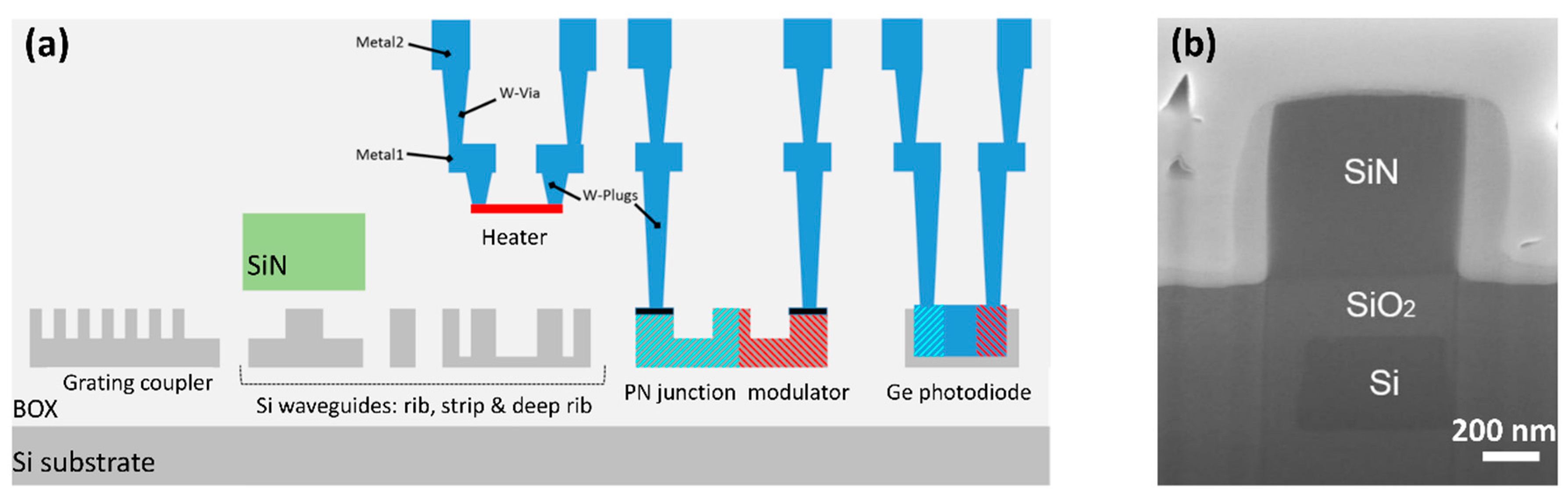
2. Fabrication Process and Waveguide Performances

2.1. Fabrication Processes

Over the last few years, our silicon photonics platform has become increasingly mature. High-performance optical components have been developed and repeatedly tested to build a complete device library [2] with reproducible performance. This Si platform is the starting point for the integration of the SiN layer. The process starts with 200 mm Silicon-on-Insulator (SOI) substrates with 300-nm-thick Si and buried oxide (BOX) thickness of 2 µm. The Si process flow is designed to support various sets of devices using a multilevel etch defining silicon thicknesses of 50, 150 and 300 nm. A Deep Ultra Violet 193 nm lithography is used to pattern all three silicon etching levels providing an overlay control below 50 nm and definition of various shapes (isolated and arrayed lines and trenches) with critical dimensions as low as 120 nm (see Figure 1a). A Si3N4 hard mask is used for the first Si level, ensuring low waveguide roughness leading to low optical propagation losses in silicon waveguides.
To integrate an additional layer on top of the patterned Si, one needs to start with a flat oxide surface. Oxide encapsulation of patterned Si structures is therefore followed by Chemical Mechanical Polishing (CMP) to planarize the top oxide down to the Si3N4 hard mask. The presence of dummy structures allows a high enough Si density for clear end point detection. This process is followed by another SiO2 deposition. With a median value of 207 nm of SiO2 on top of Si and a standard deviation of 4 nm over the 200 mm wafers, this process provides a flat surface with a very good uniformity of the interlayer thickness, which is important for hybrid devices such as Si-SiN grating couplers or Si-SiN transitions. Integrating a new material while staying compatible with a CMOS process imposes several challenges. In particular, a low thermal budget is necessary to prevent degradation of other components, in particular, active devices with doped regions. In addition, the new material should not induce further mechanical deflection of the wafer to maintain a low bow, compatible with the 200 mm facilities. Depending on the targeted applications, we developed two different silicon nitride integration processes, taking into account the aforementioned constraints: a low stress, low deposition temperature non-stoichiometric SiN in the O-band and a nearly stoichiometric Si3N4 material with a low quantity of residual N–H bonds for lower absorption in the C-band. The former is used when preservation of the doping profile of active devices (p-n Si modulator and Ge photodiode) is the prime concern and is preferred for applications such as optical transceivers for datacom in the O-band where the material absorption is very low. The latter is used for applications in the C-band, where N–H bonds must be eliminated to minimize optical absorption.
• SiNx for optical transceiver for Datacom in the O-band
To preserve the doping of implanted active devices, we developed a plasma-enhanced chemical vapor deposition (PECVD), non-stoichiometric, low-stress SiNx deposition process at 300 °C. The SiN film thickness is 600 nm (see Figure 1b), and its refractive index, measured by ellipsometry, is nSiNx = 1.88 at 1.31 µm. This rather low value indicates the deposited film is not stoichiometric with a rather high fraction of nitrogen.
• Si3N4 for wideband comb generation
To control strain and to prevent cracks from appearing, the silicon nitride layer is deposited via low-pressure chemical vapor deposition (LPCVD) in two steps of 370-nm-thick layers each [32]. The deposition is carried out with a tailored ultra-low deposition rate (<2 nm/min) to produce a very high-quality film. Furthermore, between the two deposition stages, the wafer is rotated by 45° in order to distribute the uniaxial strain along the overall film thickness, thus avoiding film cracks upon subsequent subtractive patterning. Each deposition run is carried out at 780 °C with post-deposition cooling to around 630 °C for 20 min. The resulting film is close to stoichiometry, and its optical index is nSi3N4 = 2 (more details will be given in the nonlinear Section 4).
• SiN for near infrared LIDAR
For LIDAR applications in the near infrared, both types of SiN can be used indifferently; however, stoichiometric Si3N4 shows slightly lower losses at a wavelength of ~900 nm. For this application we therefore chose a 300 nm thick Si3N4. Finally, a 10/100 nm Ti/TiN metal layer separated by a certain distance from the SiN layer was incorporated. This layer can be used to form resistive wires (heater in Figure 1a), allowing for phase shifts in the SiN waveguides using the thermo-optic effect. Electrical contact to the heater was achieved using vias and AlCu contact pads.
All types of silicon nitride waveguides are patterned using 248 nm Deep Ultra Violet (DUV) lithography and CF4-CH2F2-O2 chemistry-based reactive-ion etching. The produced structures range from 200 nm tips, spaces and lines to hundreds of micrometers. The selective etching provides a low edge roughness and a vertical sidewall. Figure 1b shows a FIB cross-section of the final Si-SiN stack with a 200 nm SiO2 interlayer thickness. SiN structures are encapsulated by 1 µm SiO2 before optical characterization.

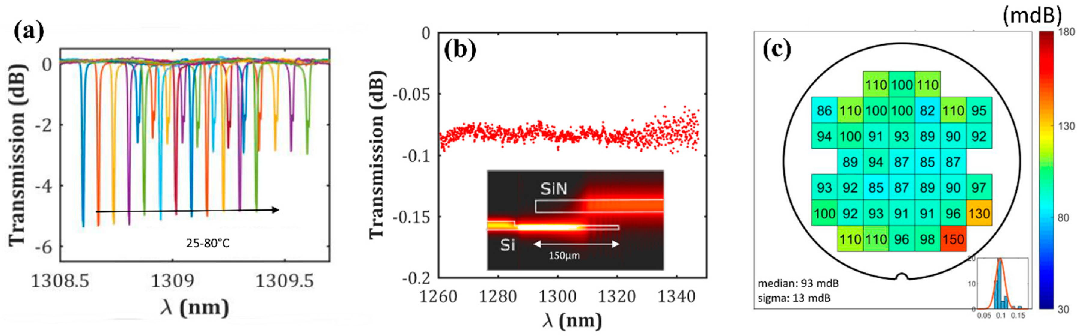
2.2. SiN Waveguide Optical Characterization

We characterized the fabricated SiN structures in terms of propagation losses, bend losses and thermal properties. In addition, we obtained state-of-the-art performances for Si-SiN interlayer transition, making it possible to fully exploit the potential of the multilayer Si-SiN platform. SiN waveguides and structures are characterized on a semi-automatic 12-inch probe station at the wafer level with a tunable laser source (Tunics T100S, Yenista, Lannion, France) and its complementary photodetector (CT400, Yenista, Lannion, France) with pm resolution. A fiber-to-fiber setup is used for propagation loss measurements. Unless mentioned otherwise, devices are characterized through surface grating couplers with a scattering angle of 11.5° (8° in the SiO2 cladding), which is compatible with packaging standards.
• SiN waveguide propagation and bend losses
The propagation and bend losses of Si and SiN single-mode waveguides are summarized in Table 1. Propagation losses are extracted from the transmission of 20-, 40- and 60-mm-long spiraled waveguides, de-embedded from the grating coupler transmission, on up to 45 dies for each wafer. Notably, thanks to a measurement conducted at the 200mm wafer level, we are able to extract statistical data which is reported in Table 1. In Si, both strip and rib losses (3.6 and 1.5 dB/cm respectively) are consistent with the previously reported silicon waveguides characteristics [2], and we can conclude that adding the SiN layer does not affect the performance of the Si waveguides. As expected, propagation losses are much lower in SiN thanks to a lower sensitivity to waveguide roughness, itself resulting from a lower optical index contrast with the SiO2 cladding compared to Si. We obtain 0.8 dB/cm in the O-band for the PECVD SiNx, 1.5 dB/cm in the C-band for 750 nm thick LPCVD Si3N4 and 1 (1.5) dB/cm at 940 nm for 300-nm-thick Si3N4 (SiNx respectively). The higher propagation loss measured in the C-band for LPCVD Si3N4 is probably due to remaining N–H bonds causing absorption, despite a deposition process tailored to minimize the amount of residual hydrogen atoms.
Due to a low mode confinement (itself due to the low optical index), SiN bend waveguides require a higher bend radius compared to Si to minimize the bend losses. For the 600-nm-thick PECVD SiNx (the lowest optical index), we measure 0.06, 0.03 and 0.015 dB/90° bend for radii of 20, 30 and 40 µm, respectively. In the 300-nm-thick LPCVD Si3N4, thanks to a higher optical index, losses are below 0.01 dB for a 15 µm radius bend. As a comparison, in Si, we measure 90° bend losses below 0.03 dB for both 30 µm radius bend rib waveguide and 9 µm radius bend strip waveguide.
• PECVD SiN thermo-optic coefficient
The thermo-optic coefficient of SiNx is estimated by measuring the wavelength resonance thermal shift of a ring resonator. The resonance spectra acquired at temperatures from 25 °C to 80 °C of a 30 µm radius SiNx ring coupled to an adjacent bus waveguide are shown in Figure 2a. The resonance spectral shift is 14 pm/K, which translates into a thermo-optic coefficient of 1.7 × 10⁻⁵ K−1. This value is indeed more than one order of magnitude lower than for silicon in telecommunication bands, which confirms the relevance of SiN for applications where thermal stability is essential, as for the (de-)multiplexer.
• Si-SiN interlayer transition with PECVD SiN
To fully exploit a multi-layer Si-SiN platform, there is a need for a compact, efficient and broadband interlayer transition between Si and SiN [20,35,36,37]. These requirements are well satisfied using adiabatic taper interlayer transitions. The principle of the interlayer transition is to reduce the dimension of the high index waveguide to lower its effective index below the effective index of the low index waveguide. Due to the large index difference between Si and SiN, index matching requires narrowing the Si waveguide down to the smallest width allowed by the design rules. In addition, our multi-level Si platform also allows narrowing the Si waveguide height to a thickness of 150 nm. Therefore, we designed a Si-SiN transition based on inverse tapers of Si and SiN using a tip width at the minimum dimension permitted by the design rule i.e., 120 nm in Si and 200 nm in SiN, with a Si height of 150 nm and a length of 150 µm. A side view of the optical power profile after beam propagation method (BPM) simulation is shown in the inset of Figure 2b.
From up to 90 cascaded Si-SiN transitions, we extract the single transition spectrum shown in Figure 2b. It shows a particularly flat spectrum, with a 0.09 dB insertion loss over the 1260–1350 nm range. Figure 2c, the wafer map of this measurement indicates very uniform performances of the transition with a median insertion loss of 0.093 dB and a 3 sigma of 0.04 dB. We believe this good uniformity is due to the well-controlled SiO2 interlayer thickness. Included in this value is the insertion loss (measured at 0.02 dB) of the transition from 300-nm-thick to 150-nm-thick Si waveguides, which is 30 µm long. The total insertion loss of the transition is comparable to the normal propagation losses of an equivalent length of waveguide.

3. SiN for Coarse Wavelength Division Multiplexing (CWDM) Optical Transceivers in the O-Band

CWDM is a standard providing a channel spacing of 20 nm that is large enough to tolerate the possible wavelength deviation of the lasers. It is, therefore, an attractive solution to increase the data rate of optical transceivers while using uncooled laser, which limits the power-consumption of the transceiver. However, for a 4-channel CWDM transceiver, the optical bandwidth of the circuit reaches 80 nm, making the waveguide-to-fiber coupling difficult with a Si grating. Thanks to its low optical index, an SiN-based grating presents a larger bandwidth, which is helpful for CWDM circuit testing [38]. In this section, we present a CWDM SiN multiplexer with a low thermal sensitivity and a SiN-based grating coupler for broadband fiber coupling.

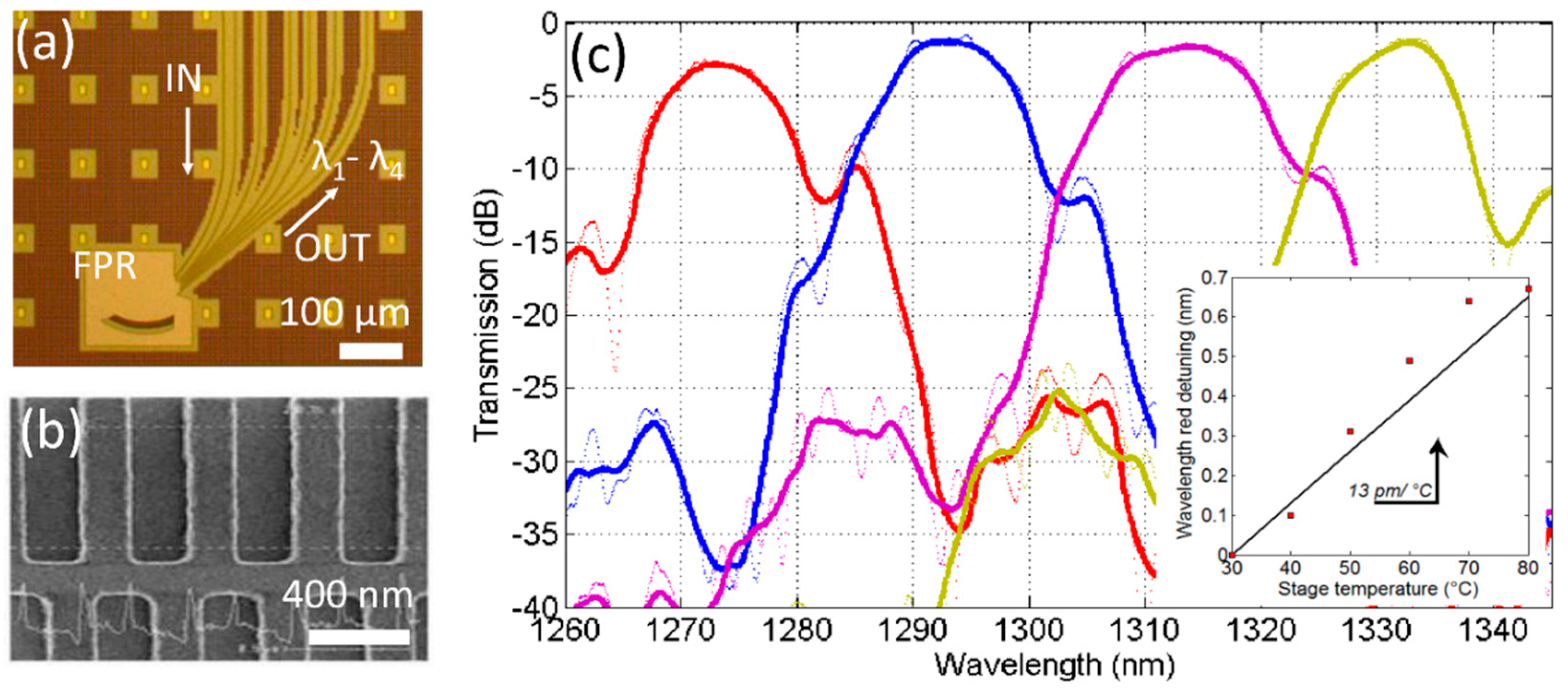
3.1. CWDM SiN Echelle Grating Multiplexer

Echelle gratings (EG) are diffraction grating spectrometers whose principle is based upon phase matching the light reflected from neighboring facets. Using a slab waveguide as a free propagation region (FPR), we describe a simple grating on a classic Rowland mounting using the following equation [39]:
d ( sin θ i + sin θ m ) = m λ n e f f ( λ )
where θi (70°) and θm (88°) are the angles of incidence and diffraction of the mth (3rd) diffraction order, λ is the wavelength in free space, d (1.76 µm) is the spacing of the grating teeth, and neff (1.748) is the effective index of the slab mode at 1310 nm, while the Rowland mounting radius is 55 µm. In particular, the input access waveguide to the FPR was tapered from 700 nm up to 2.4 µm in order to minimize the scattering losses at the entrance of the slab region due to the modal propagation mismatch between the effective indices of the slab and the rib. Concerning the output, an array of multimode waveguides (MMWs) 2.2 µm in width ensures wide channel bandwidth and low insertion losses, while maintaining high interchannel isolation. In addition, the grating teeth were blazed, chirped and oriented to focus the light into the selected diffraction order, and dimensioned according to the proximity of the neighboring teeth in order to reduce cross-shadowing, thus enhancing performance.
Optical and scanning electron microscope (SEM) images of the EGs (de-)multiplexers are illustrated in Figure 3a,b, respectively. A close to 90% reflectivity of the EG facets is ensured through the use of 1st-order DBRs with a 50% fill factor and 422-nm periodicity (Figure 3b). For this device, a slightly different fabrication process was used to show the full potential of SiN Echelle Multiplexer: Dose-optimized 8-inch VISTEC variable-shape e-beam lithography was used for the SiN patterning. A 300-nm-thick PECVD-grown SiO2 layer over the SiN layer was used as a hard mask for protecting the waveguides from ion bombardment during encapsulation, as well as to ensure optimum pattern transfer from the e-beam resist to the nitride layer.
The results are shown in Figure 3c. The measurements reveal insertion losses averaging 1.5 dB across the four transmission channels, an average interchannel isolation above 30 dB (when determined at the center of the transmission channel), and a precise channel spacing of nearly 20 nm. A −1 dB channel bandwidth varying between 7 and 9 nm and a channel-to-channel non-uniformity of 1.4 dB were found. As well as that, phase errors arising from local facet imperfections or non-verticality both have an impact on the defocusing of the image spot at the output, impinging slightly on insertion losses.
The thermal chromatic dispersion (i.e., the temperature-related wavelength shift) of the device itself when operating at increasing temperature is also important, as it impacts the flexibility of the device when operating in radically different environments, especially at the receiver side of the optical link. Recently, state-of-the-art SiN Mach-Zehnder multiplexers have been realized, with a reported thermal chromatic dispersion of 18.5 pm/°C [17]. Similar measurements were carried out on the SiN EGs presented in this paper, indicating an even lower thermal detuning coefficient, measured at below 13 pm/°C, as shown in the inset of Figure 3c. This is possible thanks to the EG operating over a slab FPR instead of rib/strip waveguides. In fact, the effective index variation of a slab waveguide is noticeably lower compared to those of strip or rib waveguides, making SiN EGs an attractive solution on the path toward quasi-athermal behavior.

3.2. SiN-Si Hybrid Grating Fiber Coupler

The transmission characteristics of single polarization grating couplers (SPGC) are often summarized in terms of the minimum insertion loss and the −1dB (or −3 dB) bandwidth (BW). While these figures of merit provide a useful comparison between different designs, for SPGCs destined for use in WDM applications, it may be more practical to consider the range of insertion loss values directly over the entire utilized spectrum. Typical values for the insertion loss/−1 dB BW of a standard silicon O-band SPGC are 2–4 dB/20–30 nm. Such grating couplers, centered at 1310 nm, have insertion losses of at least 10 dB at the extremes of the CWDM band, ruling out their use in CWDM systems and even rendering reliable wafer-scale characterization of CWDM devices difficult. While it may be difficult to envisage the deployment of grating coupler-based fiber couplers in CWDM systems in preference to non-diffractive coupling methods (particularly in the receiver circuit, due to complications relating to the unknown incoming polarization state in the fiber), large-bandwidth SPGCs would be an invaluable tool for the development of the CWDM device library.
It can be generally said that, for a given fiber type, a wider transmission band will result from a reduction in the effective index of the grating. While using materials with lower optical indices (such as SiN) to make fiber grating couplers tends to lead to wider transmission spectra, these gains are often associated with increased insertion losses. The inclusion of the SiN layer in this process allowed us to compare Si, SiN and hybrid SiN/Si SPGCs for their use in CWDM applications and device testing. The standard Si SPGC is a partially etched (300/150 nm nominal Si thicknesses), apodised design. The SiN grating design is based on fully etched SiN lines and trenches, optimized for a peak transmission at 1310 nm. The BOX thickness is 2 µm, but with the SiN being 200 nm above the Si layer, the total substrate-SiN distance is 2.5 µm. Figure 4a,b shows a hybrid SiN/Si design as introduced by Sacher et al. [38]. The SiN waveguide is connected to a primary, fully etched grating, beneath which is a secondary Si grating. The secondary Si grating, while having the same period, may be displaced with respect to the primary SiN grating (denoted as ΔxSi in Figure 4a, which allows a lithographic control over the grating directionality. This is not possible with a conventional single-layer grating, where the directionality is fixed by the thickness of the etched and unetched layer thicknesses. As was also demonstrated in [38], allowing the fiber angle to be a free parameter allows further optimization of the grating directionality for a particular BOX thickness. In this study, however, the fiber angle was fixed to the typical standard value of 8° (in the SiO2 cladding) to allow compatibility with standard test and packaging procedures.
Figure 4c shows the results of 2D-FDTD simulations of the transmission spectra of the Si-only (black line) SPGC (into an optimally placed SMF28 fiber). This grating has a simulated group index (ng) value that varies from 3.0 to 2.88, a −1 dB BW of 30 nm and an insertion loss of 1.6 dB to 13 dB over the CWDM band. The SiN-only grating coupler (blue line) has a ng value of 1.56, a −1 dB bandwidth of 54 nm, and an insertion loss of 6.8 dB to 10.0 dB over the CWDM band. Varying the various free parameters of the SiN/Si hybrid SPGC in order to minimize the insertion loss of the CWDM band led to a simulated -1 dB bandwidth of 64 nm (the ng value of 1.58 is very similar to the SiN-only grating) and insertion losses of −3.0 dB to 5.5 dB (dashed green line). This represents a significant improvement to both the Si-only and SiN-only grating couplers for CWDM applications. The solid green line in Figure 4c shows the simulated transmission spectrum of the best-performing fabricated design, as described below. The various design parameters and simulated transmission characteristics of each SPGC type are summarized in Table 2.
For a more accurate measurement of grating coupler transmission, a fiber array with height control is used to couple the incident light in a reproducible way across the 200 mm wafer. Figure 4d shows the measured coupling efficiency for the apodised Si design (black line), the uniform SiN design (blue line) and the best-performing SiSiN design (green line). The measurements show good correspondence between the simulated and measured values, the insertion loss values are typically several tenths of dBs higher than the simulated values, which may be accounted for by taking into account reflections caused at the cladding/air and air/fiber interfaces in the measurement. Among the various SiN/Si design variants tested, the design with the lowest insertion losses over the CWDM band had slightly different geometrical parameters compared to the best-performing simulated design (See Table 2). This is presumably due to inaccuracies in the SiN/Si relative mask alignment and slight differences in the simulated and processed grating element morphology. A wafer-scale measurement over 43 dies gives a median minimum insertion loss of −3 dB with a 3 sigma of 0.46 dB and a median maximum insertion loss over the entire CWDM band of −5.8 dB with a 3 sigma of 0.77 dB. These results confirm the suitability of this type of SPGC as a reliable wafer-level characterization tool for CWDM components.

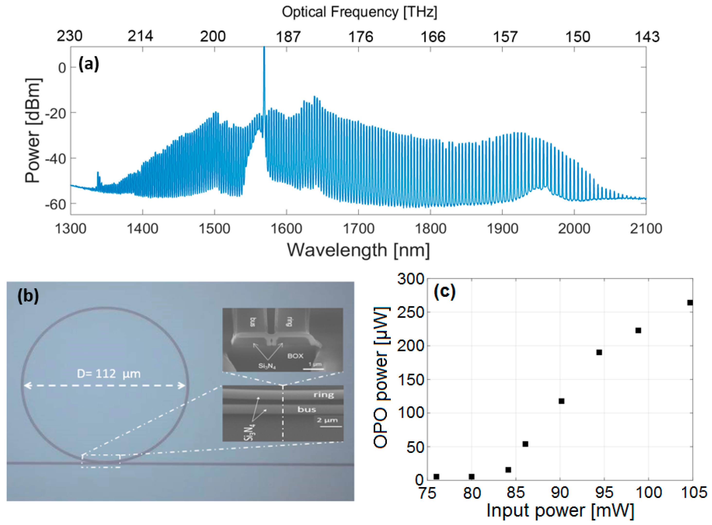
4. Optical Frequency Comb Generation in Annealing- and Crack-Free Si3N4

Kerr optical frequency combs (OFCs) constitute a paradigm shift in the development of high-capacity data transmission, high-precision metrology, frequency synthesis, and integrated spectroscopy [14]. Since 2010, silicon-nitride-on-insulator (SiNOI) has been seen as an attractive chip-based platform for the generation of wideband frequency combs pumped at telecom wavelengths, because of its relatively high nonlinearity (×6 larger than that of highly nonlinear Hydex glass [13]), as well as the absence of two-photon absorption and free carrier generation, which plague crystalline silicon. In this context, the monolithic integration of Kerr-based frequency combs with Si photonics and CMOS circuits paves the way for on-chip high-capacity transmitters that would benefit from the maturity and low cost of CMOS manufacturing and scalability.
The realization of relatively thick (>7–800 nm) stoichiometric Si3N4 films, as required by microring frequency combs, which imply both a tight confinement of light and anomalous group velocity dispersion (GVD), remains challenging. In particular, all prior works have systematically made use of N2-atmosphere long high-temperature annealing of the deposited silicon nitride film at >1200 °C for at least 3 h [12,40,41,42]. This rather extreme annealing step has been accounted for by the need to densify the silicon nitride film by driving out excess hydrogen and to break N-H bonds, so as to get closer to a stoichiometric Si3N4 film, reducing the material absorption loss in the C-band. Such annealing induces stress, eventually leading to crack formation during device processing unless sophisticated pre-patterning strategies are adopted prior to the film deposition [40,41]. Now, from the perspective of silicon optoelectronics-nonlinear optics co-integration, such extreme annealing cycles would severely degrade the front-end-of-the-line (FEOL) silicon optoelectronic circuits underneath. Specifically, doped components and circuits would be unacceptably affected by the undesirable dopant diffusion in junction-based Si modulators and by the hetero-interface degradation of Ge-on-Si photodetectors. As an alternative, in 2013, optical parametric oscillation was demonstrated by using the proprietary composition of Hydex microresonators [13]. As previously stated, the nonlinear parameter γ of Hydex is 6 times lower than silicon nitride. Consequently, generating frequency combs in such material requires more power, increasing the risk of waveguide fusing, and device failure.
In early 2018, we reported a new method that avoids thermal annealing for growing relatively thick (740 nm) crack-free Si3N4-based straight nanowaveguides with good linear and nonlinear properties measured by self-phase modulation [33].
Here, we report a comb generated by a micro-resonator fabricated by an intrinsically CMOS-compatible annealing-free silicon nitride, following a tailored deposition method which minimizes the hydrogen content instead of hour-long 1200 °C post-annealing. Our annealing-free and crack-free fabrication process provides our devices with the right specifications (i.e., micro-ring group velocity dispersion and characteristics) to underpin Kerr frequency combs, thus representing a significant step toward the full compatibility of Si3N4-based Kerr comb sources with the thermal budgets of Si photonics processing.
To control the strain and to prevent cracks from appearing, the silicon nitride layer is deposited on a (non-patterned) substrate via low-pressure chemical vapor deposition (LPCVD) in two steps of 370-nm-thick layers each. The deposition is performed with a tailored ultra-low deposition rate (~2 nm/min) to yield a very high quality film [33]. Under such low deposition rates, the thermal activation energy enables silicon and nitrogen to be disposed at the silicon nitride film surface via atomic surface migration phenomena, while compelling hydrogen to escape the film. Furthermore, between the two deposition stages, the wafer is rotated by 45° in order to distribute the uniaxial strain along the overall film thickness, thus avoiding film cracks upon subsequent subtractive patterning. Each deposition run is carried out at 780 °C with post-deposition cooling to around 630 °C for 20 min. Controlled ramp-ups and -downs from/to 780 °C at 10 °C/minute to/from 630 °C are used prior to each deposition, which is carried out under a 112 mTorr pressure using NH3 (200 sccm) and SiH2Cl2 (80 sccm) as precursor gases. By measuring the wafer bow, before and after removing the silicon nitride from the wafer back side, the material morphological characterization revealed a tensile strain around +1200 MPa, highlighting the as-deposited stoichiometry of the material and minimization of residual hydrogen content [41].
The optical spectrum out of an annealing-free silicon-nitride-on-insulator micro-ring with a 56 µm radius is shown in Figure 5a. An optical picture of the ring is shown in Figure 5b. The cross-section dimensions (1.5 µm-wide × 740 nm-thick) of the ring waveguide ensure that GVD is anomalous at the 1569 nm pump wavelength. The loaded quality factor of the microring—which is separated by a 350 nm gap from the bus waveguide—exceeds 580,000. A relatively smooth native line spacing (~406 GHz) frequency comb spanning about 800 nm between 1300 nm and 2100 nm is obtained for ~1 W continuous-wave power (Pin) coupled in the bus waveguide (i.e., a value comparable to that required for similar rings in high-temperature annealed Si3N4 [43]. The Optical parametric Oscillator (OPO) threshold power was measured to be around 83 mW (see Figure 5c).
In conclusion, these results [32] show that it is possible to generate a wideband comb at telecom wavelengths using annealing-free silicon nitride nonlinear circuits featuring a full FEOL process compatibility with Si photonics. Via such demonstration, we claim the first-time realization of annealing-free silicon nitride frequency comb microresonators, following a tailored deposition method, minimizing the hydrogen content. Our annealing-free and crack-free fabrication process provides our devices with the right specification (microring group velocity dispersion and characteristics) to underpin Kerr frequency combs, thus representing a significant step toward the full compatibility of Si3N4-based Kerr-comb sources monolithic integration with standard CMOS and Si photonics processing.

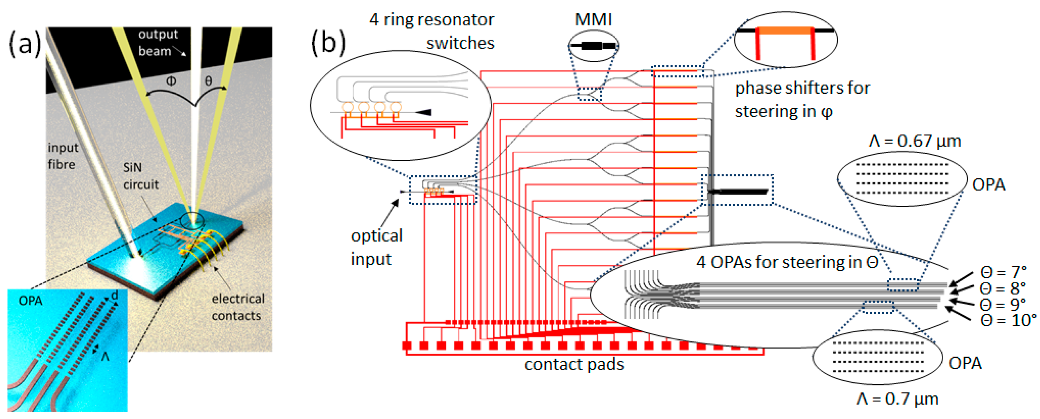
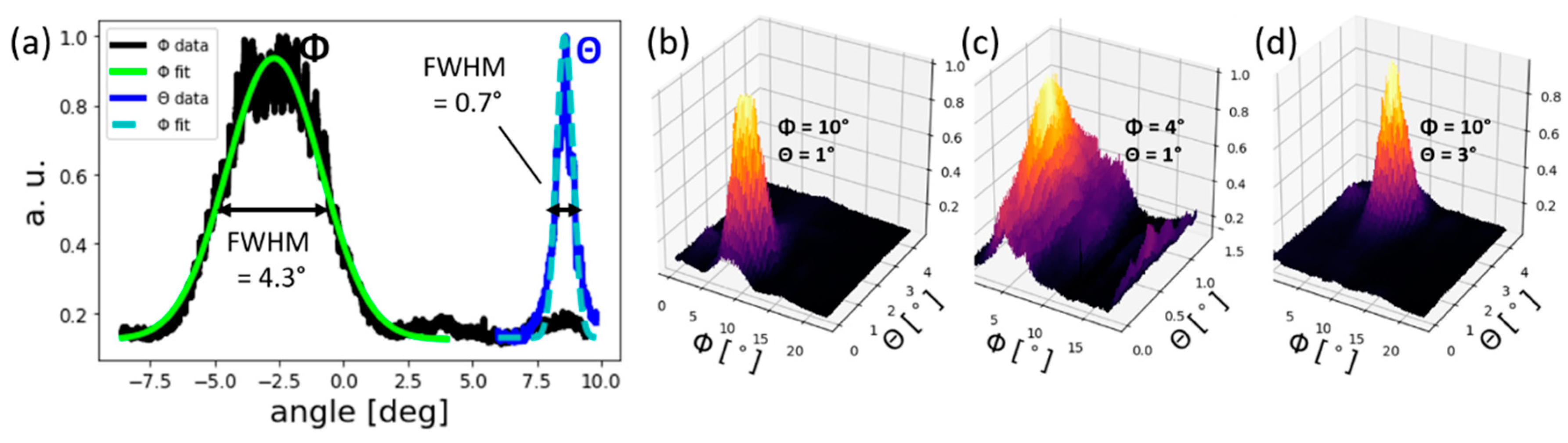
5. SiN for Near Infrared LIDAR

Over the last decade, optical phased arrays (OPAs) have attracted significant attention due to their potential use in a broad range of advanced technological applications, including light detection and ranging (LIDAR), free space communication, and holographic displays [8]. This interest arises from the advantage that OPAs enable non-mechanical, arbitrary beam shaping and steering. Furthermore, it has been shown that OPAs can be implemented using integrated photonics, creating a path for miniaturized low-cost systems [9,44,45]. OPA integration has been explored on various photonic platforms, of which silicon photonics is particularly attractive due to its CMOS compatibility and high refractive index contrast [46]. Advanced OPA circuits have been demonstrated at telecommunications wavelengths using silicon, such as a fully integrated device for two-dimensional beam scanning [10], ultra-low divergence beams [11,34], and coherent LIDAR circuits [47,48]. However, the use of silicon provides some limitations in terms of wavelength transparency and maximum optical power. Here, the use of (SiN) presents a host of interesting possibilities, as outlined in the following.
Compared to Si, which absorbs light at photon energies greater than its bandgap (~1100 nm) the transparency window of SiN is much larger and is suited for applications at wavelengths down to at least 500 nm. Furthermore, weak nonlinear losses allow SiN circuits to operate at higher optical powers than Si, which is important for time-of-flight LIDAR. SiN has recently been demonstrated for OPA integration [34,49,50].
To allow the construction of proof-of-concept OPA circuits, we designed and characterized (typical measured insertion losses at λ = 905 nm shown in brackets) a new device library. Key components include fiber grating couplers (−4.9 dB), single-mode straight and bent waveguides (−1.0 dB/cm, minimum bend radius ~15 µm), 1 × 2 multimode interference splitters (0.12 dB), heater-based phase modulators (87 mW/π), ring resonators, and output grating couplers.
To demonstrate the use of this platform for LIDAR applications, we used these building blocks to design an optical circuit comprising four small OPA circuits linked to a single optical input via a switching network, with which we demonstrated rudimentary two-dimensional beam steering at a fixed wavelength of λ = 905 nm (see Figure 6) [51].
To demonstrate the functionality of the OPA circuit, we put in place a set-up that allows wafer-level beam calibration of the far field emission. A fiber couples 905 nm light to the circuit via the input fiber grating coupler, a multi-channel electrical probe allows the application of up to 25 individual drive voltages to the circuit and the output light is detected in the far field by a full frame CMOS camera placed above the OPA output. Custom driving electronics work in conjunction with the camera via a hill-climbing optimization algorithm to form a beam at the desired output angle.
The normalized cross-sections in ϕ and θ of the main lobe of the optimized beam are shown in Figure 7a in black and blue, respectively. A Gaussian curve was fitted to the data in order to obtain the full width at half maximum (FWHM). The measured FWHM are 4.3° and 0.7° in ϕ and θ. Both values are in in good agreement with the expected beam FWHM in ϕ of 4.3° (calculated from the OPA geometry) and 0.6° in θ (from FDTD simulations of the output grating coupler).
The OPA output beam was steered in ϕ over a range of 17.6°, limited by the appearance of higher-order diffraction lobes, and over a range of 3° in θ, by routing to various OPAs using the ring-based routing sub-circuit. A selection of beam steering results are shown in Figure 7b–d, where the normalized intensity plots of the beam recorded by the camera can be seen for angles of ϕ/θ = 10°/1°, ϕ/θ = 4°/1° and ϕ/θ = 10°/3°, respectively.
These results demonstrate the possibilities offered by the SiN-based integrated photonics platform for free-space applications at near infrared wavelengths. In the case of integrated beam steering circuits for LIDAR, further development of individual components and circuit architecture will allow the evolution of the current proof-of-concept circuits into circuits that satisfy the scanning range, resolution and power consumption requirements of real-world systems. In addition, although these circuits use only the SiN layer for waveguiding due to the optical transparency at the operating wavelength, the proximity of an underlying silicon layer provides several possibilities, such as for monitoring photodiodes and reflecting layers for reducing substrate losses at the output grating couplers.
Furthermore, expansion of the current near-infrared device library and farfield characterization system may allow the possibility of using SiN-based integrated photonics for other types of free-space imaging systems such as facial recognition.

6. Conclusions

We have presented the development and several applications of a flexible multilayer Si-SiN CMOS-compatible photonics platform. Regarding datacom applications, we have shown how SiN allows the realization of robust and quasi-temperature insensitive (de-)multiplexers for CWDM optical transceivers, as well as for broadband fiber grating couplers. Another promising application of SiN in telecom and datacom is for frequency comb generation, which we have demonstrated in a non-annealed Si3N4 micro-resonator. Finally, by exploiting the wide transparency range of SiN, we presented a functioning integrated OPA for 2D beam steering, operating in the near infrared, at 905 nm. In the context of silicon photonics platform maturation, these results show the versatility, as well as the relative simplicity, of SiN guiding layer integration, thus opening the way to a wide range of large-scale and low-cost applications.

Author Contributions

Conceptualization, C.S., D.F., S.M. and S.O.; Investigation, Q.W., H.E.D., N.T., C.S., D.F., S.G., M.C., S.K., K.H. and A.K.; Project administration, X.L., L.K.O., W.R., B.S. and S.O.; Supervision, C.S., D.F., S.M., C.M., X.L., M.P., K.Y., L.K.O., W.R. and S.O.; Writing—original draft, Q.W., C.S. and D.F.; Writing—review & editing, Q.W., D.F. and S.O.

Funding

This work has received funding from the European Union Horizon H2020 Program (H2020-ICT27-2015) under grant agreement COSMICC n°688516, the DOPT 2020 internal funding program (CEA-LETI), the Danish Research Council SPOC (DNRF-123) center of excellence silicon photonics for communications (SPOC) (DTU), the ERC H2020 GRAPHICS (648546), the Institut Universitaire de France (INL), and the French Direction Générale des Entreprises (DGE) via the DEMO3S project.

Acknowledgments

The authors acknowledge A. Myko, P. Grosse and O. Lemonnier for valuable help in the measurement setup mounting, and R. Crochemore, C. Socquet-Clerc and D. Despois for their help in the fabrication process.

Conflicts of Interest

The authors declare no conflict of interest.

References

  1. Boeuf, F.; Cremer, S.; Temporiti, E.; Fere, M.; Shaw, M.; Baudot, C.; Vulliet, N.; Pinguet, T.; Mekis, A.; Masini, G.; et al. Silicon Photonics R&D and Manufacturing on 300-mm Wafer Platform. J. Lightw. Technol. 2016, 34, 286–295. [Google Scholar] [CrossRef]
  2. Szelag, B.; Blampey, B.; Ferrotti, T.; Reboud, V.; Hassan, K.; Malhouitre, S.; Grand, G.; Fowler, D.; Brision, S.; Bria, T.; et al. Multiple Wavelength Silicon Photonic 200 mm R + D Platform for 25Gb/s and above Applications. In Proceedings of the Silicon Photonics and Photonic Integrated Circuits V, Brussels, Belgium, 3–7 April 2016; Volume 9891, p. 98911C. [Google Scholar]
  3. Horikawa, T.; Shimura, D.; Okayama, H.; Jeong, S.-H.; Takahashi, H.; Ushida, J.; Sobu, Y.; Shiina, A.; Tokushima, M.; Kinoshita, K.; et al. A 300-mm Silicon Photonics Platform for Large-Scale Device Integration. IEEE J. Sel. Top. Quantum Electron. 2018, 24, 1–15. [Google Scholar] [CrossRef]
  4. Wang, J.; Long, Y. On-chip silicon photonic signaling and processing: A review. Sci. Bull. 2018, 63, 1267–1310. [Google Scholar] [CrossRef]
  5. Silverstone, J.W.; Bonneau, D.; O’Brien, J.L.; Thompson, M.G. Silicon Quantum Photonics. IEEE J. Sel. Top. Quantum Electron. 2016, 22, 390–402. [Google Scholar] [CrossRef]
  6. Politi, A.; Cryan, M.J.; Rarity, J.G.; Yu, S.; O’Brien, J.L. Silica-on-Silicon Waveguide Quantum Circuits. Science 2008, 320, 646–649. [Google Scholar] [CrossRef] [Green Version]
  7. Qiang, X.; Zhou, X.; Wang, J.; Wilkes, C.M.; Loke, T.; O’Gara, S.; Kling, L.; Marshall, G.D.; Santagati, R.; Ralph, T.C.; et al. Large-scale silicon quantum photonics implementing arbitrary two-qubit processing. Nat. Photonics 2018, 12, 534–539. [Google Scholar] [CrossRef]
  8. Heck, M.J.R. Highly integrated optical phased arrays: Photonic integrated circuits for optical beam shaping and beam steering. Nanophotonics 2017, 6, 93–107. [Google Scholar] [CrossRef]
  9. Van Acoleyen, K.; Bogaerts, W.; Jágerská, J.; Le Thomas, N.; Houdré, R.; Baets, R. Off-chip beam steering with a one-dimensional optical phased array on silicon-on-insulator. Opt. Lett. 2009, 34, 1477–1479. [Google Scholar] [CrossRef] [PubMed]
  10. Hulme, J.C.; Doylend, J.K.; Heck, M.J.R.; Peters, J.D.; Davenport, M.L.; Bovington, J.T.; Coldren, L.A.; Bowers, J.E. Fully integrated hybrid silicon two dimensional beam scanner. Opt. Express 2015, 23, 5861–5874. [Google Scholar] [CrossRef]
  11. Chung, S.; Abediasl, H.; Hashemi, H. A Monolithically Integrated Large-Scale Optical Phased Array in Silicon-on-Insulator CMOS. IEEE J. Solid State Circuits 2018, 53, 275–296. [Google Scholar] [CrossRef]
  12. Levy, J.S.; Gondarenko, A.; Foster, M.A.; Turner-Foster, A.C.; Gaeta, A.L.; Lipson, M. CMOS-compatible multiple-wavelength oscillator for on-chip optical interconnects. Nat. Photonics 2010, 4, 37–40. [Google Scholar] [CrossRef]
  13. Moss, D.J.; Morandotti, R.; Gaeta, A.L.; Lipson, M. New CMOS-compatible platforms based on silicon nitride and Hydex for nonlinear optics. Nat. Photonics 2013, 7, 597–607. [Google Scholar] [CrossRef] [Green Version]
  14. Marin-Palomo, P.; Kemal, J.N.; Karpov, M.; Kordts, A.; Pfeifle, J.; Pfeiffer, M.H.P.; Trocha, P.; Wolf, S.; Brasch, V.; Anderson, M.H.; et al. Microresonator-based solitons for massively parallel coherent optical communications. Nature 2017, 546, 274–279. [Google Scholar] [CrossRef] [Green Version]
  15. Duan, G.-H.; Jany, C.; Le Liepvre, A.; Accard, A.; Lamponi, M.; Make, D.; Kaspar, P.; Levaufre, G.; Girard, N.; Lelarge, F.; et al. Hybrid III–V on Silicon Lasers for Photonic Integrated Circuits on Silicon. IEEE J. Sel. Top. Quantum Electron. 2014, 20, 158–170. [Google Scholar] [CrossRef]
  16. Durel, J.; Ferrotti, T.; Chantre, A.; Cremer, S.; Harduin, J.; Bernabé, S.; Kopp, C.; Boeuf, F.; Ben Bakir, B.; Broquin, J.-E. Realization of Back-Side Heterogeneous Hybrid III-V/Si DBR Lasers for Silicon Photonics. In Proceedings of the Integrated Optics: Devices, Materials and technologies XX, San Francisco, CA, USA, 13–18 February 2016; Volume 9750, p. 97500O. [Google Scholar]
  17. Szelag, B.; Hassan, K.; Adelmini, L.; Ghegin, E.; Rodriguez, P.; Bensalem, S.; Nemouchi, F.; Bria, T.; Brihoum, M.; Brianceau, P.; et al. Hybrid III-V/Si DFB laser integration on a 220 mm fully CMOS-compatible silicon photonics platform. In Proceedings of the 2017 IEEE International Electron Devices Meeting (IEDM), San Francisco, CA, USA, 2–6 December 2017. [Google Scholar]
  18. Virot, L.; Benedikovic, D.; Szelag, B.; Alonso-Ramos, C.; Karakus, B.; Hartmann, J.-M.; Le Roux, X.; Crozat, P.; Cassan, E.; Marris-Morini, D.; et al. Integrated waveguide PIN photodiodes exploiting lateral Si/Ge/Si heterojunction. Opt. Express 2017, 25, 19487–19496. [Google Scholar] [CrossRef]
  19. Ferrotti, T.; Blampey, B.; Jany, C.; Duprez, H.; Chantre, A.; Boeuf, F.; Seassal, C.; Ben Bakir, B. Co-integrated 13µm hybrid III-V/silicon tunable laser and silicon Mach-Zehnder modulator operating at 25 Gb/s. Opt. Express 2016, 24, 30379–30401. [Google Scholar] [CrossRef]
  20. Sacher, W.D.; Huang, Y.; Lo, G.-Q.; Poon, J.K.S. Multilayer Silicon Nitride-on-Silicon Integrated Photonic Platforms and Devices. J. Lightw. Technol. 2015, 33, 901–910. [Google Scholar] [CrossRef]
  21. Rahim, A.; Ryckeboer, E.; Subramanian, A.Z.; Clemmen, S.; Kuyken, B.; Dhakal, A.; Raza, A.; Hermans, A.; Muneeb, M.; Dhoore, S.; et al. Expanding the Silicon Photonics Portfolio With Silicon Nitride Photonic Integrated Circuits. J. Lightw. Technol. 2017, 35, 639–649. [Google Scholar] [CrossRef] [Green Version]
  22. Zhang, Z.; Yako, M.; Ju, K.; Kawai, N.; Chaisakul, P.; Tsuchizawa, T.; Hikita, M.; Yamada, K.; Ishikawa, Y.; Wada, K. A new material platform of Si photonics for implementing architecture of dense wavelength division multiplexing on Si bulk wafer. Sci. Technol. Adv. Mater. 2017, 18, 283–293. [Google Scholar] [CrossRef]
  23. Wilmart, Q.; Fowler, D.; Sciancalepore, C.; Hassan, K.; Plantier, S.; Adelmini, L.; Garcia, S.; Robin-Brosse, D.; Malhouitre, S.; Olivier, S. A hybrid SOI/SiN photonic platform for high-speed and temperature-insensitive CWDM optical transceivers. In Proceedings of the Silicon Photonics XIII, San Francisco, CA, USA, 27 January–1 February 2018; Volume 10537, p. 1053709. [Google Scholar]
  24. Boeuf, F.; Baudot, C.; Le Maitre, P.; Vulliet, N.; Planchot, J.; Babaud, L.; Carpentier, J.-F.; Messaoudene, S.; Khedim, M.; Orlandi, P.; et al. Evaluation of Advanced Process Integration Options for Next Generation of Si-Photonics Platform. In Proceedings of the International Conference on Solid State Devices and Materials, Tokyo, Japan, 9–13 September 2018. [Google Scholar]
  25. Baets, R.; Subramanian, A.Z.; Clemmen, S.; Kuyken, B.; Bienstman, P.; Le Thomas, N.; Roelkens, G.; Van Thourhout, D.; Helin, P.; Severi, S. Silicon Photonics: Silicon nitride versus silicon-on-insulator. In Proceedings of the Optical Fiber Communication Conference, Anaheim, CA, USA, 20–22 March 2016. [Google Scholar]
  26. Arbabi, A.; Goddard, L.L. Measurements of the refractive indices and thermo-optic coefficients of Si3N4 and SiO_x using microring resonances. Opt. Lett. 2013, 38, 3878–3881. [Google Scholar] [CrossRef]
  27. Iadanza, S.; Bakoz, A.P.; Singaravelu, P.K.J.; Panettieri, D.; Schulz, S.A.; Devarapu, G.C.R.; Guerber, S.; Baudot, C.; Boeuf, F.; Hegarty, S.; et al. Thermally stable hybrid cavity laser based on silicon nitride gratings. Appl. Opt. 2018, 57, E218–E223. [Google Scholar] [CrossRef] [PubMed]
  28. Gao, G.; Chen, D.; Tao, S.; Zhang, Y.; Zhu, S.; Xiao, X.; Xia, J. Silicon nitride O-band (de)multiplexers with low thermal sensitivity. Opt. Express 2017, 25, 12260–12267. [Google Scholar] [CrossRef] [PubMed]
  29. Bucio, T.D.; Khokhar, A.Z.; Mashanovich, G.Z.; Gardes, F.Y. Athermal silicon nitride angled MMI wavelength division (de)multiplexers for the near-infrared. Opt. Express 2017, 25, 27310–27320. [Google Scholar] [CrossRef] [PubMed]
  30. Pommarede, X.; Hassan, K.; Billondeau, P.; Hugues, V.; Grosse, P.; Charbonnier, B.; Duan, G.-H. 16x100 GHz Echelle Grating-Based Wavelength Multiplexer on Silicon-on-Insulator Platform. IEEE Photonics Technol. Lett. 2017, 29, 493–495. [Google Scholar] [CrossRef]
  31. Dong, P. Silicon Photonic Integrated Circuits for Wavelength-Division Multiplexing Applications. IEEE J. Sel. Top. Quantum Electron. 2016, 22, 370–378. [Google Scholar] [CrossRef]
  32. El Dirani, H.; Kamel, A.; Casale, M.; Kerdiles, S.; Monat, C.; Letartre, X.; Pu, M.; Oxenløwe, L.K.; Yvind, K.; Sciancalepore, C. Annealing-free Si3N4 frequency combs for monolithic integration with Si photonics. Appl. Phys. Lett. 2018, 113. [Google Scholar] [CrossRef]
  33. El Dirani, H.; Casale, M.; Kerdiles, S.; Socquet-Clerc, C.; Letartre, X.; Monat, C.; Sciancalepore, C. Crack-Free Silicon-Nitride-on-Insulator Nonlinear Circuits for Continuum Generation in the C-Band. IEEE Photonics Technol. Lett. 2018, 30, 355–358. [Google Scholar] [CrossRef]
  34. Poulton, C.V.; Byrd, M.J.; Raval, M.; Su, Z.; Li, N.; Timurdogan, E.; Coolbaugh, D.; Vermeulen, D.; Watts, M.R. Large-scale silicon nitride nanophotonic phased arrays at infrared and visible wavelengths. Opt. Lett. 2017, 42, 21–24. [Google Scholar] [CrossRef]
  35. Bauters, J.F. Ultra-Low Loss Waveguides with Application to Photonic Integrated Circuits; University of California: Santa Barbara, CA, USA, 2013. [Google Scholar]
  36. Huang, Y.; Song, J.; Luo, X.; Liow, T.-Y.; Lo, G.-Q. CMOS compatible monolithic multi-layer Si3N4-on-SOI platform for low-loss high performance silicon photonics dense integration. Opt. Express 2014, 22, 21859–21865. [Google Scholar] [CrossRef] [PubMed]
  37. Hosseinnia, A.H.; Atabaki, A.H.; Eftekhar, A.A.; Adibi, A. High-quality silicon on silicon nitride integrated optical platform with an octave-spanning adiabatic interlayer coupler. Opt. Express 2015, 23, 30297–30307. [Google Scholar] [CrossRef] [PubMed]
  38. Sacher, W.D.; Huang, Y.; Ding, L.; Taylor, B.J.F.; Jayatilleka, H.; Lo, G.-Q.; Poon, J.K.S. Wide bandwidth and high coupling efficiency Si3N4-on-SOI dual-level grating coupler. Opt. Express 2014, 22, 10938–10947. [Google Scholar] [CrossRef] [PubMed]
  39. Sciancalepore, C.; Lycett, R.J.; Dallery, J.A.; Pauliac, S.; Hassan, K.; Harduin, J.; Duprez, H.; Weidenmueller, U.; Gallagher, D.F.G.; Menezo, S.; et al. Low-Crosstalk Fabrication-Insensitive Echelle Grating Demultiplexers on Silicon-on-Insulator. IEEE Photonics Technol. Lett. 2015, 27, 494–497. [Google Scholar] [CrossRef]
  40. Luke, K.; Dutt, A.; Poitras, C.B.; Lipson, M. Overcoming Si3N4 film stress limitations for high quality factor ring resonators. Opt. Express 2013, 21, 22829–22833. [Google Scholar] [CrossRef] [PubMed]
  41. Pfeiffer, M.H.P.; Kordts, A.; Brasch, V.; Zervas, M.; Geiselmann, M.; Jost, J.D.; Kippenberg, T.J. Photonic Damascene process for integrated high-Q microresonator based nonlinear photonics. Optica 2016, 3, 20–25. [Google Scholar] [CrossRef]
  42. Kim, S.; Han, K.; Wang, C.; Jaramillo-Villegas, J.A.; Xue, X.; Bao, C.; Xuan, Y.; Leaird, D.E.; Weiner, A.M.; Qi, M. Dispersion engineering and frequency comb generation in thin silicon nitride concentric microresonators. Nat. Commun. 2017, 8, 372. [Google Scholar] [CrossRef] [PubMed]
  43. Herr, T.; Hartinger, K.; Riemensberger, J.; Wang, C.Y.; Gavartin, E.; Holzwarth, R.; Gorodetsky, M.L.; Kippenberg, T.J. Universal formation dynamics and noise of Kerr-frequency combs in microresonators. Nat. Photonics 2012, 6, 480–487. [Google Scholar] [CrossRef] [Green Version]
  44. Vasey, F.; Reinhart, F.K.; Houdré, R.; Stauffer, J.M. Spatial optical beam steering with an AlGaAs integrated phased array. Appl. Opt. 1993, 32, 3220–3232. [Google Scholar] [CrossRef]
  45. Guo, W.; Binetti, P.R.A.; Althouse, C.; Masanovic, M.L.; Ambrosius, H.P.M.M.; Johansson, L.A.; Coldren, L.A. Two-Dimensional Optical Beam Steering with InP-Based Photonic Integrated Circuits. IEEE J. Sel. Top. Quantum Electron. 2013, 19. [Google Scholar] [CrossRef]
  46. Jalali, B.; Fathpour, S. Silicon Photonics. J. Lightw. Technol. 2006, 24, 4600–4615. [Google Scholar] [CrossRef]
  47. Poulton, C.V.; Yaacobi, A.; Cole, D.B.; Byrd, M.J.; Raval, M.; Vermeulen, D.; Watts, M.R. Coherent solid-state LIDAR with silicon photonic optical phased arrays. Opt. Lett. 2017, 42, 4091–4094. [Google Scholar] [CrossRef]
  48. Martin, A.; Dodane, D.; Leviandier, L.; Dolfi, D.; Naughton, A.; O’Brien, P.; Spuessens, T.; Baets, R.; Lepage, G.; Verheyen, P.; et al. Photonic Integrated Circuit-Based FMCW Coherent LiDAR. J. Lightw. Technol. 2018, 36, 4640–4645. [Google Scholar] [CrossRef]
  49. Sabouri, S.; Jamshidi, K. Design Considerations of Silicon Nitride Optical Phased Array for Visible Light Communications. IEEE J. Sel. Top. Quantum Electron. 2018, 24. [Google Scholar] [CrossRef]
  50. Zadka, M.; Chang, Y.-C.; Mohanty, A.; Phare, C.T.; Roberts, S.P.; Lipson, M. On-chip platform for a phased array with minimal beam divergence and wide field-of-view. Opt. Express 2018, 26, 2528–2534. [Google Scholar] [CrossRef] [PubMed]
  51. Tyler, N.; Fowler, D.; Malhouitre, S.; Garcia, S.; Grosse, P.; Rabaud, W.; Szelag, B. SiN integrated optical phased arrays for 2-dimensional beam steering at a single near-infrared wavelength. Under review. Opt. Express. 2018, unpublished. [Google Scholar]
Figure 1. (a) Cross-section of the full Si-SiN platform based on SOI 300nm (gray waveguides) and SiN (green waveguide), together with metallic heaters, PN modulator, Ge photodiode and metallic interconnection. The BOX is 2 µm. (b) SEM cross-section view obtained by FIB cut of Si and SiN waveguides. Si is 300 nm thick, SiN is 600 nm thick. The interlayer SiO2 thickness is 200 nm.
Applsci 09 00255 g001
Figure 2. (a) SiN ring resonance shift against T. Each color represents a measurement at a different temperature, from 25 °C to 80 °C. The resonance shift with temperature allows to extract the SiN thermo-optic coefficient α = 1.7 × 10⁻⁵ K−1. (b) Measured spectrum of the Si-SiN transition insertion loss. Inset: side view of the transition with the optical mode from a BPM simulation. (c) Wafer mapping of the transition insertion loss (in mdB). Inset: histogram of the wafer level insertion loss. The median value is 0.09 dB and the standard deviation is 0.01 dB.
Applsci 09 00255 g002
Figure 3. Optical (a) and scanning electron microscope (SEM) (b) images of the CWDM echelle grating (de)-multiplexer realized on 200-mm SiNOI platform. Close-up SEM pictures of the DBR-assisted facets used to improve the grating reflectivity. (c) Transmission spectrum of the 20-nm-spaced 4-channels echelle grating de-multiplexer across the O-band. Raw data (dashed line) and fitted plot (solid lines). (inset) Wavelength red detuning between 30 °C and 80 °C reveals a thermal dispersion coefficient of 13 pm/°C.
Applsci 09 00255 g003
Figure 4. (a) Schematic side view of the SiN/Si grating; (b) SEM image of the hybrid SiN-Si grating coupler; (c) Simulated insertion loss of the apodised Si design (black line), the uniform SiN design (blue line), the best-performing simulated SiSiN design (dashed green line), and the best-performing fabricated SiSiN design (solid green line). (d) Same as (c), but for the measured designs.
Applsci 09 00255 g004
Figure 5. Comb generation using annealing-free silicon nitride on insulator. (a) An 800-nm-spanning comb generation using a 56-µm-radius Si3N4 microresonator for Pin ~ 1 W. (b) Optical microscope and (insets) scanning electron microscope images of the ring and coupling region. (c) Plot of short-wavelength OPO power with input power in the bus waveguide.
Applsci 09 00255 g005
Figure 6. (a) Artistic illustration of an integrated OPA. The output beam (depicted in white) can be steered in two dimensions (represented in yellow). (b) Schematic image of the proposed two-dimensional beam steering circuit. A switching network allows access to four different OPAs, each with a distinct emission angle in θ. Phase shifters allow the introduction of a phase difference between the OPA channels for beam steering in Φ.
Applsci 09 00255 g006
Figure 7. (a) Cross-sections in ϕ and θ of the main lobe to determine the FWHM. (bd) Examples of output beam intensity profiles showing beam steering in two dimensions.
Applsci 09 00255 g007
Table 1. Si and SiN waveguide properties and propagation losses.
WaveguideSi RibSi StripSiN PECVD 1310 nmSi3N4 LPCVD 1550 nmSiN PECVD 940 nmSi3N4 LPCVD 940 nm
dimension w × h (µm)0.4 × 0.30.35 × 0.30.7 × 0.60.75 × 0.750.6 × 0.30.6 × 0.3
Propagation Loss (dB/cm)1.53.60.81.51.51.0
3 sigma (dB/cm)0.450.90.3--0.4
Table 2. Summary of grating parameters and simulated and measured insertion loss (IL) and bandwidth (BW).
Grating TypePeriod (nm)ΔxSi (nm)Unetched/Etched Thickness (nm)2D-FDTD CWDM IL (nm)2D-FDTD 1 dB BW (nm)Measured CWDM IL (dB)Measured 1 dB BW (nm)
Si468–488-300/1501.6–15301.9–13.026
SiN965-6006.8–10.0548.0–13.045
Si/SiN a9502006003.0–5.564--
Si/SiN b975150600/502.7–6.9502.9–5.248
a Simulated and b measured designs with lowest losses over the CWDM band.

