Diffusion and Dopant Activation in Germanium: Insights from Recent Experimental and Theoretical Results


Abstract
:
1. Introduction
2. Self-Diffusion
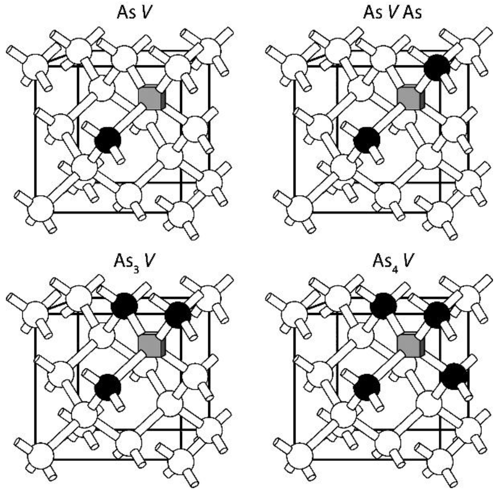
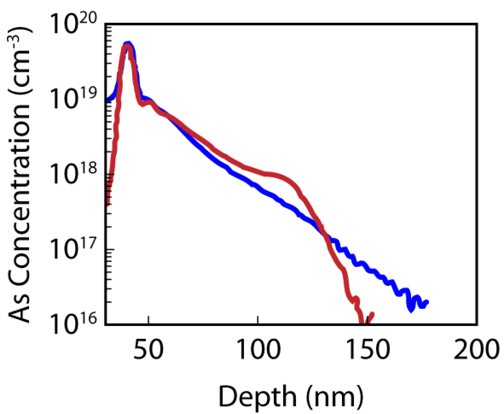
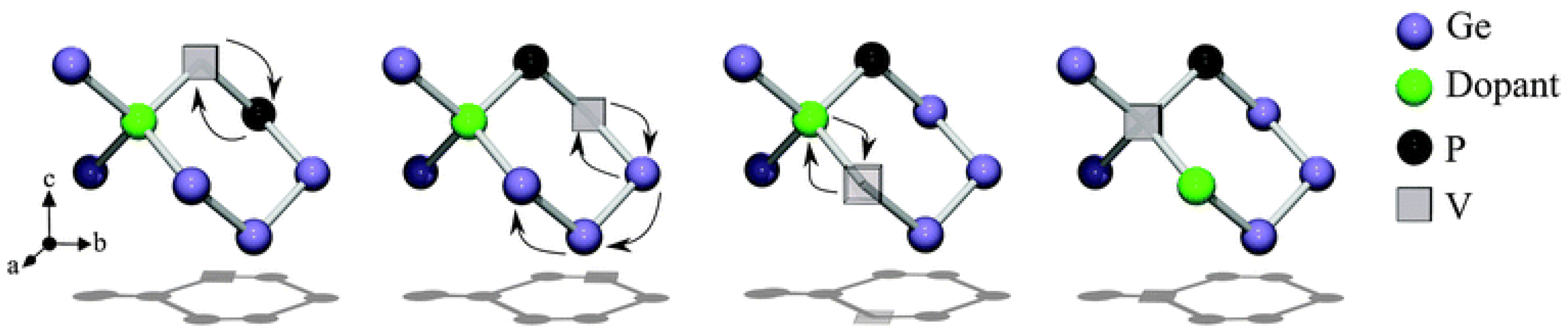
3. n-Type Dopants
4. p-Type Dopants
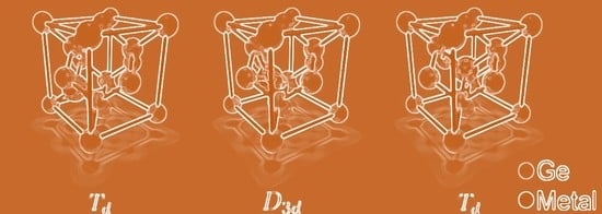
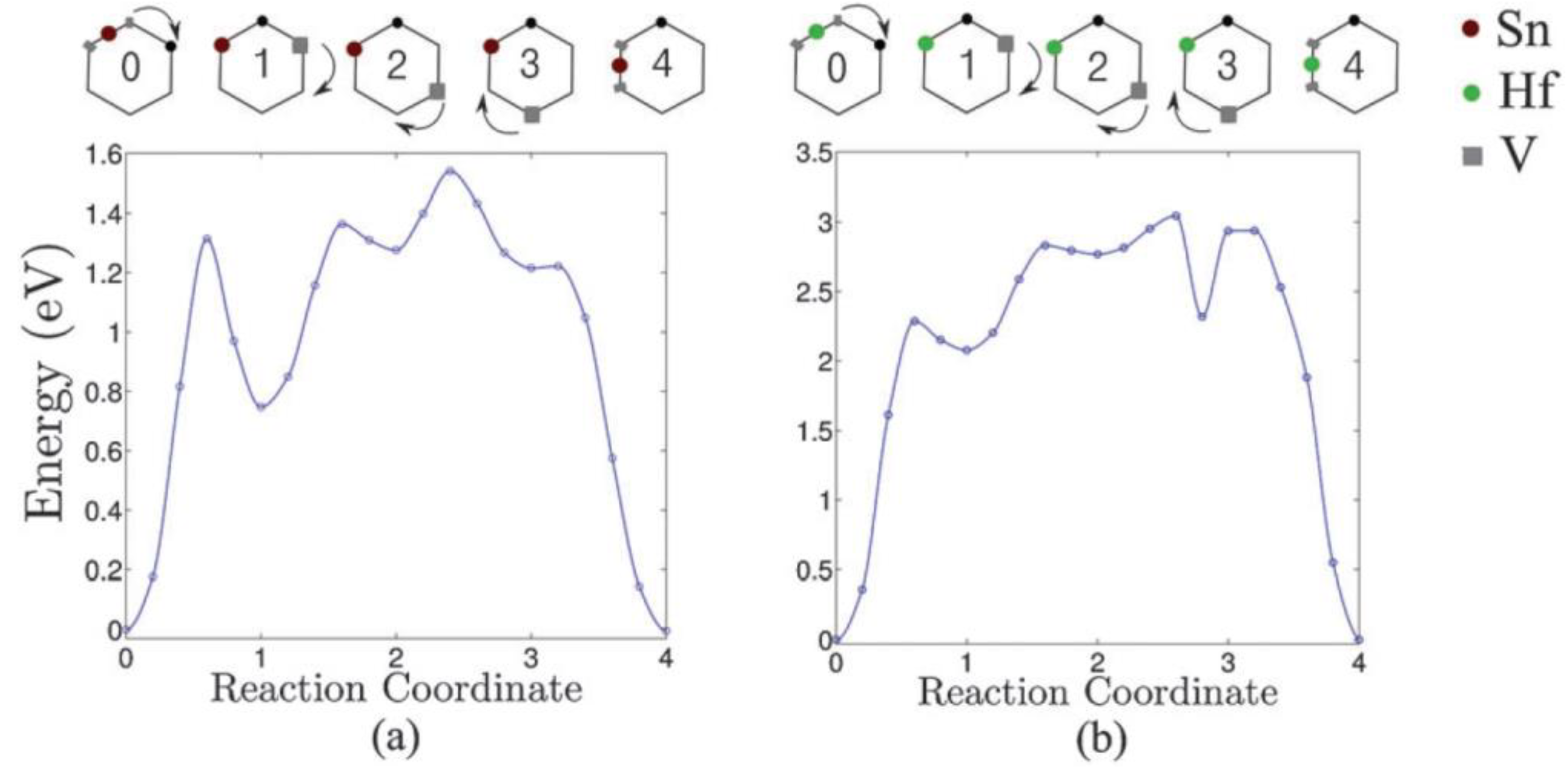
5. Isovalent Dopants
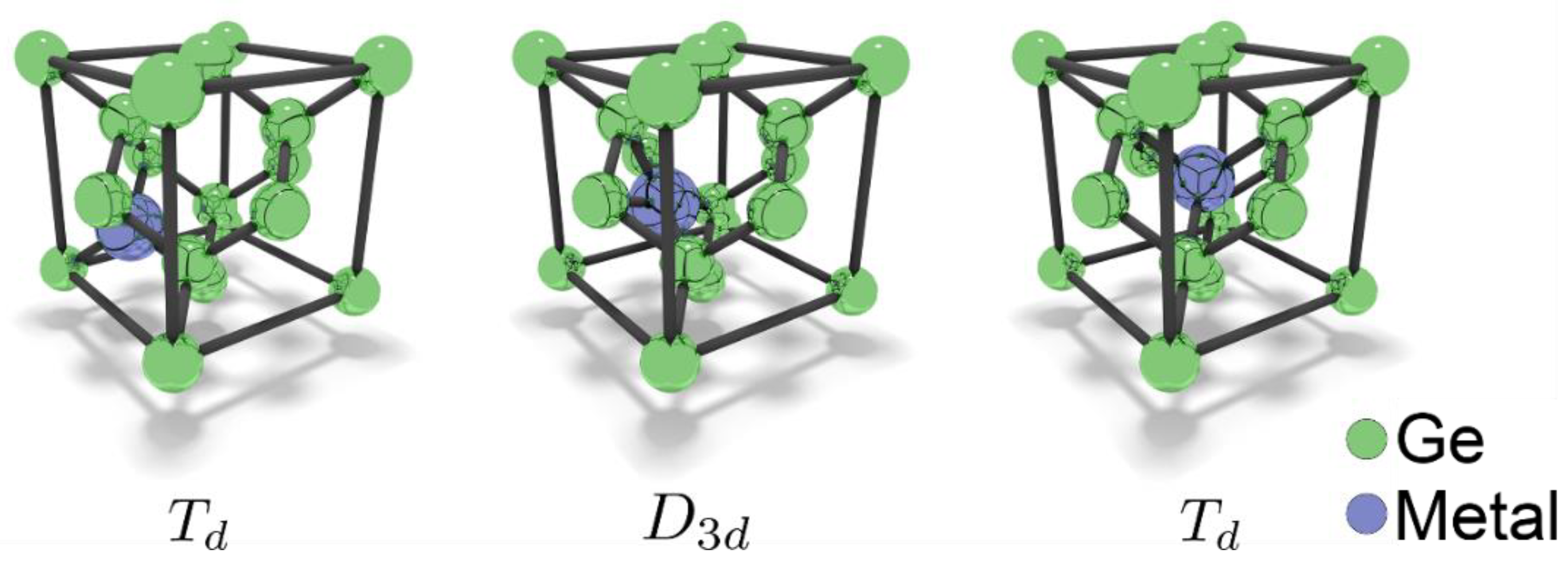
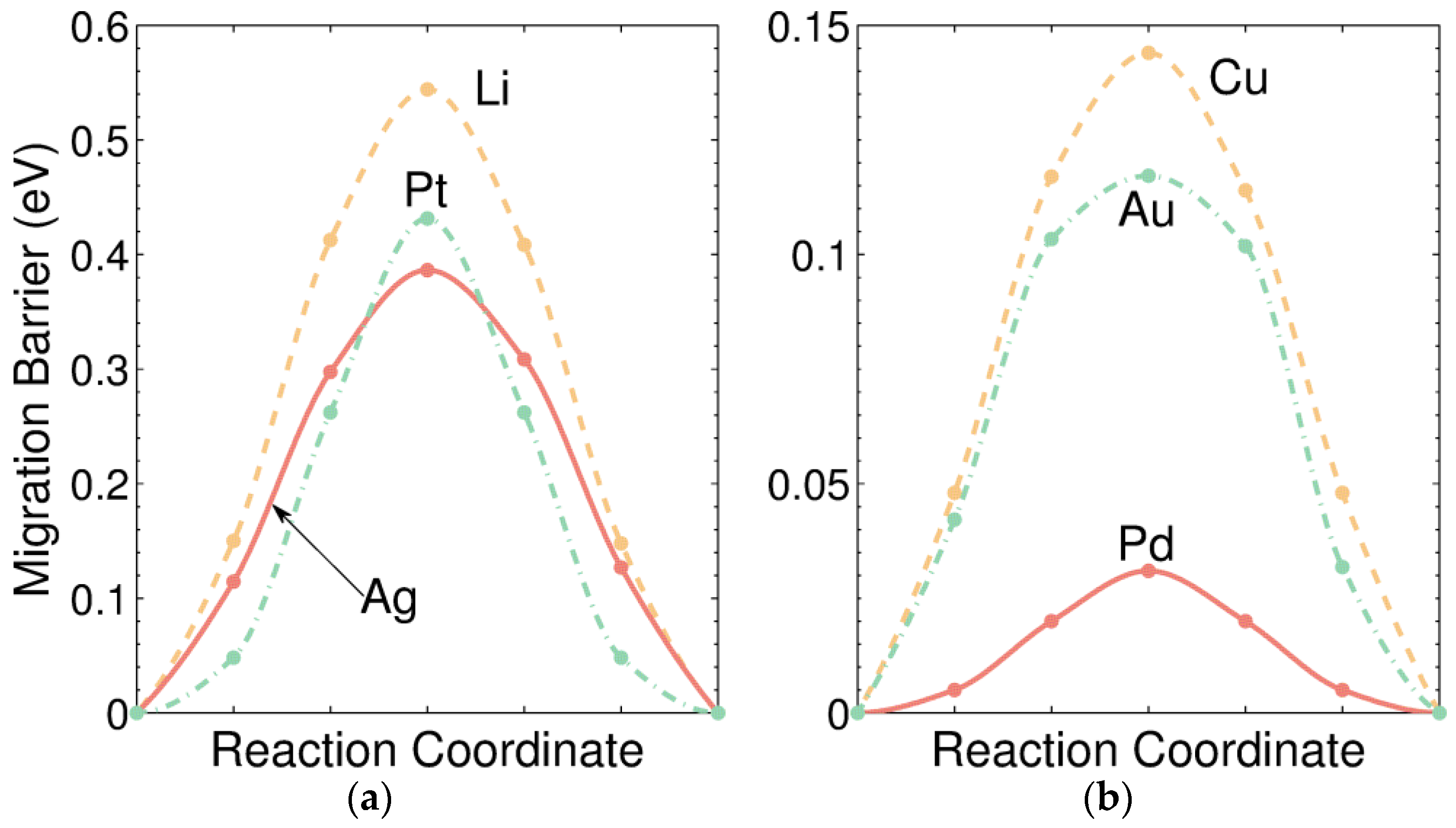
6. Metal Atom Diffusion
7. Oxygen Diffusion
8. Summary
Author Contributions
Funding
Conflicts of Interest
References
- Claeys, C.; Simoen, E. Germanium-Based Technologies: From Materials to Devices; Elsevier: Amsterdam, The Netherlands, 2007. [Google Scholar]
- Impellizzeri, G.; Boninelli, S.; Priolo, F.; Napolitani, E.; Spinella, C.; Chroneos, A.; Bracht, H. Fluorine effect on As diffusion in Ge. J. Appl. Phys. 2011, 109, 113527. [Google Scholar] [CrossRef]
- Stolwijk, N.A.; Bracht, H. Diffusion in Silicon, Germanium and their Alloys; Landolt-Börnstein New Series, Vol. III/33; Subvolume A Springer: New York, NY, USA, 1998. [Google Scholar]
- Chroneos, A.; Grimes, R.W.; Uberuaga, B.P.; Brotzmann, S.; Bracht, H. Vacancy-arsenic clusters in germanium. Appl. Phys. Lett. 2007, 91, 192106. [Google Scholar] [CrossRef]
- Bracht, H.; Brotzmann, S. Atomic transport in germanium and the mechanism of arsenic diffusion. Mater. Sci. Semicond. Proc. 2006, 9, 471–476. [Google Scholar] [CrossRef]
- Pinto, H.M.; Coutinho, J.; Torres, V.J.B.; Öberg, S.; Briddon, P.R. Formation energy and migration barrier of a Ge vacancy from ab initio studies. Mater. Sci. Semicond. Proc. 2006, 9, 498–502. [Google Scholar] [CrossRef]
- Tsouroutas, P.; Tsoukalas, D.; Florakis, A.; Zergioti, I.; Serafetinides, A.A.; Cherkashin, N.N.; Marty, B.; Claverie, A. Laser annealing for n+/p junction formation in germanium. Mater. Sci. Semicond. Proc. 2006, 9, 644–649. [Google Scholar] [CrossRef]
- Chroneos, A.; Skarlatos, D.; Tsamis, C.; Christofi, A.; McPhail, D.S.; Hung, R. Implantation an diffusion of phosphorous in germanium. Mater. Sci. Semicond. Proc. 2006, 9, 640–643. [Google Scholar] [CrossRef]
- Chroneos, A. Isovalent impurity-vacancy complexes in germanium. Phys. Status Solidi B 2007, 244, 3206–3210. [Google Scholar] [CrossRef]
- Janke, C.; Jones, R.; Coutinho, J.; Öberg, S.; Briddon, P.R. Ab initio investigation of phosphorus diffusion paths in germanium. Phys. Rev. B 2008, 77, 195210. [Google Scholar] [CrossRef]
- Chroneos, A.; Bracht, H.; Grimes, R.W.; Uberuaga, B.P. Phosphorous clustering in germanium-rich silicon germanium. Mater. Sci. Eng. B 2008, 154–155, 72–75. [Google Scholar] [CrossRef]
- Silvestri, H.H.; Bracht, H.; Hansen, J.L.; Larsen, A.N.; Haller, E.E. Diffusion of silicon in crystalline germanium. Semicond. Sci. Technol. 2006, 21, 758–762. [Google Scholar] [CrossRef] [Green Version]
- Naganawa, M.; Shimizu, Y.; Uematsu, M.; Itoh, K.M.; Sawano, K.; Shiraki, Y.; Haller, E.E. Charge states of vacancies in germanium investigated by simultaneous observation of germanium self-diffusion and arsenic diffusion. Appl. Phys. Lett. 2008, 93, 191905. [Google Scholar] [CrossRef] [Green Version]
- Schneider, S.; Bracht, H.; Petersen, M.C.; Lundsgaard Hansen, J.; Nylandsted Larsen, A. Proton irradiation of germanium isotope multilayer structures at elevated temperatures. J. Appl. Phys. 2008, 103, 033517. [Google Scholar] [CrossRef]
- Haller, E.E. Germanium: From its discovery to SiGe devices. Mater. Sci. Semicond. Proc. 2006, 9, 408–422. [Google Scholar] [CrossRef] [Green Version]
- Tahini, H.; Chroneos, A.; Grimes, R.W.; Schwingenschlögl, U.; Dimoulas, A. Strain induced changes to the electronic structure of germanium. J. Phys. Condens. Matter 2012, 24, 195802. [Google Scholar] [CrossRef] [PubMed]
- Bruno, E.; Mirabella, S.; Scapellato, G.; Impellizzeri, G.; Terrasi, A.; Priolo, F.; Napolitani, E.; De Salvador, D.; Mastramatteo, M.; Carnera, A. Mechanism of B diffusion in crystalline Ge under proton irradiation. Phys. Rev. B 2009, 80, 033204. [Google Scholar] [CrossRef]
- Kube, R.; Bracht, H.; Chroneos, A.; Posselt, M.; Schmidt, B. Intrinsic and extrinsic diffusion of indium in germanium. J. Appl. Phys. 2009, 106, 063534. [Google Scholar] [CrossRef] [Green Version]
- Decoster, S.; De Vries, B.; Wahl, U.; Correia, J.G.; Vantomme, A. Lattice location study of implanted In in Ge. J. Appl. Phys. 2009, 105, 083522. [Google Scholar] [CrossRef]
- Tahini, H.; Chroneos, A.; Grimes, R.W.; Schwingenschlögl, U. Diffusion of tin in germanium: A GGA+U approach. Appl. Phys. Lett. 2011, 99, 162103. [Google Scholar] [CrossRef]
- Hüger, E.; Tietze, U.; Lott, D.; Bracht, H.; Bougeard, D.; Haller, E.E.; Schmidt, H. Self-diffusion in germanium isotope multilayers at low temperatures. Appl. Phys. Lett. 2008, 93, 162104. [Google Scholar] [CrossRef] [Green Version]
- Chroneos, A.; Bracht, H.; Jiang, C.; Uberuaga, B.P.; Grimes, R.W. Nonlinear stability of E centers in Si1−xGex: Electronic structure calculations. Phys. Rev. B 2008, 78, 195201. [Google Scholar] [CrossRef]
- Chroneos, A. Effect of germanium substrate loss and nitrogen on dopant diffusion in germanium. J. Appl. Phys. 2009, 105, 056101. [Google Scholar] [CrossRef]
- Chroneos, A. Dopant-vacancy cluster formation in germanium. J. Appl. Phys. 2010, 107, 076102. [Google Scholar] [CrossRef] [Green Version]
- Pulikkotil, J.J.; Chroneos, A.; Schwingenschlögl, U. Structure of Sn1−xGex random alloys as obtained from the coherent potential approximation. J. Appl. Phys. 2011, 110, 036105. [Google Scholar] [CrossRef]
- Chroneos, A.; Londos, C.A. Interaction of A-centers with isovalent impurities in silicon. J. Appl. Phys. 2010, 107, 093518. [Google Scholar] [CrossRef] [Green Version]
- Wang, W.; Chroneos, A.; Londos, C.A.; Sgourou, E.N.; Schwingenschlögl, U. A-centers in silicon studied with hybrid density functional theory. Appl. Phys. Lett. 2013, 103, 052101. [Google Scholar] [CrossRef] [Green Version]
- Werner, M.; Mehrer, H.; Hochheimer, H.D. Effect of hydrostatic pressure, temperature, and doping on self-diffusion in germanium. Phys. Rev. B 1985, 32, 3930–3937. [Google Scholar] [CrossRef]
- Da Silva, A.J.R.; Janotti, A.; Fazzio, A.; Baierle, R.J.; Mota, R. Self-interstitial defect in germanium. Phys. Rev. B 2000, 62, 9903–9906. [Google Scholar] [CrossRef]
- Giese, A.; Stolwijk, N.A.; Bracht, H. Double-hump diffusion profiles of copper and nickel in germanium wafers yielding vacancy-related diffusion. Appl. Phys. Lett. 2000, 77, 642–644. [Google Scholar] [CrossRef]
- Vanhellemont, J.; Spiewak, P.; Sueoka, K. On the solubility and diffusivity of the intrinsic point defects in germanium. J. Appl. Phys. 2007, 101, 036103. [Google Scholar] [CrossRef]
- Chroneos, A.; Londos, C.A.; Bracht, H. A-centers and isovalent impurities in germanium: Density functional theory calculations. Mater. Sci. Eng. B 2011, 176, 453–457. [Google Scholar] [CrossRef]
- Misiuk, A.; Bak-Misiuk, J.; Barez, A.; Romano-Rodriguez, A.; Antonova, I.V.; Popov, V.P.; Londos, C.A.; Jun, J. Effect of annealing at argon pressure up to 1.2 GPa hydrogen plasma etched and hydrogen implanted single crystalline silicon. Int. J. Hydrog. Energy 2001, 26, 483–488. [Google Scholar] [CrossRef]
- Bracht, H.; Chroneos, A. The vacancy in silicon: A critical evaluation of experimental and theoretical results. J. Appl. Phys. 2008, 104, 076108. [Google Scholar] [CrossRef] [Green Version]
- Emtsev, V.V.; Ammerlaan, C.A.J.; Emtsev, V.V.; Oganesyan, G.A.; Andreev, B.A.; Kuritsyn, D.I.; Misiuk, A.; Surma, B.; Londos, C.A. Double thermal donors in Czochralski-grown silicon heat-treated uner atmospheric and high hydrostatic pressures. Phys. Status Solidi B 2003, 235, 75–78. [Google Scholar] [CrossRef]
- Chroneos, A.; Bracht, H. Diffusion of n-type dopants in germanium. Appl. Phys. Rev. 2014, 1, 011301. [Google Scholar] [CrossRef]
- Stolwijk, N.A.; Lerner, L. Vacancy properties in germanium probed by cobalt diffusion. J. Appl. Phys. 2011, 110, 033526. [Google Scholar] [CrossRef]
- Sgourou, E.N.; Panayiotatos, Y.; Vovk, R.V.; Chroneos, A. Toward defect engineering strategies to optimize energy and electronic materials. Appl. Sci. 2017, 7, 674. [Google Scholar] [CrossRef]
- Coutinho, J.; Jones, R.; Briddon, P.R.; Öberg, S. Oxygen and dioxygen centers in Si and Ge: Density functional calculations. Phys. Rev. B 2000, 62, 10824. [Google Scholar] [CrossRef]
- Van Vechten, J.A. Green function calculation of the lattice response near the vacancy in Si. Phys. Rev. B 1986, 33, 8785–8788. [Google Scholar] [CrossRef]
- Brotzmann, S.; Bracht, H.; Lundsgaard Hansen, J.; Nylandsted Larsen, A.; Simoen, E.; Haller, E.E.; Christensen, J.S.; Werner, P. Diffusion and defect reactions between donors, C, and vacancies in Ge. I Experimental results. Phys. Rev. B 2008, 77, 235207. [Google Scholar] [CrossRef]
- Chroneos, A.; Bracht, H.; Grimes, R.W.; Uberuaga, B.P. Vacancy-mediated dopant diffusion activation enthalpies for germanium. Appl. Phys. Lett. 2008, 92, 172103. [Google Scholar] [CrossRef] [Green Version]
- Brotzmann, S.; Bracht, H. Intrinsic and extrinsic diffusion of phosphorous, arsenic, and antimony in germanium. J. Appl. Phys. 2008, 103, 033508. [Google Scholar] [CrossRef]
- Chroneos, A.; Grimes, R.W.; Uberuaga, B.P.; Bracht, H. Diffusion and defect reactions between donors, C, and vacancies in Ge. II Atomistic calculations of related complexes. Phys. Rev. B 2008, 77, 235208. [Google Scholar] [CrossRef]
- Simoen, E.; Schaekers, M.; Liu, J.B.; Luo, J.; Zhao, C.; Barla, K.; Collaert, N. Defect engineering for shallow n-type junctions in germanium: Facts and fiction. Phys. Status Solidi A 2016, 213, 2799–2808. [Google Scholar] [CrossRef]
- Uppal, S.; Willoughby, A.F.W.; Bonar, J.M.; Evans, A.G.R.; Cowern, N.E.B.; Morris, R.; Dowsett, M.G. Diffusion of ion-implanted boron in germanium. J. Appl. Phys. 2001, 90, 4293–4295. [Google Scholar] [CrossRef]
- Chui, C.O.; Gopalakrishnan, K.; Griffin, P.B.; Plummer, J.D.; Saraswat, K.C. Activation and diffusion of ion-implanted p and n dopants in germanium. Appl. Phys. Lett. 2003, 83, 3275–3277. [Google Scholar] [CrossRef]
- Janke, C.; Jones, R.; Öberg, S.; Briddon, P.R. Ab initio investigation of boron diffusion paths in germanium. J. Mater. Sci. Mater. Electron. 2007, 18, 775–780. [Google Scholar] [CrossRef]
- Chroneos, A.; Uberuaga, B.P.; Grimes, R.W. Carbon, dopant, and vacancy interactions in germanium. J. Appl. Phys. 2007, 102, 083707. [Google Scholar] [CrossRef]
- Lavrov, E.V.; Fancialli, M.; Kaukonen, M.; Jones, R.; Briddon, P.R. Carbon-tin defects in silicon. Phys. Rev. B 2001, 64, 125212. [Google Scholar] [CrossRef]
- Chroneos, A.; Sgourou, E.N.; Londos, C.A.; Schwingenschlögl, U. Oxygen defect processes in silicon and silicon germanium. Appl. Phys. Rev. 2015, 2, 021306. [Google Scholar] [CrossRef] [Green Version]
- Sgourou, E.N.; Timerkaeva, D.; Londos, C.A.; Aliprantis, D.; Chroneos, A.; Caliste, D.; Pochet, P. Impact of isovalent doping on the trapping of vacancy and interstitial related defects in Si. J. Appl. Phys. 2013, 113, 113506. [Google Scholar] [CrossRef] [Green Version]
- Tahini, H.; Chroneos, A.; Grimes, R.W.; Schwingenschlögl, U.; Bracht, H. Diffusion of E centers in germanium predicted using GGA+U approach. Appl. Phys. Lett. 2011, 99, 072112. [Google Scholar] [CrossRef]
- Tahini, H.A.; Chroneos, A.; Grimes, R.W.; Schwingenschlögl, U.; Bracht, H. Point defect engineering strategies to retard phosphorous diffusion in germanium. Phys. Chem. Chem. Phys. 2013, 15, 367–371. [Google Scholar] [CrossRef] [PubMed]
- Claeys, C.; Simoen, E.; Eneman, G.; Ni, K.; Hikavyy, A.; Loo, R.; Gupta, S.; Merckling, C.; Alian, A.; Caymax, M. Review—Device assessment of electrically active defects in high-mobility materials. ECS J. Solid State Sci. Technol. 2016, 5, P3149–P3165. [Google Scholar] [CrossRef]
- Wang, H.; Chroneos, A.; Londos, C.A.; Sgourou, E.N.; Schwingenschlögl, U. Carbon related defects in irradiated silicon revisited. Sci. Rep. 2014, 4, 4909. [Google Scholar] [CrossRef] [PubMed] [Green Version]
- Watkins, G.D.; Corbett, J.W. Defects in irradiated silicon. I. Electron spin resonance of the Si-A center. Phys. Rev. 1961, 121, 1001. [Google Scholar] [CrossRef]
- Baldwin, J.A., Jr. Electron paramagnetic resonance in irradiated oxygen-doped germanium. J. Appl. Phys. 1965, 36, 793. [Google Scholar] [CrossRef]
- Markevich, V.P.; Hawkins, I.D.; Peaker, A.R.; Litvinov, V.V.; Murin, L.I.; Dobaczewski, L.; Lindström, J.L. Electronic properties of vacancy-oxygen complex in Ge crystals. Appl. Phys. Lett. 2002, 81, 1821. [Google Scholar] [CrossRef]
- Markevich, V.P.; Litvinov, V.V.; Dobaczewski, L.; Lindström, J.L.; Murin, L.I.; Vetrov, S.V.; Hawkins, I.D.; Peaker, A.R. Vacancy-oxygen complex in Ge crystals. Phys. B 2002, 340–342, 844–848. [Google Scholar] [CrossRef]
- Frank, F.C.; Turnbull, D. Mechanism of diffusion of copper in germanium. Phys. Rev. 1956, 104, 617. [Google Scholar] [CrossRef]
- Pearton, S.J. Deep metal-related centers in germanium. Solid State Electron. 1982, 25, 305–311. [Google Scholar] [CrossRef]
- Bracht, H. Copper related diffusion phenomena in germanium and silicon. Mater Sci. Semicond. Proc. 2004, 7, 113–124. [Google Scholar] [CrossRef]
- Tahini, H.A.; Chroneos, A.; Middleburgh, S.C.; Schwingenschlögl, U.; Grimes, R.W. Ultrafast palladium diffusion in germanium. J. Mater. Chem. A 2015, 3, 3832–3838. [Google Scholar] [CrossRef]
- Igumbor, E.; Mapasha, R.E.; Meyer, W.E. Ab initio study of aluminium impurity and interstitial-substitutional complexes in Ge using a hybrid functional (HSE). J. Electron. Mater. 2017, 46, 3880–3887. [Google Scholar] [CrossRef]
- Sickafus, K.E.; Minervini, L.; Grimes, R.W.; Valdez, J.A.; Ishimaru, M.; Li, F.; McClellan, K.J.; Hartmann, T. Radiation tolerance of complex oxides. Science 2000, 289, 748–751. [Google Scholar] [CrossRef] [PubMed]
- Van de Walle, C.G.; Neugebauer, J. Universal alignment of hydrogen levels in semiconductors, insulators and solutions. Nature 2003, 423, 626–628. [Google Scholar] [CrossRef] [PubMed]
- Devanathan, R.; Weber, W.J.; Gale, G.D. Radiation tolerance of ceramics- insights from atomistic simulation of damage accumulation in pyrochlores. Energy Environ. Sci. 2010, 3, 1551–1559. [Google Scholar] [CrossRef]
- Kushima, A.; Yildiz, B. Oxygen ion diffusivity in strained yttria stabilized zirconia: Where is the fastest strain? J. Mater. Chem. 2010, 20, 4809–4819. [Google Scholar] [CrossRef]
- Chroneos, A.; Schwingenschlögl, U.; Dimoulas, A. Impurity diffusion, point defect engineering and surface/interface passivation in germanium. Ann. Phys. (Berlin) 2012, 524, 123–132. [Google Scholar] [CrossRef]
- Cooper, S.J.; Niania, M.; Hoffmann, F.; Kilner, J.A. Back-exchange: A novel approach to quantifying oxygen diffusion and surface exchange in ambient atmospheres. Phys. Chem. Chem. Phys. 2017, 19, 12199–12205. [Google Scholar] [CrossRef] [PubMed]
- Bai, X.M.; Voter, A.F.; Hoagland, R.G.; Nastasi, M.; Uberuaga, B.P. Efficient annealing of radiation damage near grain boundaries via interstitial emission. Science 2010, 327, 1631–1634. [Google Scholar] [CrossRef]
- Chroneos, A.; Grimes, R.W.; Bracht, H. Impact of germanium on vacancy clustering in germanium-doped silicon. J. Appl. Phys. 2009, 105, 016102. [Google Scholar] [CrossRef]
- Liu, L.; Zhang, M.; Hu, L.J.; Di, Z.F.; Zhao, S.J. Effect of tensile strain on the electronic structure of Ge: A first-principles calculation. J. Appl. Phys. 2014, 116, 113105. [Google Scholar] [CrossRef]
- Rushton, M.J.D.; Chroneos, A.; Skinner, S.J.; Kilner, J.A.; Grimes, R.W. Effect of strain on the oxygen diffusion in yttria and gadolinia co-doped ceria. Solid State Ionics 2013, 230, 37–42. [Google Scholar] [CrossRef]
- Chroneos, A.; Londos, C.A.; Sgourou, E.N. Effect of tin doping on oxygen and carbon related defects in Czochralski silicon. J. Appl. Phys. 2011, 110, 093507. [Google Scholar] [CrossRef]
- Wang, W.; Janotti, A.; Van de Walle, C.G. Role of oxygen vacancies in crystalline WO3. J. Mater. Chem. C 2016, 4, 6641–6648. [Google Scholar] [CrossRef]
- Horlait, D.; Middleburgh, S.C.; Chroneos, A.; Lee, W.E. Synthesis and DFT investigation of new bismuth-containing MAX phases. Sci. Rep. 2016, 6, 18829. [Google Scholar] [CrossRef] [PubMed] [Green Version]
- Zhu, J.; Vasilopoulou, M.; Davazoglou, D.; Kennou, S.; Chroneos, A.; Schwingenschlögl, U. Intrinsic defects and H doping in WO3. Sci. Rep. 2017, 7, 40882. [Google Scholar] [CrossRef] [PubMed]
- Zapata-Solvas, E.; Christopoulos, S.R.G.; Ni, N.; Parfitt, D.C.; Horlait, D.; Fitzpatrick, M.E.; Chroneos, A.; Lee, W.E. Experimental synthesis and density functional theory investigation of radiation tolerance of Zr3(Al1−xSix)C2 MAX phases. J. Am. Ceram. Soc. 2017, 100, 1377–1387. [Google Scholar] [CrossRef]
- Bracht, H.; Schneider, S.; Klug, J.N.; Liao, C.Y.; Hansen, J.L.; Haller, E.E.; Larsen, A.N.; Bougeard, D.; Posselt, M.; Wundisch, C. Interstitial-mediated diffusion in germanium under proton irradiation. Phys. Rev. Lett. 2009, 103, 255501. [Google Scholar] [CrossRef] [PubMed]
- Chroneos, A.; Jiang, C.; Grimes, R.W.; Schwingenschlögl, U.; Bracht, H. E centers in ternary Si1-x-yGexSny random alloys. Appl. Phys. Lett. 2009, 95, 112101. [Google Scholar] [CrossRef]
- Schneider, S.; Bracht, H.; Klug, J.N.; Hansen, J.L.; Larsen, A.N.; Bougeard, D.; Haller, E.E. Radiation-enhanced self- and boron diffusion in germanium. Phys. Rev. B. 2013, 87, 115202. [Google Scholar] [CrossRef] [Green Version]
- Simoen, E.; Clays, C.; Neimash, V.; Kraitchinskii, A.; Kras’ko, N.; Puzenko, O.; Blondeel, A.; Clauws, P. Deep levels in high energy proton irradiated tin-doped n-type Czochralski silicon. Appl. Phys. Lett. 2000, 76, 2838. [Google Scholar] [CrossRef]
- Khirunenko, L.I.; Kobzar, O.A.; Pomozov, Yu.V.; Shakhovstov, V.I.; Sosnin, M.G.; Tripachko, N.A.; Markevich, V.P.; Murin, L.I.; Peaker, A.R. Defect-impurity interactions in irradiated tin-doped Cz-Si crystals. Phys. Status Solidi C 2003, 0, 694–697. [Google Scholar] [CrossRef]
- Chroneos, A.; Londos, C.A.; Sgourou, E.N.; Pochet, P. Point defect engineering strategies to supress A-center formation in silicon. Appl. Phys. Lett. 2011, 99, 241901. [Google Scholar] [CrossRef]
- Sgourou, E.N.; Timerkaeva, D.; Londos, C.A.; Aliprantis, D.; Chroneos, A.; Caliste, D.; Pochet, P. Impact of isovalent doping on the trapping of vacancy and interstitial related defects in Si. J. Appl. Phys. 2013, 113, 239901. [Google Scholar] [CrossRef]
- Rushton, M.J.D.; Chroneos, A. Impact of uniaxial strain and doping on oxygen diffusion in CeO2. Sci. Rep. 2014, 4, 6068. [Google Scholar] [CrossRef] [PubMed]
- Chroneos, A.; Grimes, R.W.; Bracht, H.; Uberuaga, B.P. Engineering the free vacancy and active donor concentrations in phosphorus and arsenic double donor-doped germanium. J. Appl. Phys. 2008, 104, 113724. [Google Scholar] [CrossRef] [Green Version]
- Tsouroutas, P.; Tsoukalas, D.; Bracht, H. Experiments and simulation on diffusion and activation of codoped with arsenic and phosphorous germanium. J. Appl. Phys. 2010, 108, 024903. [Google Scholar] [CrossRef]
- Tahini, H.A.; Chroneos, A.; Grimes, R.W.; Schwingenschlögl, U. Co-doping with antimony to control phosphorous diffusion in germanium. J. Appl. Phys. 2013, 113, 073704. [Google Scholar] [CrossRef] [Green Version]
- Stathopoulos, S.; Tsetseris, L.; Pradhan, N.; Colombeau, B.; Tsoukalas, D. Millisecond non-melt laser annealing of phosphorus implanted germanium: Influence of nitrogen co-doping. J. Appl. Phys. 2015, 118, 135710. [Google Scholar] [CrossRef]
- Monmeyran, C.; Crowe, I.F.; Gwilliam, R.M.; Michel, J.; Kimerling, L.C.; Agarwal, A.M. Strategies for increased donor electrical activity in germanium (opto-) electronic materials: A review. Int. Mater. Rev. 2017, 62, 334–347. [Google Scholar] [CrossRef]
- Monmeyran, C.; Crowe, I.F.; Gwilliam, R.M.; Heidelberger, C.; Napolitani, E.; Pastor, D.; Gandhi, H.H.; Mazur, E.; Michel, J.; Agarwal, A.M.; et al. Improved retention of phosphorus donors in germanium using a non-amorphizing fluorine co-implantation technique. J. Appl. Phys. 2018, 123, 161524. [Google Scholar] [CrossRef]
- Wang, X.W.; Chen, J.G.; Tian, Y.W.; Wang, X.E.; Zhang, B.H.; Chang, X.H. Lattice strain dependent on ionic conductivity of Ce0.8+xY0.2−2xSrxO1.9 (x = 0–0.08) electrolyte. Solid State Ionics 2016, 296, 85–89. [Google Scholar] [CrossRef]
- Jung, D.H.; Lee, J.H.; Kilic, M.E.; Soon, A. Anisotropic vacancy-mediated phonon mode softening in Sm and Gd doped ceria. Phys. Chem. Chem. Phys. 2018, 20, 10048–10059. [Google Scholar] [CrossRef] [PubMed]
- Chroneos, A.; Grimes, R.W.; Bracht, H. Fluorine codoping in germanium to suppress donor diffusion and deactivation. J. Appl. Phys. 2009, 106, 063707. [Google Scholar] [CrossRef] [Green Version]
- Impellizzeri, G.; Napolitani, E.; Boninelli, S.; Sullivan, J.P.; Roberts, J.; Buckman, S.J.; Ruffell, S.; Priolo, F.; Privitera, V. Role of F on the electrical activation of As in Ge. ECS J. Solid State Sci. Technol. 2012, 1, Q44–Q46. [Google Scholar] [CrossRef]
- Boninelli, S.; Impellizzeri, G.; Priolo, F.; Napolitani, E.; Spinella, C. Fluorine in Ge: Segregation and EOR defects stabilization. Nucl. Instrum. Methods Phys. Res. B 2012, 282, 21–24. [Google Scholar] [CrossRef]
- Jung, W.S.; Park, J.H.; Nainani, A.; Nam, D.; Saraswat, K.C. Fluorine passivation of vacancy defects in bulk germanium for Ge metal-oxide-semiconductor field-effect transistor application. Appl. Phys. Lett. 2012, 101, 072104. [Google Scholar] [CrossRef]
- El Mubarek, H.A.W. Reduction of phosphorus diffusion in germanium by fluorine implantation. J. Appl. Phys. 2013, 114, 223512. [Google Scholar] [CrossRef]
- Sprouster, D.J.; Campbell, C.; Buckman, S.J.; Impellizzeri, G.; Napolitani, E.; Ruffell, S.; Sullivan, J.P. Defect complexes in fluorine-implanted germanium. J. Phys. D Appl. Phys. 2013, 46, 505310. [Google Scholar] [CrossRef]
- Edwardson, C.J.; Coleman, P.G.; El Mubarek, H.A.W. Positron annihilation studies of fluorine-vacancy complexes in phosphorus and fluorine implanted germanium. Semicond. Sci. Technol. 2014, 29, 035005. [Google Scholar] [CrossRef]
- Sanson, A.; El Mubarek, H.A.W.; Gandy, A.S.; De Salvador, D.; Napolitani, E.; Carnera, A. Formation of F6V2 complexes in F-implanted Ge determined by x-ray absorption near edge structure spectroscopy. Mater. Sci. Semicond. Proc. 2017, 62, 205–208. [Google Scholar] [CrossRef]
- Diebel, M.; Dunham, S.T. Ab initio calculations to model anomalous fluorine behavior. Phys. Rev. Lett. 2004, 93, 245901. [Google Scholar] [CrossRef] [PubMed]
- Bernardi, F.; dos Santos, J.H.R.; Behar, M. Lattice site investigation of F in preamorphized Si. Phys. Rev. B 2007, 76, 033201. [Google Scholar] [CrossRef] [Green Version]
- Boninelli, S.; Impellizzeri, G.; Mirabella, S.; Priolo, F.; Napolitani, E.; Cherkashin, N.; Cristiano, F. Formation and evolution of F nanobubbles in amorphous and crystalline Si. Appl. Phys. Lett. 2008, 93, 061906. [Google Scholar] [CrossRef] [Green Version]
- Milazzo, R.; Impellizzeri, G.; Cuscuna, M.; De Salvador, D.; Mastromatteo, M.; La Magna, A.; Fortunato, G.; Priolo, F.; Privitera, V.; Carnera, A.; et al. Oxygen behavior in germanium during melting laser thermal annealing. Mater. Sci. Semicond. Process. 2016, 42, 196–199. [Google Scholar] [CrossRef]
- Boninelli, S.; Milazzo, R.; Carles, R.; Houdellier, F.; Duffy, R.; Huet, K.; La Magna, A.; Napolitani, E.; Cristiano, F. Nanoscale measurements of phosphorous-induced lattice expansion in nanosecond laser annealed germanium. Appl. Phys. Lett. Mater. 2018, 6, 058504. [Google Scholar] [CrossRef] [Green Version]
- Milazzo, R.; Linser, M.; Scarpa, D.; Carnera, A.; Andrighetto, A.; Napolitani, E. Indiffusion of of oxygen in germanium induced by pulsed laser melting. Mater. Sci. Semicond. Process. 2018, 88, 93–96. [Google Scholar] [CrossRef]
- Christopoulos, S.R.G.; Sgourou, E.N.; Vovk, R.V.; Chroneos, A.; Londos, C.A. Isovalent doping and the CiOi defect in germanium. J. Mater. Sci. Mater. Electron. 2018, 29, 4261–4265. [Google Scholar] [CrossRef]
- Chroneos, A.; Londos, C.A.; Sgourou, E.N.; Vovk, R.V. Strategies to supress A-center formation in silicon and germanium from a mass action analysis viewpoint. J. Mater. Sci. Mater. Electron. 2014, 25, 1388–1392. [Google Scholar] [CrossRef]
- Wang, H.; Chroneos, A.; Londos, C.A.; Sgourou, E.N.; Schwingenschlögl, U. Doping strategies to control A-centres in silicon: Insights from hybrid density functional theory. Phys. Chem. Chem. Phys. 2014, 16, 8487–8497. [Google Scholar] [CrossRef] [PubMed]
- Scapellato, G.G.; Boninelli, S.; Napolitani, E.; Bruno, E.; Smith, A.J.; Mirabella, S.; Mastromatteo, M.; De Salvador, D.; Gwilliam, R.; Spinella, C.; et al. Self-interstitials injection in crystalline Ge induced by GeO2 nanoclusters. Phys. Rev. B 2014, 84, 024104. [Google Scholar] [CrossRef]
- Mirabella, S.; De Salvador, D.; Napolitani, E.; Bruno, E.; Priolo, F. Mechanisms of boron diffusion in silicon and germanium. J. Appl. Phys. 2013, 113, 031101. [Google Scholar] [CrossRef]
- Maeta, T.; Sueoka, K. DFT calculations of stability and diffusion mechanisms of impurity atoms in Ge crystals. J. Appl. Phys. 2014, 116, 073505. [Google Scholar] [CrossRef]
- Wu, Y.; Luo, S.; Wang, W.; Masudy-Panah, S.; Lei, D.; Liang, G.; Gong, X.; Yeo, Y.C. Ultra-low specific contact resistivity (1.4 × 10⁻⁹ Ω cm2) for metal contacts on in-situ Ga-doped Ge0.95Sn0.05 film. J. Appl. Phys. 2017, 122, 224503. [Google Scholar] [CrossRef]
- Aubin, J.; Hartmann, J.M.; Barness, J.P.; Pin, J.B.; Bauer, M. Very low temperature epitaxy of heavily in situ phosphorous doped Ge layers and high Sn content GeSn layers. ECS J. Solid State Sci. Technol. 2017, 6, P21–P26. [Google Scholar] [CrossRef]
- Wu, Y.; Wang, W.; Masudy-Panah, S.; Li, Y.; Han, K.; He, L.; Zhang, Z.; Lei, D.; Xu, S.; Kang, Y.; et al. Sub 10−9 Ω cm2 specific contact resistivity (down to 4.4 × 10⁻¹⁰ Ω cm2) for metal contact on Ga and Sn surface-segregated GeSn film. IEEE Trans. Electron Dev. 2018, 65, 5275–5281. [Google Scholar] [CrossRef]
- Vohra, A.; Khanam, A.; Slotte, J.; Makkonen, I.; Pourtois, G.; Porret, C.; Loo, R.; Vandervorst, W. Evolution of phosphorus-vacancy clusters in epitaxial germanium. J. Appl. Phys. 2019, 125, 025701. [Google Scholar] [CrossRef] [Green Version]
- Van Dal, M.J.H.; Duriez, B.; Vellianitis, G.; Doornbos, G.; Passlack, M.; Yeo, Y.-C.; Diaz, C.H. Germanium n-channel planar FET and FinFET: Gate-stack and contact optimization. IEEE Trans. Electron Dev. 2015, 62, 3567–3574. [Google Scholar] [CrossRef]
- Hsu, W.; Wen, F.; Wang, X.; Wang, Y.; Dolocan, A.; Roy, A.; Kim, T.; Tutuc, E.; Banerjee, S.K. Laser spike annealing for shallow junctions in Ge CMOS. IEEE Trans. Electron Dev. 2017, 64, 346–352. [Google Scholar] [CrossRef]
- Murphy, S.T.; Chroneos, A.; Grimes, R.W.; Jiang, C.; Schwingenschlögl, U. Phase stability and the arsenic vacancy defect in InxGa1−xAs. Phys. Rev. B 2011, 84, 184108. [Google Scholar] [CrossRef]
- Saltas, V.; Chroneos, A.; Vallianatos, F.A. Composition and temperature dependence of self-diffusion in Si1−xGex alloys. Sci. Rep. 2017, 7, 1374. [Google Scholar] [CrossRef] [PubMed]
- Chroneos, A.; Jiang, C.; Grimes, R.W.; Schwingenschlögl, U.; Bracht, H. Defeft interactions in Sn1-xGex random alloys. Appl. Phys. Lett. 2009, 94, 252104. [Google Scholar] [CrossRef]
- Murphy, S.T.; Chroneos, A.; Jiang, C.; Schwingenschlögl, U.; Grimes, R.W. Deviations from Vegard’s law in ternary III-V alloys. Phys. Rev. B 2010, 82, 073201. [Google Scholar] [CrossRef]
- Dey, A.; Chroneos, A.; Braithwaite, N.S.; Gandhiraman, R.P.; Krishnamurthy, S. Plasma engineering of graphene. Appl. Phys. Rev. 2016, 3, 021301. [Google Scholar] [CrossRef] [Green Version]
- Varotsos, P. Calculation of the migration volume of vacancies in ionic solids from macroscopic parameters. Phys. Status Solidi A 1978, 47, K133–K136. [Google Scholar] [CrossRef]
- Varotsos, P.; Alexopoulos, K. Thermodynamics of Point Defects and Their Relation with the Bulk Properties; Amelinckx, S., Gevers, R., Nihoul, J., Eds.; North-Holland: Amsterdam, The Netherlands, 1986. [Google Scholar]
- Varotsos, P. Comparison of models that interconnect point defect parameters in solids with bulk properties. J. Appl. Phys. 2007, 101, 123503. [Google Scholar] [CrossRef]
- Varotsos, P. Point defect parameters in β-PbF2 revisited. Solid State Ionics 2008, 179, 438–441. [Google Scholar] [CrossRef]
- Zhang, B.; Wu, X.; Xu, J.; Zhou, R. Application of the cBΩ model for the calculation of oxygen self-diffusion coefficients in minerals. J. Appl. Phys. 2010, 108, 053505. [Google Scholar] [CrossRef]
- Vallianatos, F.; Saltas, V. Application of the cBΩ model to the calculation of diffusion parameters of He in olivine. Phys. Chem. Miner. 2014, 41, 181–188. [Google Scholar] [CrossRef]
- Zhang, B.; Shan, S. Application of the cBΩ model to the calculation of diffusion parameters of Si in silicates. Geochem. Geophys. Geosyst. 2015, 16, 705–718. [Google Scholar] [CrossRef]
- Chroneos, A.; Vovk, R.V. Modeling self-diffusion in UO2 and ThO2 by connecting point defect parameters with bulk properties. Solid State Ionics 2015, 274, 1–3. [Google Scholar] [CrossRef]
- Cooper, M.W.D.; Grimes, R.W.; Fitzpatrick, M.E.; Chroneos, A. Modeling oxygen self-diffusion in UO2 under pressure. Solid State Ionics 2015, 282, 26–30. [Google Scholar] [CrossRef]
- Sarlis, N.V.; Skordas, E.S. Bulk moduli of PbSxSe1−x, PbSxTe1−x and PbSexTe1-x from the combination of the cBΩ model with the modified Born theory compared to generalized gradient approximation. Mod. Phys. Lett. B 2016, 30, 1650409. [Google Scholar] [CrossRef]
- Chroneos, A. Connecting point defect parameters with bulk properties to describe diffusion in solids. Appl. Phys. Rev. 2016, 3, 041304. [Google Scholar] [CrossRef]
- Parfitt, D.C.; Cooper, M.W.D.; Rushton, M.J.D.; Christopoulos, S.-R.G.; Fitzpatrick, M.E.; Chroneos, A. Thermodynamic calculations of oxygen self-diffusion in mixed-oxide nuclear fuels. RSC Adv. 2016, 6, 74018–74028. [Google Scholar] [CrossRef]
- Saltas, V.; Chroneos, A.; Vallianatos, F.A. A thermodynamic approach to self-diffusion in silicon: Evidence of a single diffusion mechanism? Mater. Chem. Phys. 2016, 181, 204–208. [Google Scholar] [CrossRef]
- Sarlis, N.V.; Skordas, E.S. Estimating the compressibility of osmium from recent measurements of Ir-Os alloys under high pressure. J. Phys. Chem. A 2016, 120, 1601–1604. [Google Scholar] [CrossRef]
- Saltas, V.; Chroneos, A.; Vallianatos, F.A. A thermodynamic approach of self- and hetero-diffusion in GaAs: Connecting point defect parameters with bulk properties. RSC Adv. 2016, 6, 53324–53330. [Google Scholar] [CrossRef]
- Sarlis, N.V.; Skordas, E.S. Interconnection of a thermodynamical method for point defect parameters in solids with the dynamical theory of diffusion. Solid State Ionics 2019, 335, 82–85. [Google Scholar] [CrossRef]


© 2019 by the authors. Licensee MDPI, Basel, Switzerland. This article is an open access article distributed under the terms and conditions of the Creative Commons Attribution (CC BY) license (http://creativecommons.org/licenses/by/4.0/).
Share and Cite
Sgourou, E.N.; Panayiotatos, Y.; Vovk, R.V.; Kuganathan, N.; Chroneos, A. Diffusion and Dopant Activation in Germanium: Insights from Recent Experimental and Theoretical Results. Appl. Sci. 2019, 9, 2454. https://doi.org/10.3390/app9122454
Sgourou EN, Panayiotatos Y, Vovk RV, Kuganathan N, Chroneos A. Diffusion and Dopant Activation in Germanium: Insights from Recent Experimental and Theoretical Results. Applied Sciences. 2019; 9(12):2454. https://doi.org/10.3390/app9122454
Chicago/Turabian StyleSgourou, E. N., Y. Panayiotatos, R. V. Vovk, N. Kuganathan, and A. Chroneos. 2019. "Diffusion and Dopant Activation in Germanium: Insights from Recent Experimental and Theoretical Results" Applied Sciences 9, no. 12: 2454. https://doi.org/10.3390/app9122454
APA StyleSgourou, E. N., Panayiotatos, Y., Vovk, R. V., Kuganathan, N., & Chroneos, A. (2019). Diffusion and Dopant Activation in Germanium: Insights from Recent Experimental and Theoretical Results. Applied Sciences, 9(12), 2454. https://doi.org/10.3390/app9122454