1. Introduction
Based on well-established complementary metal–oxide semiconductor (CMOS) fabrication technologies, silicon nanophotonic devices have been developed for optical waveguides [
1], demultiplexers [
2], optical switches, and optical modulators [
3,
4] because of CMOS compatibility. However, because of the indirect bandgap of silicon, the realization of an efficient light source remains a challenging issue in silicon photonics. Recently, in order to develop a light source for a silicon photonic circuit, several designs, including a III–V semiconductor nanolaser coupled to silicon waveguides [
5,
6], nanolasers based on active nanomaterials such as nanowires [
7], two-dimensional (2D) materials [
8], and nanoparticles [
9], have been demonstrated by placing other active materials on the silicon photonic circuits. However, in such systems, the coupling efficiencies between the gain materials and the silicon photonic structure become a bottleneck for the efficient device. In contrast, rare-earth atoms, such as erbium (Er) and ytterbium (Yb), and doped silicon oxide or silicon nitride have been reported to have bright telecommunication wavelength emissions [
10,
11]. Very recently, microdisk cavities of several tens of micrometers demonstrated the enhancement of the emission in the rare-earth doped silicon-compatible materials. However, some papers report a further miniaturized light source with a size of a diffraction limit mode volume, where the small mode size enables ultrafast light modulation [
12].
In contrast, photonic crystals, which are periodic structures consisting of two different refractive index materials with a period of a wavelength, are attracting considerable attention in applications of nanophotonic devices owing to their ability to control light, confine photons in a wavelength-sized cavity, guide light along the waveguide, and enhance/suppress light emission from emitters in photonic crystals. In particular, the easier fabrication and less-suppressed cavity designs enable the realization of wavelength-sized low-threshold lasers [
13], ultralow power consumption optical switches [
14], and ultrafast light sources [
15]. However, low-index material photonic crystal cavities for rare-earth doped silicon (Si)-based light sources can suffer low
Q factors owing to weak total internal reflection (TIR) or large mode volume [
16].
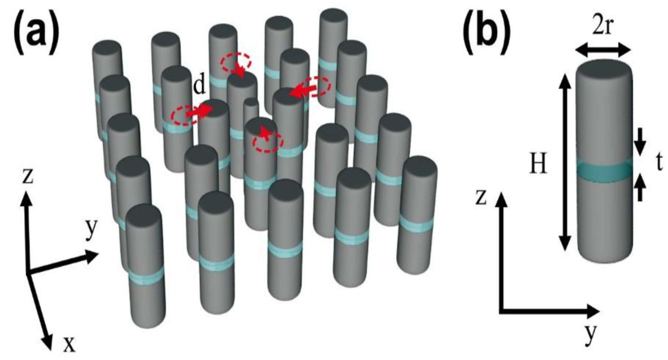
In this paper, we propose a transverse magnetic (TM) polarized two-dimensional (2D) photonic crystal thin silica (SiO2) layered cavity with a high Q factor, small mode volume (Vm), and high confinement factor () in the thin SiO2 layer on a square lattice of silicon rods. The proposed cavity is a possible best candidate for the realization of a silicon-compatible nanolight source.
2. Thin Low-Index Layered Photonic Crystal Cavity Structure
We propose a photonic crystal (PhC) cavity structure consisting of square lattices of dielectric rods, in which a thin SiO
2 layer with thickness of t is sandwiched between the top and bottom silicon layers, as shown in
Figure 1a,b. The total height and radius of each cylinder, and the lattice constant are denoted by H, r, and a, respectively. The central defect cylinder has radius of
rd, and the nearest four cylinders are shifted into the center of the cavity with a distance of d. The refractive indices are 3.48 and 1.47 for Si and SiO
2, respectively, which are the indices for the telecommunication wavelength of 1550 nm. There is a total of 19 × 19 cylinders. For this structure, we calculated the optical properties of the cavity mode and the horizontal SiO
2 slot slab waveguide mode, as well as the quality (
Q) factor, wavelength, mode volumes, and mode profiles using a home-made three-dimensional (3D) finite-difference time-domain (FDTD) code. Perfectly matched layers are used as boundary conditions for all of the directions in the simulations of the cavity mode, and a periodic boundary condition considering the wavevector is used for the y direction, which is the propagation direction in the simulations of the waveguide mode. A grid of 5 nm is used. The proposed rod PhC cavity structure can be fabricated from silicon on insulator substrate using a standard CMOS fabrication process. In addition, by using glutinous substances (e.g., polydimethylsiloxane) [
6,
17], the whole PhC cavity can be detached from the Si wafer and transferred into other photonic structures such as waveguides.
3. Dispersion Curves of Slot Slab Waveguide
First, to determine the total height (
H) of the cylinder for the strong vertical confinement of lights, we investigated the effect of Si slab height on the effective index. We calculated the dispersion curves of a transverse magnetic (TM) Si slab waveguide mode by increasing the height (
H) of the slab, as shown in
Figure 2a. Here, the dominant electric field is aligned in the height direction. When the height is 200 nm (red), the dispersion curve follows the light line for small wavevectors and long wavelengths because of weak vertical confinement in the slab. As the height increases, the dispersion curve approaches the dispersion line of an infinitely thick Si slab waveguide (dotted blue line). By using the dispersion curves of
Figure 2a, we obtain the effective index of the Si slab waveguide mode as a function of the height (
H) for a wavelength of 1550 nm, as shown in
Figure 2b. As height increases, the effective index increases, and when height is larger than 800 nm, the index approaches the bulk index of Si, 3.48. Since the effective index of the slab with a height of 1000 nm is 3.4, which is almost the same value of bulk Si, we chose a total rod height of 1000 nm. In addition, the fabrication of Si rods with a height of 1000 nm can be accomplished conventionally using standard Si CMOS fabrication technology.
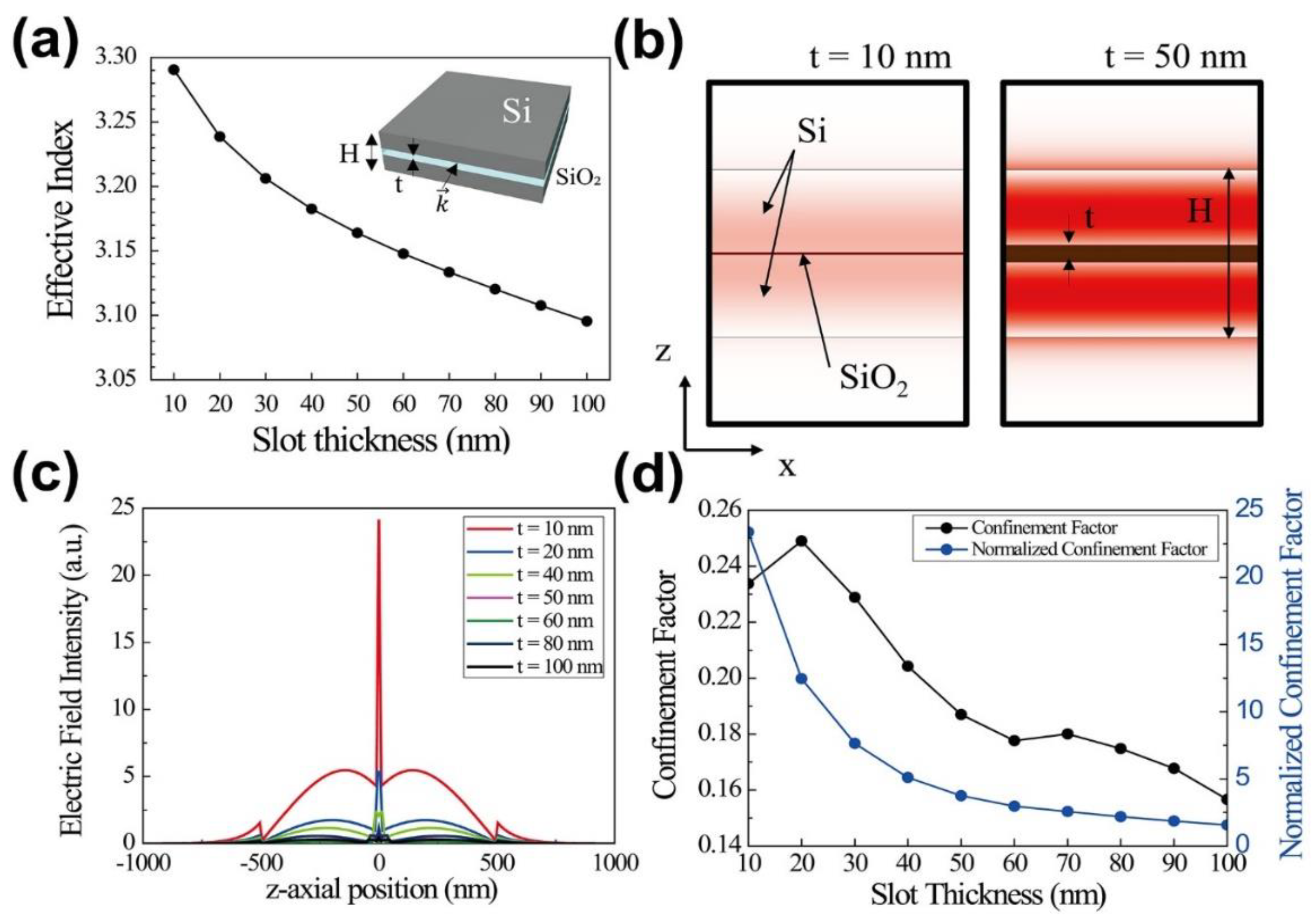
Next, we calculated the effective index of the SiO
2 slot waveguide as a function of slot thickness (
t), as shown in
Figure 3a, where the low-index SiO
2 slot is sandwiched between high-index Si materials at the center of the Si slab with a height (
H) of 1000 nm. Here, a TM-like waveguide mode with the dominant electric field in the vertical direction to the slab is considered. As the slot thickness increases, the effective index decreases monotonically, because the waveguide mode experiences more low-index material (SiO
2) than high-index material (Si). For example, the effective indexes in the slots with thicknesses of 10 nm and 50 nm are 3.29 and the 3.16, respectively.
Figure 3b shows the strong confinement of the z-directional electric field intensity profiles for the waveguides of the 10-nm and 50-nm thick slots, where the total height is fixed at 1000 nm. The electric field is more strongly confined within the 10-nm thick slot than in the slot thickness of the 50-nm thick slot.
In the electric field intensity line graphs of
Figure 3c for different slot thickness, the high electric field intensity is strongly confined in the slot region, as shown in the mode profiles of
Figure 3b. In addition, the 10-nm thick slot shows the highest electric field intensity in the slot, and the peak intensity decreases with increasing slot thickness. Here, the electric field intensity is normalized by the total electric field energy of the waveguide mode for each slot structure. The electric field intensity is related to enhance the emission of the rare earth emitter embedded in the low-index material by the Purcell effect.
In addition to the electric field intensity, the confinement factor denoted by Equation (1) is also considered for the proposed structure as a candidate nanolaser, because the confinement factor can yield an effective modal gain by Equation (2). Therefore, we calculated the confinement factor by estimating the ratio of the entire electric field density and slot area density. This confinement factor represents the density of the fields in the slot area [
18,
19].
where
gmod and
are the modal gain and bulk material gain, respectively.
Figure 3d shows the confinement factor (black) and the normalized confinement factor (blue) as functions of horizontal slot thickness. The maximum confinement factor of 0.25 is found at the slot thickness 20 nm. However, the normalized confinement factor, which is defined as the ratio of the confinement factor and the slot thickness, is a maximum at a slot thickness of 10 nm. The normalized confinement factor means the averaged electric field intensity over the slot, where the confinement factors are normalized by the whole electric field. In general, because the rare-earth emitter is randomly distributed over the low-index layer, the normalized confinement factor can guarantee better performance as a light-emitting diode for the suggested structure. Depending on the applications, the structure that has a high confinement factor or normalized confinement factor can be chosen. In the rest of this paper, we use a horizontal slot thickness of 10 nm at a fixed rod height of 1000 nm for the high confinement of the cavity mode in the horizontal slot, which will be used as gain materials, including rare-earth dopants.
4. Design of Photonic Crystal Cavity Mode
We designed a 2D photonic crystal by placing cylinders with square lattices consisting of Si and a thin SiO
2 layer, where the total height (
H) and SiO
2 thickness (
t) of each cylinder were 1000 nm and 10 nm, respectively. The lattice constant (
a) and radius (
r) of the cylinder are set to 500 nm and 125 nm, respectively, to achieve a maximum photonic bandgap based on the 3D plane wave expansion (PWE) method. In the calculations of the bandgap, we used a superlattice of the stacked structure of air and a 2D rod-type photonic crystal layer. The photonic band diagram of
Figure 4a shows that the target wavelength of 1550 nm (1216 THz) is positioned in the photonic bandgap of the proposed structure. The photonic band diagram was obtained by the 3D PWE method. The
Q factor and electric field distributions of a cavity mode were obtained by using FDTD analysis. To induce a cavity mode, we reduced the radius of a cylinder at the center and obtained a fundamental cavity mode at wavelengths of 1549 nm, 1568 nm, and 1612 nm when the defect radius (
rd) was 80 nm, 85 nm, and 90 nm, respectively (
Figure 4b–d). The highest quality factor (
Q factor) is 4900 in the structure, with an
rd of 90 nm.
To increase the
Q factor further, we suppressed the vertical radiation loss of the cavity by shifting the four nearest neighborhood cylinders into the center defect and changing the mode profiles slightly [
20], as shown in
Figure 5a. As the nearest cylinders shift into the center and the distance changes from 10 nm to 100 nm, the resonant wavelength of the cavity mode blue-shifts 1568 nm to 1509 nm because of the decrease in the mode volume, as shown in
Figure 5c. In contrast, the
Q factor has the highest value of 15,000 when
rd and the shifted distance (d) are 90 nm and 60 nm, respectively, and the corresponding wavelength is 1537 nm.
Figure 5b shows the horizontal and vertical mode profiles in the cavity with
rd = 90 nm and
d = 60 nm. The mode is horizontally well confined in the defect cylinder by the photonic bandgap. As expected from the slot waveguide mode profile of
Figure 3b, the electric field is strongly confined in the low-index thin SiO
2 layer, as shown in the inset of
Figure 5b.
Based on the optimized cavity structure, we investigated the emission enhancement of rare-earth dopants that can be embedded in the thin SiO
2 layer by calculating the Purcell factor. The magnitude of the enhancement is given by the following Purcell factor
when the emitter is placed at the intensity maximum of the mode profile [
21], which corresponds to the proposed cavity. The dopant emitter is placed at the 10-nm thick SiO
2 layer of the center cylinder, in which the spatial overlap between the cavity mode and the emitter can be achieved:
where
is the resonant wavelength of the cavity,
is the refractive index of silica,
V is the mode volume, and
Q is the
Q factor.
To calculate the Purcell factor, we need to know the mode volume of the cavity mode. The mode volume can be calculated by under the following formula [
13]:
where
is the permittivity as a function of the radial direction, and
is the electric field of the cavity mode as a function of the radial direction at the cavity center.
On the other hand, in case the maximum electric field is found in a low-index region, the mode volume can be represented as a normalized unitless effective mode volume [
22]. The normalized mode volume is defined as follows:
where
is the position of the maximum electric field. Therefore,
) is
.
is the maximum permittivity of the radial direction. The normalized unitless effective mode volume is 0.64.
For the optimized cavity structure with rd = 90 nm and d = 60 nm, the mode volume is obtained as = 0.01 μm3 (= 0.0089 μm3), where, is 1537 nm and is 1.48. By using a wavelength of 1537 nm, Q factor of 15,000, and refractive index of SiO2 of 1.48, the Purcell factor is 127,000. The large Purcell factor means that the proposed cavity structure can enhance the emission of the rare-earth dopants in the low-index layer and will be useful as a silicon-compatible nanolight source.
In order to consider mechanically stable, practical devices in the low-index dielectric substrate, PDMS (n = 1.396), SiO2 (n = 1.47), we calculated the effects of the substrate on the Q factor for the optimized PhC cavity (r = 120 nm, H = 1000 nm, t = 10 nm, rd = 90 nm, d = 60 nm). The Q factor decreases to 750 and 490 for PDMS and SiO2 due to leakage loss into the substrate, respectively. In order to overcome leakage loss, the height of the rod can be increased by increasing the distance between the high-intensity region, SiO2 layer, and substrate. When the height of the rod becomes 1400 nm and the distance from the SiO2 layer to the substrate increases to 895 nm, the Q factor is largely improved to 2200 and 870 for PDMS and SiO2 substrate, respectively.
5. Conclusions
In conclusion, we propose a high-Q photonic crystal cavity with a thin low-index SiO2 layer sandwiched at the center of the silicon cylinders. Owing to the optical property of the TM waveguide slot mode, the electric field is strongly confined at the 10-nm thick low-index layer with a confinement factor of 0.23, where rare-earth dopants with telecommunication emission wavelengths can be embedded. By constructing photonic crystals with square lattices of silicon cylinders with a height of 1000 nm, lattice constant of 500 nm, cylinder radius of 125 nm, and thin low-index layer thickness of 10 nm, the photonic bandgap, including the telecommunication wavelength, can be built. By decreasing the radius of the center cylinder to 90 nm and shifting the four nearest cylinders into the center over a distance of 60 nm, we can optimize the cavity mode with a resonant wavelength of 1537 nm, high Q factor of 15,000, and mode volume of 0.01 μm3 = 0.0089μm3. If an emitter is embedded at the low-index layer, a high Purcell factor is estimated as 127,000, owing to strong electric field localization in the low-index layer. We believe that the design of the proposed cavity based on the silicon cylinder and SiO2 layer will be useful in the development of a silicon-based nanolight source, which is urgently required for the CMOS compatible photonic integrated circuit.
Due to spatial spreading, the ion implants of rare-earth dopants have difficulties applying to the thin SiO
2 layer of the proposed rod-type photonic crystal structure. The proposed structure can be fabricated by radio frequency confocal magnetron sputtering, and the rare-earth doped thin SiO
2 layer also can be prepared by the co-sputtering of three targets: Si, SiO
2, and the oxides of rare-earth materials [
23,
24].


