Influence of Quantum-Well Number and an AlN Electron Blocking Layer on the Electroluminescence Properties of AlGaN Deep Ultraviolet Light-Emitting Diodes

Abstract
1. Introduction
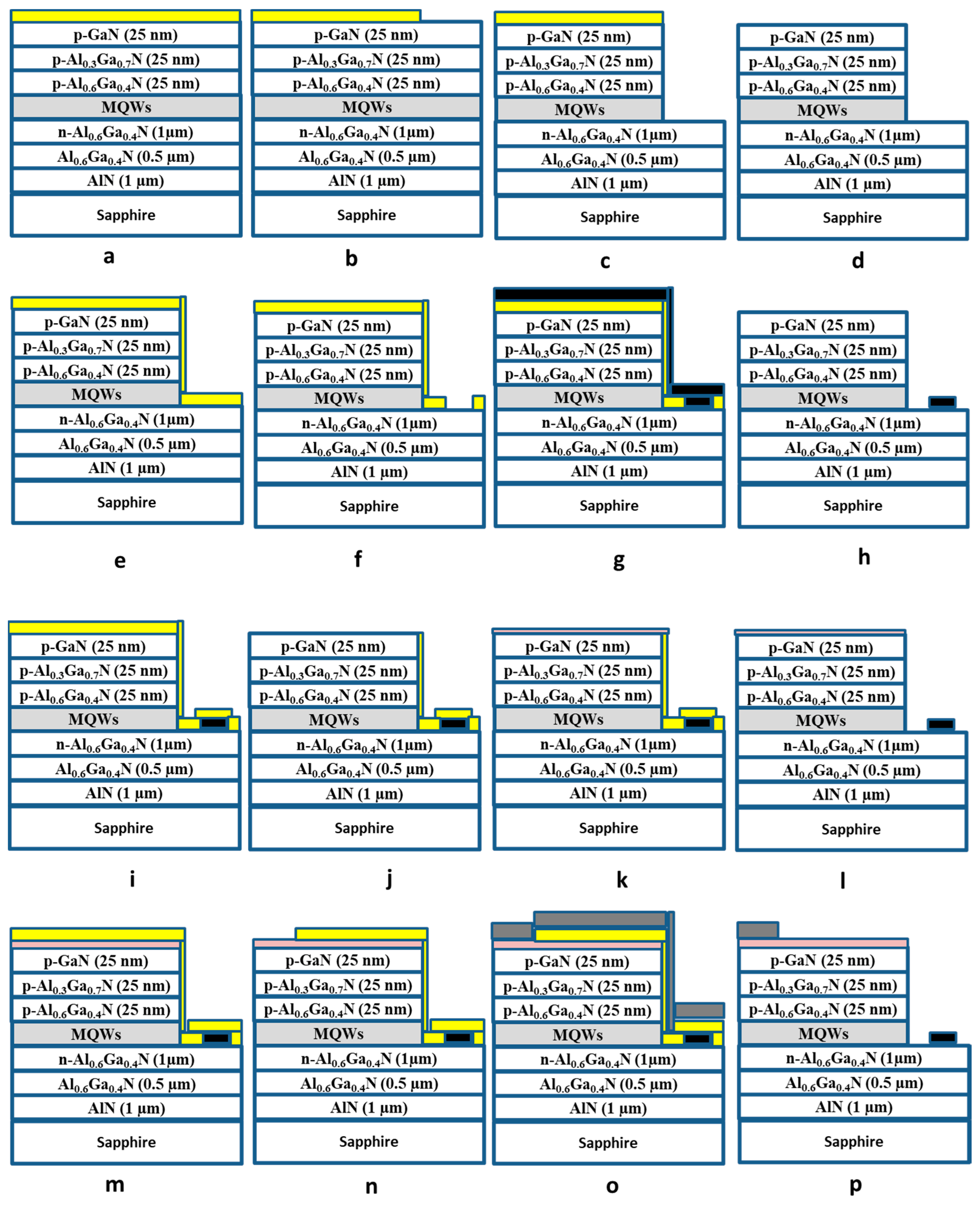
2. Experiment
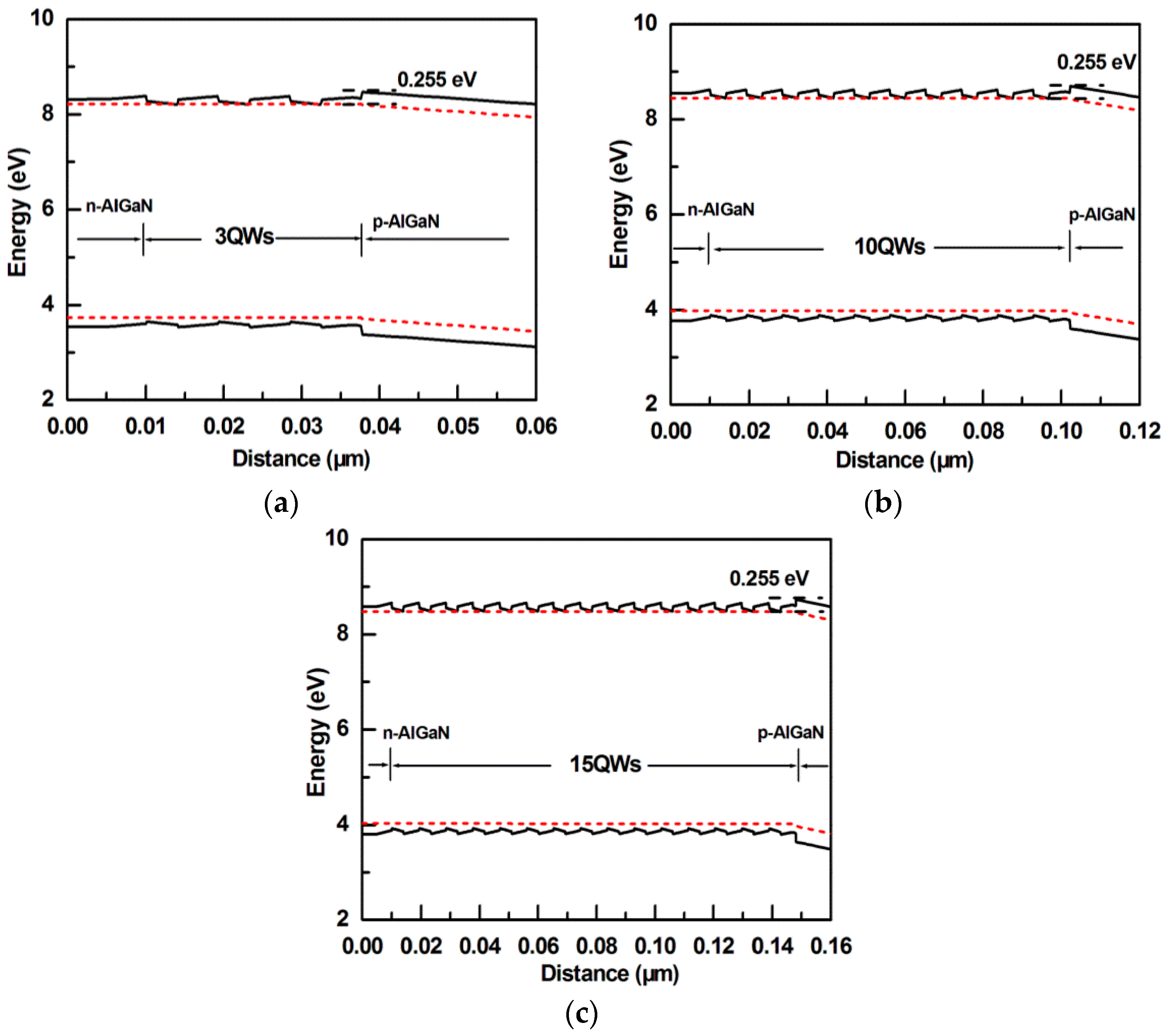
3. Experimental Results
4. Simulation and Discussion
5. Conclusions
Author Contributions
Funding
Acknowledgments
Conflicts of Interest
References
- Li, D.; Jiang, K.; Sun, X.; Guo, C. AlGaN photonics: Recent advances in materials and ultraviolet device. Adv. Opt. Photonics 2018, 10, 43–110. [Google Scholar] [CrossRef]
- Chitnis, A.; Sun, J.; Mandavilli, V.; Pachipulusu, R.; Wu, S.; Gaevski, M.; Adivarahan, V.; Zhang, J.P.; Khan, M.A.; Sarua, A.; et al. Self-heating effects at high pump currents in deep ultraviolet light-emitting diodes at 324 nm. Appl. Phys. Lett. 2002, 81, 3491–3493. [Google Scholar] [CrossRef]
- Zhang, J.C.; Zhu, Y.H.; Egawa, T.; Sumiya, S.; Miyoshi, M.; Tanaka, M. Influence of pulse width on electroluminescence and junction temperature of AlInGaN deep ultraviolet light-emitting diodes. Appl. Phys. Lett. 2008, 92, 191917. [Google Scholar] [CrossRef]
- Du, C.; Jing, L.; Jiang, C.; Liu, T.; Pu, X.; Sun, J.; Li, D.; Hu, W. An effective approach to alleviating the thermal effect in microstripe array-LEDs via the piezo-phototronic effect. Mater. Horiz. 2018, 5, 116–122. [Google Scholar] [CrossRef]
- Li, D.; Sun, X.; Song, H.; Li, Z.; Chen, Y.; Jiang, H.; Miao, G. Realization of a High-Performance GaN UV Detector by Nanoplasmonic Enhancement. Adv. Mater. 2012, 24, 845–849. [Google Scholar] [CrossRef] [PubMed]
- Nakarmi, M.L.; Kim, K.H.; Khizar, M.; Fan, Z.Y.; Lin, J.Y.; Jiang, H.X. Electrical and optical properties of Mg-doped Al0.7Ga0.3N alloys. Appl. Phys. Lett. 2005, 86, 092108. [Google Scholar] [CrossRef]
- Kinoshita, T.; Obata, T.; Yanagi, H.; Inoue, S. High p-type conduction in high-Al content Mg-doped AlGaN. Appl. Phys. Lett. 2013, 102, 012105. [Google Scholar] [CrossRef]
- Kim, H.K.; Seong, T.Y.; Adesida, I.; Tang, C.W.; Lau, K.M. Low-resistance Pt/Pd/Au ohmic contacts to p-type AlGaN. Appl. Phys. Lett. 2004, 84, 1710–1712. [Google Scholar] [CrossRef]
- Huang, X.; Du, C.; Zhou, Y.; Jiang, C.; Pu, X.; Liu, W.; Hu, W.; Chen, H.; Wang, Z.L. Piezo-Phototronic Effect in a Quantum Well Structure. ACS Nano 2016, 10, 5145–5152. [Google Scholar] [CrossRef]
- Yang, G.F.; Xie, F.; Dong, K.X.; Chen, P.; Xue, J.J.; Zhi, T.; Tao, T.; Liu, B.; Xie, Z.L.; Xiu, X.Q.; et al. Design of deep ultraviolet light-emitting diodes with staggered AlGaN quantum wells. Phys. E Low-Dimens. Syst. Nanostruct. 2014, 62, 55–58. [Google Scholar] [CrossRef]
- Miyake, H.; Lin, C.-H.; Tokoro, K.; Hiramatsu, K. Preparation of high-quality AlN on sapphire by high-temperature face-to-face annealing. J. Cryst. Growth 2016, 456, 155–159. [Google Scholar] [CrossRef]
- Sun, M.; Zhang, J.; Huang, J.; Li, X.; Wang, L.; Liu, X.; Wang, J.; Xu, K. Influence of thickness on strain state and surface morphology of AlN grown byHVPE. J. Semicond. 2016, 37, 123001. [Google Scholar] [CrossRef]
- Sun, X.; Li, D.; Chen, Y.; Song, H.; Jiang, H.; Li, Z.; Miao, G.; Zhang, Z. In situ observation of two-step growth of AlN onsapphire using high-temperature metal–organic chemical vapour deposition. CrystEngComm 2013, 15, 6066–6073. [Google Scholar] [CrossRef]
- Jiang, K.; Sun, X.; Ben, J.; Jia, Y.; Liu, H.; Wang, Y.; Wu, Y.; Kai, C.; Li, D. The defect evolution in homoepitaxial AlN layers grown by high-temperature metal–organic chemical vapor deposition. CrystEngComm 2018, 20, 2720–2728. [Google Scholar] [CrossRef]
- Zhang, L.; Xu, F.; Wang, J.; He, C.; Guo, W.; Wang, M.; Sheng, B.; Lu, L.; Qin, Z.; Wang, X.; et al. High-quality AlN epitaxy on nano-patterned sapphire substrates prepared by nano-imprint lithography. Sci. Rep. 2016, 6, 35934. [Google Scholar] [CrossRef] [PubMed]
- Nagasawa, Y.; Hirano, A. A Review of AlGaN-Based Deep-Ultravioletht-Emitting Diodes on Sapphire. Appl. Sci. 2018, 8, 1264. [Google Scholar] [CrossRef]
- Kim, J.; Choi, U.; Pyeon, J.; So, B.; Nam, O. Deep-Ultraviolet AlGaN/AlN Core-Shell Multiple Quantum Wells on AlN Nanorods via Lithography-Free Method. Sci. Rep. 2018, 8, 935. [Google Scholar] [CrossRef]
- Kuo, Y.-K.; Chang, Y.-A. Effects of electronic current overflow and inhomogeneous carrier distribution on InGaN quantum-well laser performance. IEEE J. Quantum Electron. 2004, 40, 437–444. [Google Scholar]
- Han, D.-P.; Kim, H.; Shim, J.-I.; Shin, D.-S.; Kim, K.-S. Influence of carrier overflow on the forward-voltage characteristics of InGaN-based light-emitting diodes. Appl. Phys. Lett. 2014, 105, 191114. [Google Scholar] [CrossRef]
- Zhang, J.C.; Zhu, Y.H.; Egawa, T.; Sumiya, S.; Miyoshi, M.; Tanaka, M. Suppression of the subband parasitic peak by 1nm i-AlN interlayer in AlGaN deep ultraviolet light-emitting diodes. Appl. Phys. Lett. 2008, 93, 131117. [Google Scholar] [CrossRef]
- Fischer, A.J.; Allerman, A.A.; Crawford, M.H.; Bogart, K.H.A.; Lee, S.R.; Kaplar, R.J.; Chow, W.W.; Kurtz, S.R.; Fullmer, K.W.; Figiel, J.J. Room-temperature direct current operation of 290 nm light-emitting diodes with milliwatt power levels. Appl. Phys. Lett. 2004, 84, 3394–3396. [Google Scholar] [CrossRef]
- Choi, H.-S.; Zheng, D.-G.; Kim, H.; Shim, J.-I.; Shin, D.-S. Effects of the number of quantum wells on the performance of near-ultraviolet light-emitting diodes. J. Korean Phys. Soc. 2015, 66, 1554–1558. [Google Scholar] [CrossRef]
- Kim, D.-J.; Moon, Y.-T.; Song, K.-M.; Choi, C.-J.; Ok, Y.-W.; Seong, T.Y.; Park, S.-J. Structural and optical properties of InGaN/GaN multiple quantum wells: The e!ect of the number of InGaN/GaN pairs. J. Cryst. Growth 2000, 221, 368–372. [Google Scholar] [CrossRef]
- Pan, C.-C.; Lee, C.-M.; Liu, J.-W.; Chen, G.-T.; Chyi, J.-I. Luminescence efficiency of InGaN multiple-quantum-well ultraviolet light-emitting diodes. Appl. Phys. Lett. 2004, 4, 5249–5251. [Google Scholar] [CrossRef]
- Kolbe, T.; Stellmach, J.; Mehnke, F.; Rothe, M.A.; Kueller, V.; Knauer, A.; Einfeldt, S.; Wernicke, T.; Weyers, M.; Kneissl, M. Efficient carrier-injection and electron-confinement in UV-B light-emitting diodes. Phys. Status Solidi A 2016, 213, 210–214. [Google Scholar] [CrossRef]
- So, B.; Kim, J.; Shin, E.; Kwak, T.; Kim, T.; Nam, O. Efficiency Improvement of Deep-Ultraviolet Light Emitting Diodes with Gradient Electron Blocking Layers. Phys. Status Solidi A 2018, 215, 1700677. [Google Scholar] [CrossRef]
- Hirayama, H.; Tsukada, Y.; Maeda, T.; Kamata, N. Marked Enhancement in the Efficiency of Deep-Ultraviolet AlGaN Light-Emitting Diodes by Using a Multiquantum-Barrier Electron Blocking Layer. Appl. Phys. Express 2010, 3, 031002. [Google Scholar] [CrossRef]
- Lu, L.; Ding, G.G.; Zhang, Y.; Liu, Y.H.; Xu, F.J. Improved Performance of AlGaN-Based Deep-Ultraviolet Light-Emitting Diodes using modulated-taper design for p-AlGaN layer. Semicond. Sci. Technol. 2018, 33, 0350008. [Google Scholar] [CrossRef]


| LEDs | EBL | QW Number |
|---|---|---|
| A | no | 5 |
| B | no | 10 |
| C | no | 40 |
| D | 1 nm AlN | 5 |
| Layers | Electron Concentration(cm−3) | Hole Concentration (cm−3) |
|---|---|---|
| p-GaN | 5 × 10¹⁸ | |
| p-Al0.3Ga0.7N | 5 × 10¹⁷ | |
| p-Al0.6Ga0.4N | 5 × 10¹⁷ | |
| n-Al0.6Ga0.4N | 5 × 10¹⁸ |
| Layers | Thickness (nm) |
|---|---|
| p-GaN | 25 |
| p-Al0.3Ga0.7N | 25 |
| p-Al0.6Ga0.4N | 25 |
| i-Al0.92Ga0.08N | 1 |
| Well | 3 |
| Barrier | 5 |
| n-Al0.6Ga0.4N | 1000 |
© 2018 by the authors. Licensee MDPI, Basel, Switzerland. This article is an open access article distributed under the terms and conditions of the Creative Commons Attribution (CC BY) license (http://creativecommons.org/licenses/by/4.0/).
Share and Cite
Tan, S.; Zhang, J.; Egawa, T.; Chen, G. Influence of Quantum-Well Number and an AlN Electron Blocking Layer on the Electroluminescence Properties of AlGaN Deep Ultraviolet Light-Emitting Diodes. Appl. Sci. 2018, 8, 2402. https://doi.org/10.3390/app8122402
Tan S, Zhang J, Egawa T, Chen G. Influence of Quantum-Well Number and an AlN Electron Blocking Layer on the Electroluminescence Properties of AlGaN Deep Ultraviolet Light-Emitting Diodes. Applied Sciences. 2018; 8(12):2402. https://doi.org/10.3390/app8122402
Chicago/Turabian StyleTan, Shuxin, Jicai Zhang, Takashi Egawa, and Gang Chen. 2018. "Influence of Quantum-Well Number and an AlN Electron Blocking Layer on the Electroluminescence Properties of AlGaN Deep Ultraviolet Light-Emitting Diodes" Applied Sciences 8, no. 12: 2402. https://doi.org/10.3390/app8122402
APA StyleTan, S., Zhang, J., Egawa, T., & Chen, G. (2018). Influence of Quantum-Well Number and an AlN Electron Blocking Layer on the Electroluminescence Properties of AlGaN Deep Ultraviolet Light-Emitting Diodes. Applied Sciences, 8(12), 2402. https://doi.org/10.3390/app8122402