Article

Novel Common-Mode Current Suppression Method in Transformerless PV Grid-Connected System

College of Automation, Hangzhou Dianzi University, Hangzhou 310018, China
*
Author to whom correspondence should be addressed.
Appl. Sci. 2018, 8(11), 2072; https://doi.org/10.3390/app8112072
Submission received: 12 September 2018 / Revised: 19 October 2018 / Accepted: 25 October 2018 / Published: 26 October 2018
(This article belongs to the Special Issue Control and Protection Issues of Grid-Tied Photovoltaic System)

Abstract

:
The existence of high-frequency components in common-mode (CM) current would reduce the stability of a non-isolated PV grid-connected system. It has great impacts on the output power quality when the generated power from PV is low. The method of single CM inner loop in suppressing the high-frequency components has poor effect. Based on the CM equivalent circuit model and the cause analysis of the CM current, a novel dual CM inner loops method is proposed to restrain the high-frequency components in CM current. This method not only meets the grid connection demand of CM current, but also overcomes the high frequency resonant problem. Furthermore, the high-frequency components in CM current from the outer parasitic circuit are substantially reduced. Finally, the proposed method is verified by simulation and experimental results.

1. Introduction

The PV grid-connected inverter is an indispensable part of grid connected PV power generation systems. It should be pointed out that the isolated transformers of line frequency or high frequency are used as inverters in the traditional PV system. The line frequency transformer is installed on the ac output side, which is bulky and inconvenient to install and decreases the efficiency of the system. Although the high-frequency transformer reduces the size of PV system, it is installed on the dc side, which increases the complexity of main circuits, reduces the system stability, and affects the system efficiency. To overcome these shortcomings and improve the efficiency of PV system, the transformerless inverters are widely used in the residential PV system with small capacities [1]. Although the volumes have been greatly reduced in the transformerless inverter, the efficiency has been improved, and the costs has been decreased. The parasitic capacitance, which is between the PV modules and the ground as well as the grid, forms the CM circuit due to the lack of galvanic isolation between the PV systems and grids. Therefore, the CM current in the PV system has a negative influence on the safety of the whole system.
At present, there are two main methods to suppress the CM currents: (1) An inverter topology with the characteristics of CM current suppression and an improved modulation mode are adopted. A Space Vector Pulse Width Modulation (SVPWM) method is proposed to suppress the CM current [2]. The full bridge topology, with dc bypass and full bridge topology with ac bypass [3], and the topology with CM current suppression [4] have a decoupling effect on the grid side and dc side and ensure the constant CM voltages during the freewheeling period of PWM method. The Single-phase clamp topology [5] can also suppress CM currents. (2) The Electro Magnetic Interference (EMI) filter is added to the ac side [6]. The impedance in the CM loop can be increased, which inhibits the CM current flowing into the grid and effectively suppresses the CM loop current. The current standard for the grids requires that the CM current should be less than 30 mA [7]. Based on the above two methods, the CM current can be generally suppressed to be less than 30 mA. However, there are many high frequency components in the CM current flowing through the power grid; the power quality is decreased and the great electromagnetic interference to the inverter is introduced such that the stability of the whole system is reduced and the internal lifetime of the inverter is shortened. To prevent the electric shock accident due to excessive CM current, the leakage protection device is installed on the output side of inverters. Because of the changes in the external environment, especially for the parasitic capacitance value change on rainy days, the change of the CM current in the high frequency component will lead to the action of leakage protection device, which makes the system stop working and often brings unnecessary losses to the users. The distributed PV system will be widely used in future. If many grid connected and residential PV systems stop working at the same time, the voltage drop of the grid will appear such that the stability of the power grid will be greatly reduced.
In recent years, some scholars have proposed to set CM internal loop at the output side of the system to suppress CM current. In [8], a CM internal loop is proposed by connecting the midpoint of ac side voltage to the dc side voltage point. In [9], a new modulation method is proposed for optimally controlling the power switches of transformerless single-phase full-bridge PV inverters to reduce CM current. In [10], the RC absorption branch is added between the output terminal and the dc negative bus to form a single CM internal loop. However, there is no further analysis of CM current in [8,9,10], and there is no comparative analysis of the effect of CM internal loop on the high frequency component of the CM current. Furthermore, it is easy to produce high frequency resonance in the CM circuit by using the single CM internal loop method so that the large CM current of the resonant frequency will be produced.
In this paper, the CM equivalent circuit is used to analyze the high frequency components of the CM currents. For the high frequency component in CM currents, a method of constructing a dual CM internal loop to suppress the high frequency component of CM currents is proposed. This method does not change the original topology, and the parameter tuning is simple. The simulation results show that the high frequency components of the CM currents can be effectively suppressed by using the proposed method. Finally, the experimental results show that the proposed method has a significant effect on suppressing the high frequency components in the CM currents.

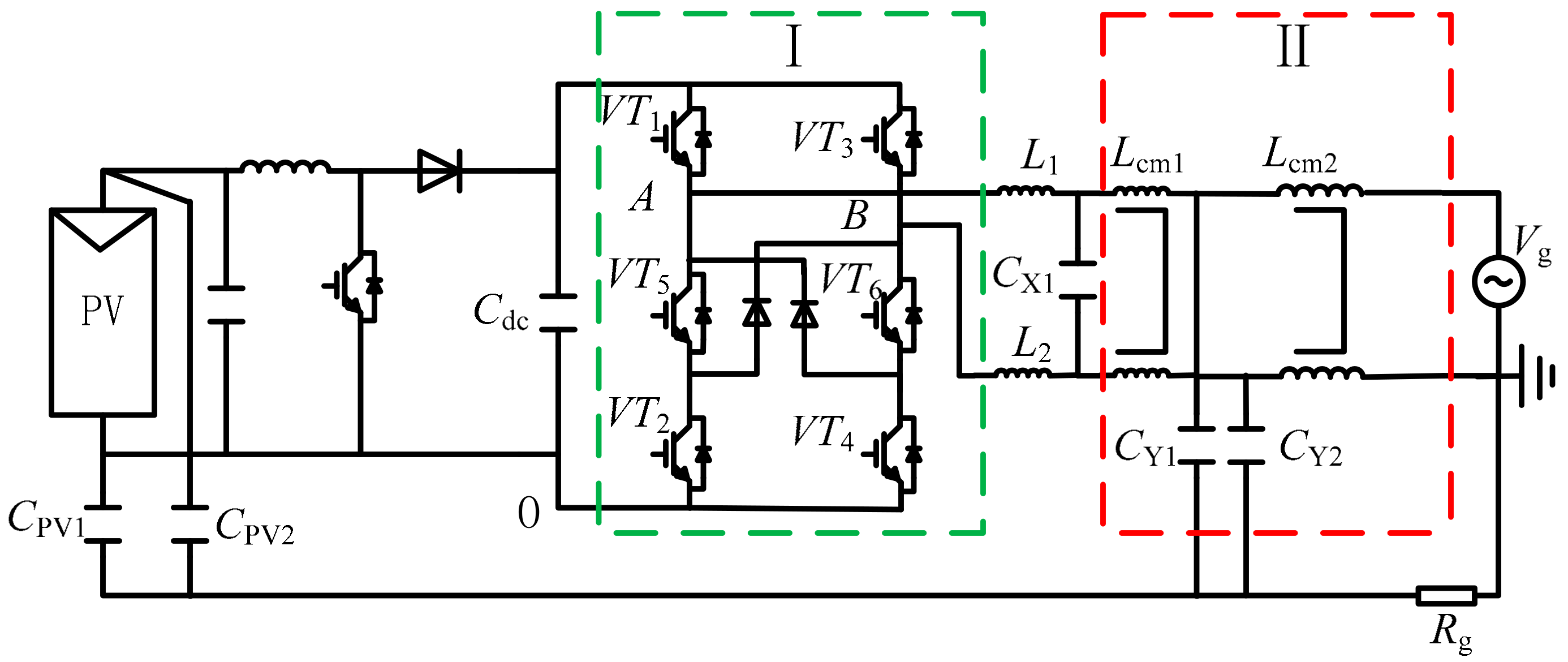
2. Analysis of the CM Current of Non-Isolated Grid-Connected PV System

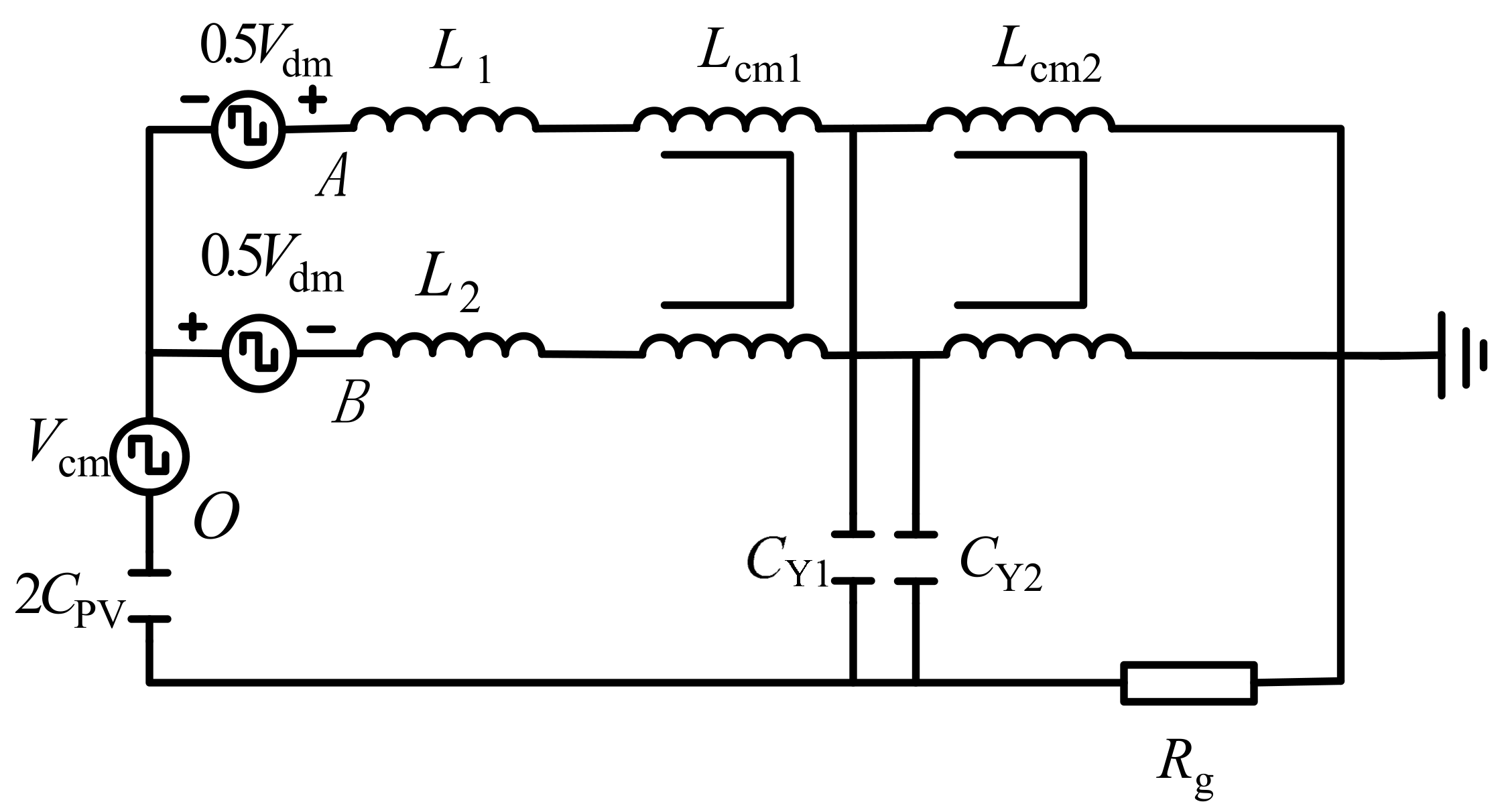
2.1. Analysis of CM Loop Models

In the current market, the distributed residential grid-connected PV systems that have the characteristic of non-isolation and low power include two stages with Boost converter and single-phase inverter [11], as shown in Figure 1. In this system, the Boost circuit mainly completes the MPPT function. When the dc bus voltage Vdc is controlled at a constant value, the output side of the front Boost circuit can be equivalent to a voltage source. The inverter circuit completes the conversion from dc to ac, and the topology with the function of CM current suppression is usually adopted [12].
In Figure 1, the single-phase PV grid connected system with two stages uses the H6 topology shown in the Box I of the Figure 1. This H6 topology embeds two unidirectional freewheel units into the midpoint of a full bridge inverter, which provide novel freewheel paths and separate battery cells form a grid during free wheeling time. Body diodes with poor performance of active switches are not used so it achieves higher efficiency. Meanwhile, split capacitors are not needed as in topologies with dc bypass structure [13]. In addition to the use of LC filter, the EMI filter with Lcm1, CY1, CY2, and Lcm2 is added on the output side shown in Box II of the figure. According to the definitions of the CM voltage and the differential mode voltage, the inverter CM voltage Vcm and differential-mode voltage Vdm can be obtained as:
V cm = 0.5 ( V AO + V BO )
V dm = V AO V BO
thus
V AO = V cm + 0.5 V dm
V BO = V cm 0.5 V dm
In this paper, the high frequency components in the CM current are considered. Therefore, in the CM equivalent circuit, the influence of the grid voltage on the CM circuit is neglected. According to Equations (3) and (4), the CM equivalent circuit of two stages PV grid-connected systems is shown in Figure 2, where CPV is the equivalent parasitic capacitance.
In Figure 2, the CM inductance is located in the differential mode branch. The CM inductance has no influence on the differential signal, therefore, it can be moved to the CM branch. Figure 3 shows the simplified CM equivalent circuit.
By using the principle of circuit equivalent, the differential mode circuit is equivalently transformed and the branch impedance is calculated. The simplest CM equivalent circuit is shown in Figure 4.
In Figure 4, Z is the equivalent impedance of the CM circuit and Vdm-t is the equivalent differential-mode voltage, expressed as:
Z = j ω L 1 2 + j ω L cm 1 + 1 2 j ω C PV + 1 j ω C 1 + 1 / Z 1
V dm - t = V dm L 1 L 2 2 ( L 1 + L 2 )
where ω is the angular frequency.
Z1, C1, and L1-2 are derived as below:
Z 1 = j ω L cm 2 + R g
C 1 = C Y 1 + C Y 2
L 1 2 = L 1 L 2 / ( L 1 + L 2 )
According to Figure 4, the total voltage of the CM voltage loop Vcm-t is derived as:
V cm - t = V cm + V dm L 1 L 2 2 ( L 1 + L 2 )
It is assumed that L1 = L2. The CM loop voltage Vcm-t can be depicted as:
V cm - t = V cm = 0.5 ( V AO + V BO )

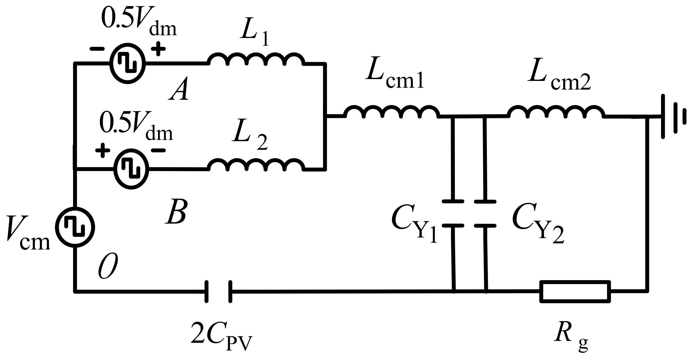
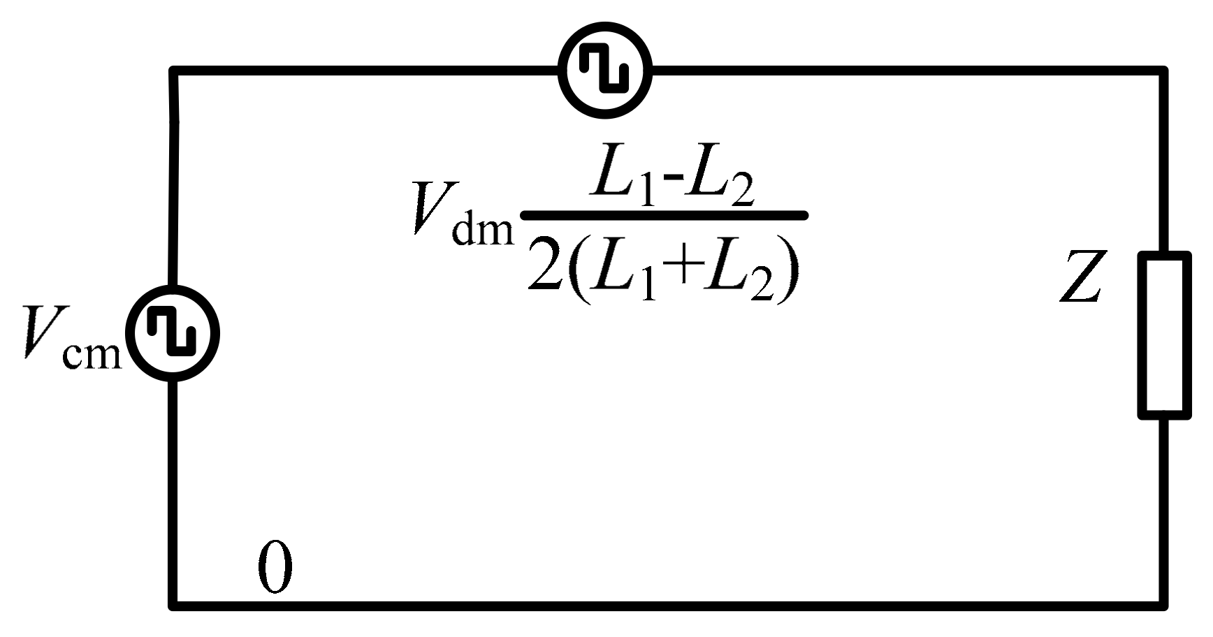
2.2. Analysis of CM Current

Taking the topology shown in Figure 1 as an example, the main components of the CM current are analyzed. The main components of CM current are analyzed from three aspects of CM equivalent circuit, i.e., the CM equivalent model, the modulation of H6 inverter and the load. This section focuses on the generation principle of the high frequency components.
The topology with CM suppression capability under ideal conditions can keep the CM voltage as constant. Therefore, there should be no harmonics of modulation frequency. However, the inconsistency of the dynamic process during the opening and closing of the switching device or the inconsistency of the switching device driving signal leads to the change of CM voltages.
For example, in Figure 1, the bridge of H6 in the positive half cycle modulation process may cause VT4 to be turned off before VT1 due to the inconsistency of dynamic process or of the driving signal. Hence, according to Equation (11), Vcm-t can be depicted as:
V cm - t = V AO + V BO 2 = V dc + 0.5 V dc 2 = 3 V dc 4
where Vcm-t does not return to Vdc/2 until VT1 is turned off, which causes the CM voltage to generate the spike. Conversely, if VT1 is turned off before VT4, Vcm-t will produce a sudden change of Vdc/4. In the worst case, the frequency of CM voltage is the same as the modulation frequency of the inverter bridge.
The circuit resonance caused by the mode transformation of the inverter bridge makes the CM voltage fluctuate. The inverter adopts the PWM mode; therefore, the CM voltage contains the harmonic of each order. Some specific harmonic makes the impedance of the CM equivalent circuit be pure resistance, or makes the local LC branch to be pure resistance, which will lead to resonance. It can be seen from Equation (5) that the impedance of the CM equivalent circuit is lower in the vicinity of the resonant frequency than in the frequency section of non-resonance, which leads to the larger CM current with the same CM voltage at the resonant frequency.
From Equations (2) and (10), due to the asymmetry of the output filter inductance L1 and L2, it can be concluded that the differential mode voltage of the CM circuit loop with the switching frequency is introduced. It is assumed that the inductance difference of L1 and L2 is 10% [14], therefore, Vcm-t can be depicted as:
V cm - t = V cm + V dm L 1 L 2 2 ( L 1 + L 2 ) = V cm ± 0.025 V dm
Because of the asymmetry of L1 and L2, the fluctuation component of 0.025Vdm is introduced into the CM voltage. The fluctuation component includes the switching frequency component and the line frequency component.
The voltage fluctuation at the output of the PV array resulting from the operation of the Boost circuit causes the CM voltage to fluctuate. Therefore, the CM currents of switching frequency are introduced in the CM circuit loop by these non-ideal factors.
The grid can be regarded as the load of the whole PV system. When the grid voltage is not neglected in the CM loop shown in Figure 2, the total voltage is derived as:
V cm - t = 0.5 ( V AO + V BO ) 0.5 V g
From Equation (14), Vcm-t has the fluctuation component of line frequency and the amplitude is half the amplitude of the grid voltage. Hence, the CM current has a large component of line frequency. In addition, since the inverter uses the PWM modulation, the low-order harmonic components in the CM voltage are inevitably produced. The low-order harmonics cannot be filtered by the passive LC filter and EMI filter. Hence, there is a certain amount of low-order harmonic components in the CM current.
In summary, the CM currents of modulation frequency, of resonant frequency and of line frequency are the main components in the CM circuit loop.

3. Proposed Novel CM Internal Loop Method to Suppression CM Current

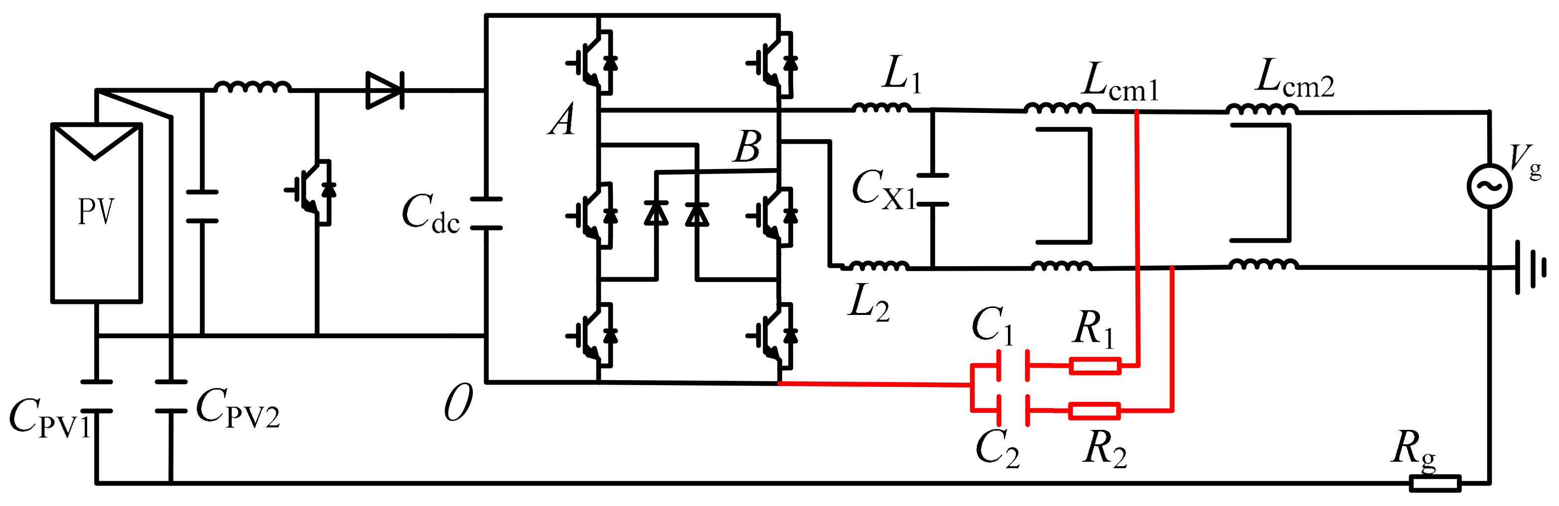
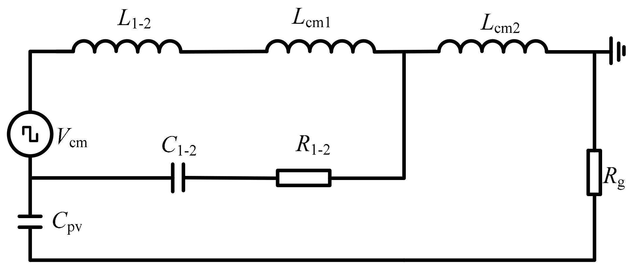
3.1. Traditional Construction of Single CM Internal Loop to Suppress CM Current

To suppress CM current, a grid connected PV system with single CM inner loop, as shown in Figure 5, is constructed. The EMI filter is LCL. However, to form the CM inner loop, the original Y capacitor of the filter is replaced by the RC branch of R1-C1 and R2-C2 so as to be connected to the dc negative bus. Figure 6 is the CM equivalent circuit with a single CM internal loop, where C1-2 and R1-2 are, respectively, given as:
C 1 2 = C 1 + C 2
R 1 2 = R 1 R 2 / ( R 1 + R 2 )

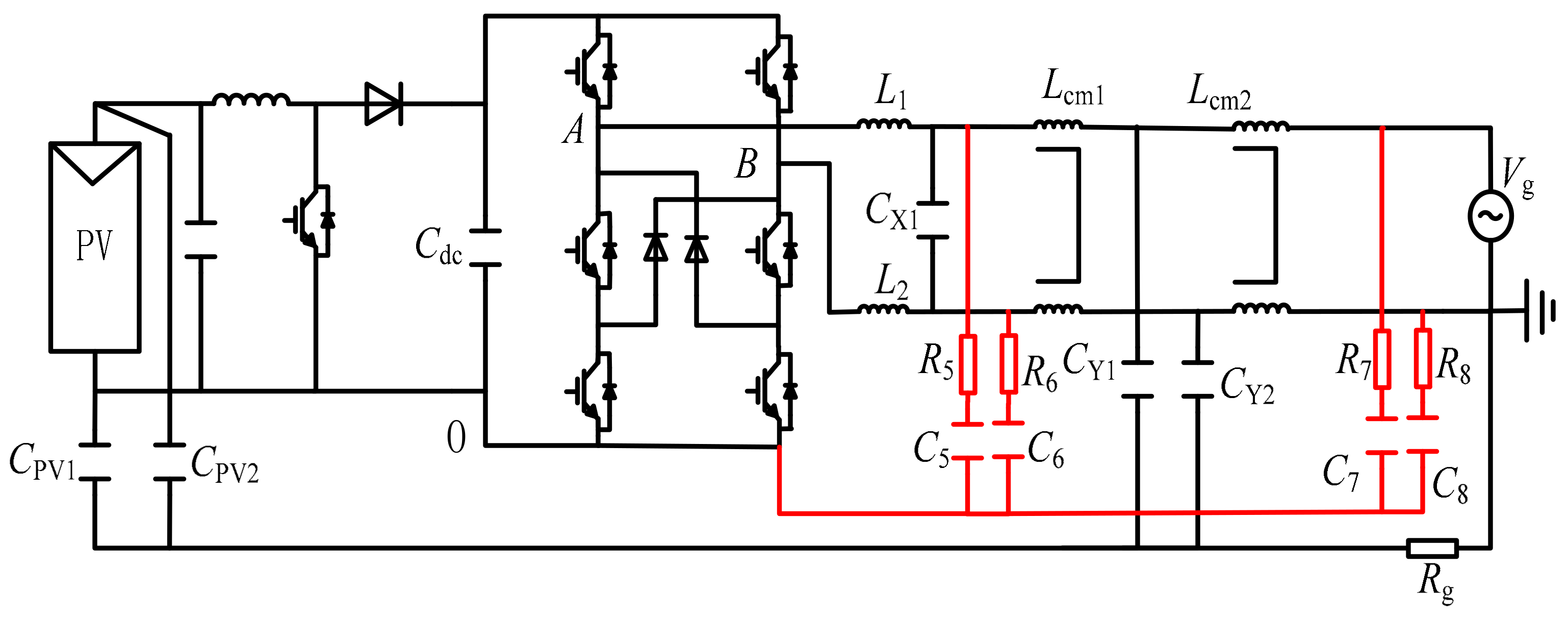
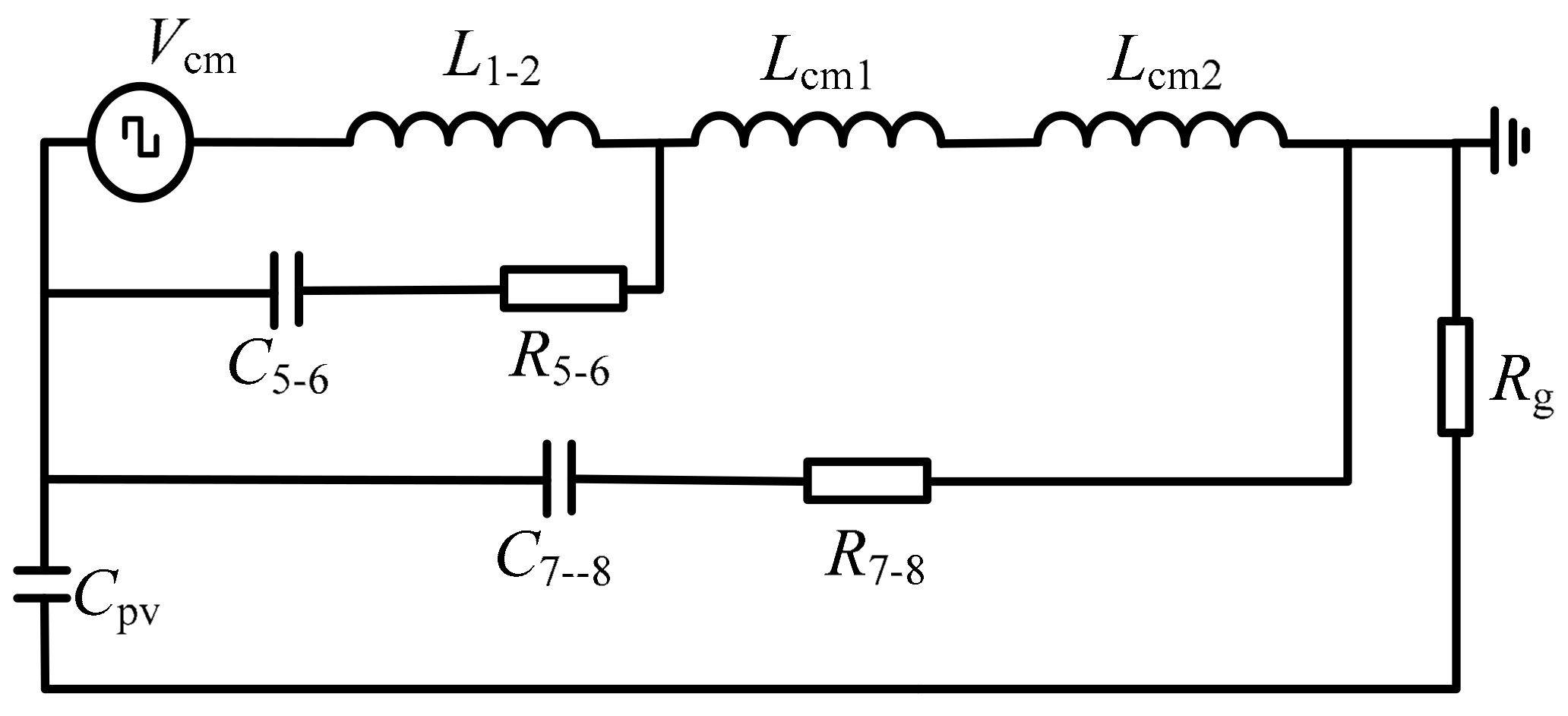
3.2. Proposed Novel Dual CM Internal Loop to Suppress CM Currents

Based on single CM internal loop, this paper proposes to set up the novel RC branch between the EMI filter side and the dc negative bus, which can be named as double CM internal loop, as shown in Figure 7. The R5-C5, R6-C6, R7-C7 and R8-C8 branches are connected to the inverter, the EMI filter side and the dc negative bus side to form a dual CM internal loop, respectively.
In Figure 7, since the value of grounded Y capacitor is usually very small compared with the parasitic capacitance, the Y capacitor of the EMI filter is ignored [15]. Figure 8 shows the CM equivalent circuit with a double CM internal loop, where C5-6, R5-6, C7-8, and R7-8 are described.
C 5 6 = C 5 + C 6
R 5 6 = R 5 R 6 / ( R 5 + R 6 )
C 7 8 = C 7 + C 8
R 7 8 = R 7 R 8 / ( R 7 + R 8 )
For the second order LC circuit, the resonant frequency fres1 and fres2 are derived as [16]:
f res 1 = 1 2 π ( L 1 2 + L cm 1 ) · ( C 1 2 + C PV )
f res 2 = 1 2 π L cm 2 C PV C 1 2 C 1 2 + C PV
Capacitors C1 and C2 should satisfy fres1 and fres2 [8]:
10 f grid f res 1 f sw / 10
3 f res 1 f res 2 f sw / 2
where fgrid is the grid frequency and fsw is the switching frequency of the inverter.
Figure 6 shows the single CM internal loop. Let fres1 = 1.5 kHz and CPV = 0.5 μF. According to the experimental platform, the filter parameters are set as Lcm1 = Lcm2 = 1.3 mH and L1 = L2 = 1 mH. The calculated value of C1 and C2 is 2.88 μF. In practical application, the value of C1 and C2 is 2.7 μF, therefore fres2 ≈ 6.5 kHz, which meet the requirements of Equation (24).
In Figure 8, for the CM equivalent circuit, the resonant frequencies fres3 and fres4 are derived as:
f res 3 = 1 2 π L 1 2 ( C 5 6 + C PV + C 7 8 )
f res 4 = 1 2 π ( L cm 1 + L cm 2 ) ( C PV + C 7 8 ) C 5 6 C 5 6 + C PV + C 7 8
where fres3 = 1.5 kHz, fres4 = 6.5 kHz, and CPV = 0.5 μF. According to Equations (25) and (26), C5 = C6 = 0.1 μF and C7 = C8 = 1.1 μF. The resistance R in the RC branch is mainly to suppress the resonance of CM circuit and to suppress leakage current. According to Equations (27)–(29), R5 = R6 = 22 Ω, R7 = R8 = 7.4 Ω.
R 5 6 = ( C eq + C eq + 1 ) L 1 2 2 C eq C Y 1 + C Y 2
R 7 8 = 1 3 ω res 2 · C 7 8
C eq = C 5 6 C Y 1 + C Y 2
To make the simulation calculation closer to reality, the CY1 and CY2 is added here.
Compared with the single CM internal loop, the RC branch has a smaller setting capacity and can reduce the loss of the RC branch.

4. Simulation Analysis

In Matlab/Simulink, a grid-connected PV system of two stages with 5 kW H6 bridge is built. The comparison and analysis of CM current with three conditions of no internal CM loop, single CM loop, and double CM loop are performed using the simulating results. The parameters of the simulation platform are shown in Table 1.
Figure 9 shows the waveform and spectrum of the CM current when there is no CM internal loop. From the results in Figure 9b, it can be concluded that the main component of the CM current is consistent with the analysis of Section 1. The CM current component is 25.41 mA, which meets the requirement of grid connection. The total distortion is 202.68% (compared with the power frequency component, the same below). In the high frequency component, the modulation frequency section of 10 kHz and 20 kHz is the main component, as well as the resonance frequency component caused by the circuit resonance. Figure 10 shows the waveform and spectrum for the CM current using the single loop method in CM, where the switching frequency component is suppressed and the total harmonic distortion is decreased to 72.79%. However, the harmonic component of 50 order accounts for about 50% of the fundamental component in the CM current. The reason is that Lcm2 and CPV produce local resonance. In the resonant frequency, the impedance of the external parasitic branch decreases dramatically compared with in the non-resonant frequency. Hence, the higher frequency components in the CM current are higher.
Figure 11 shows the waveform and spectrum of CM current using the dual CM loop method. The total distortion rate of the harmonics is reduced to 23.04%. The main part of the CM current is line frequency component, and the resonant frequency component is suppressed. The component of 10 kHz is less than 10% of fundamental frequency, and the components of other frequencies are no more than 10% as well. The components of switching frequency, resonant frequency and low frequency in the CM current are well suppressed. On the one hand, compared with the single CM inner loop method, the damping of the external parasitic branch is introduced by the damping resistors R5, R6, R7, and R8 in the double CM internal loop increase. On the other hand, the external CM current is shunted by the internal loop paralleled with the external parasitic branch and the component of high resonant frequency in the external CM current is effectively suppressed.

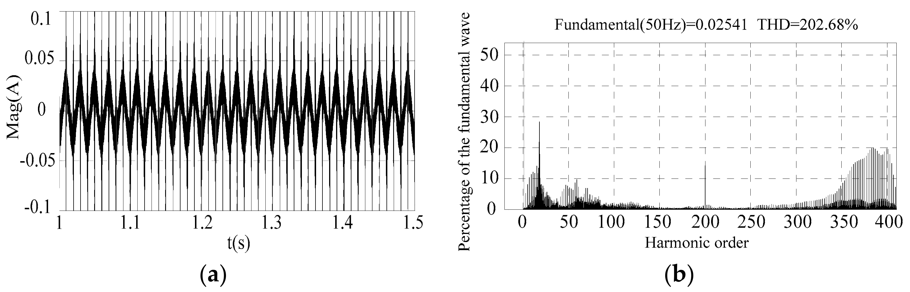
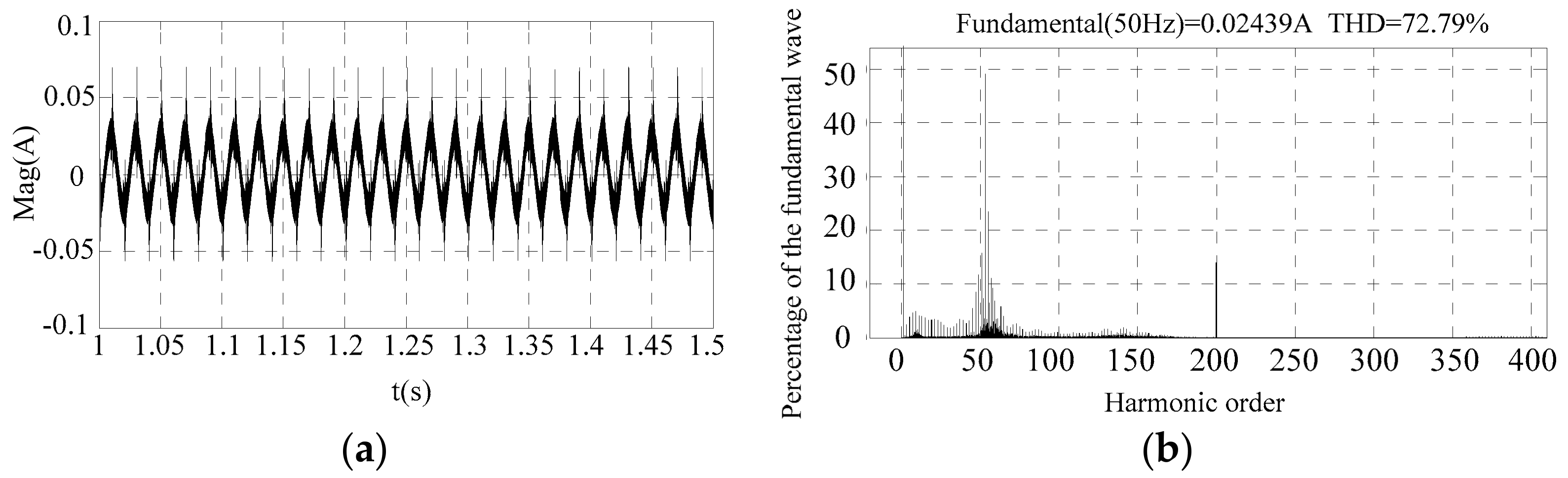
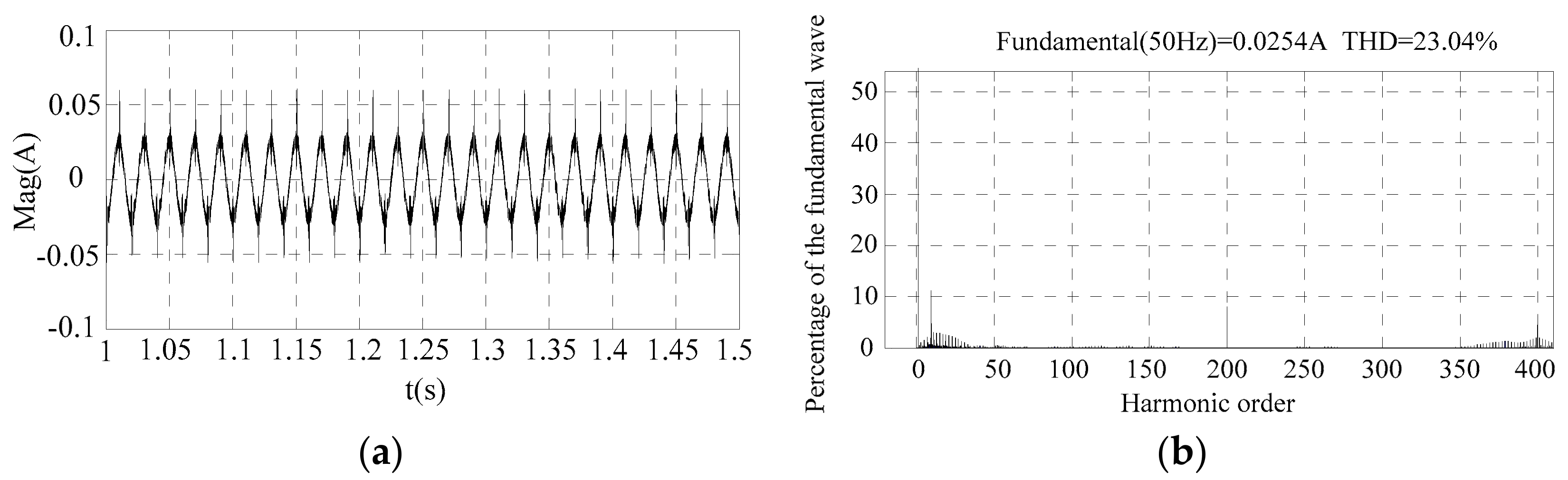
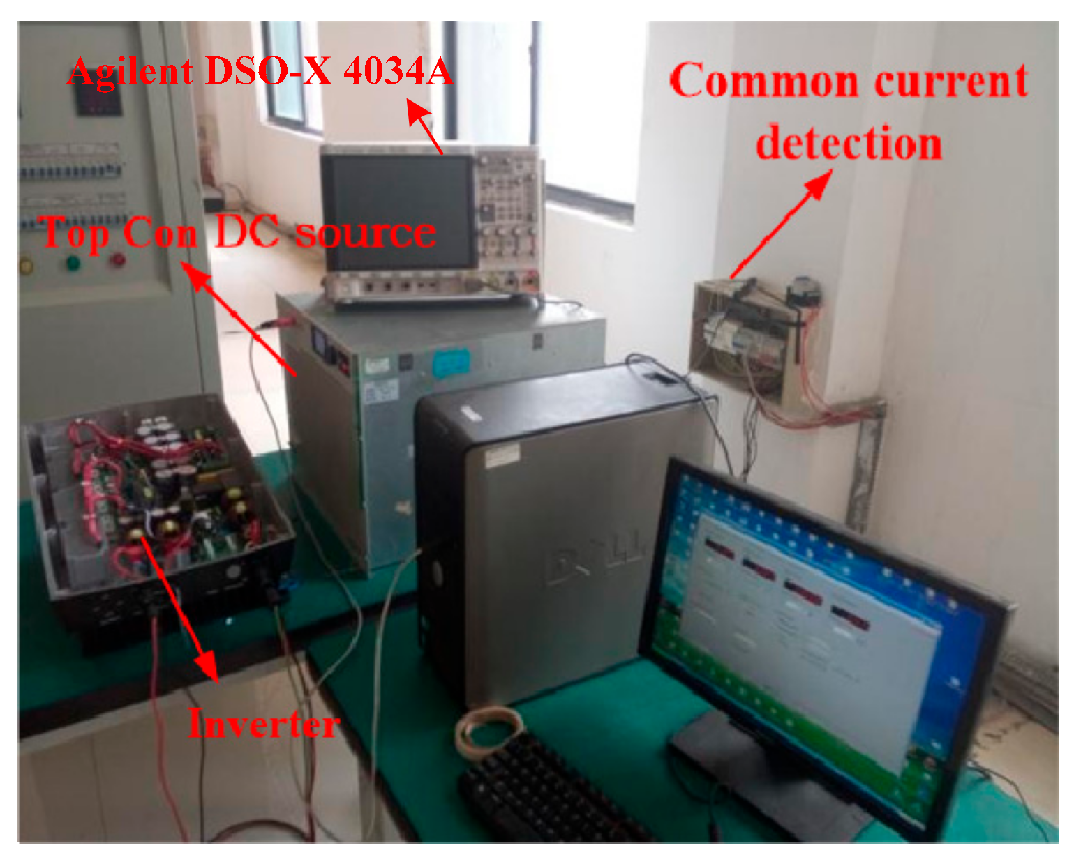
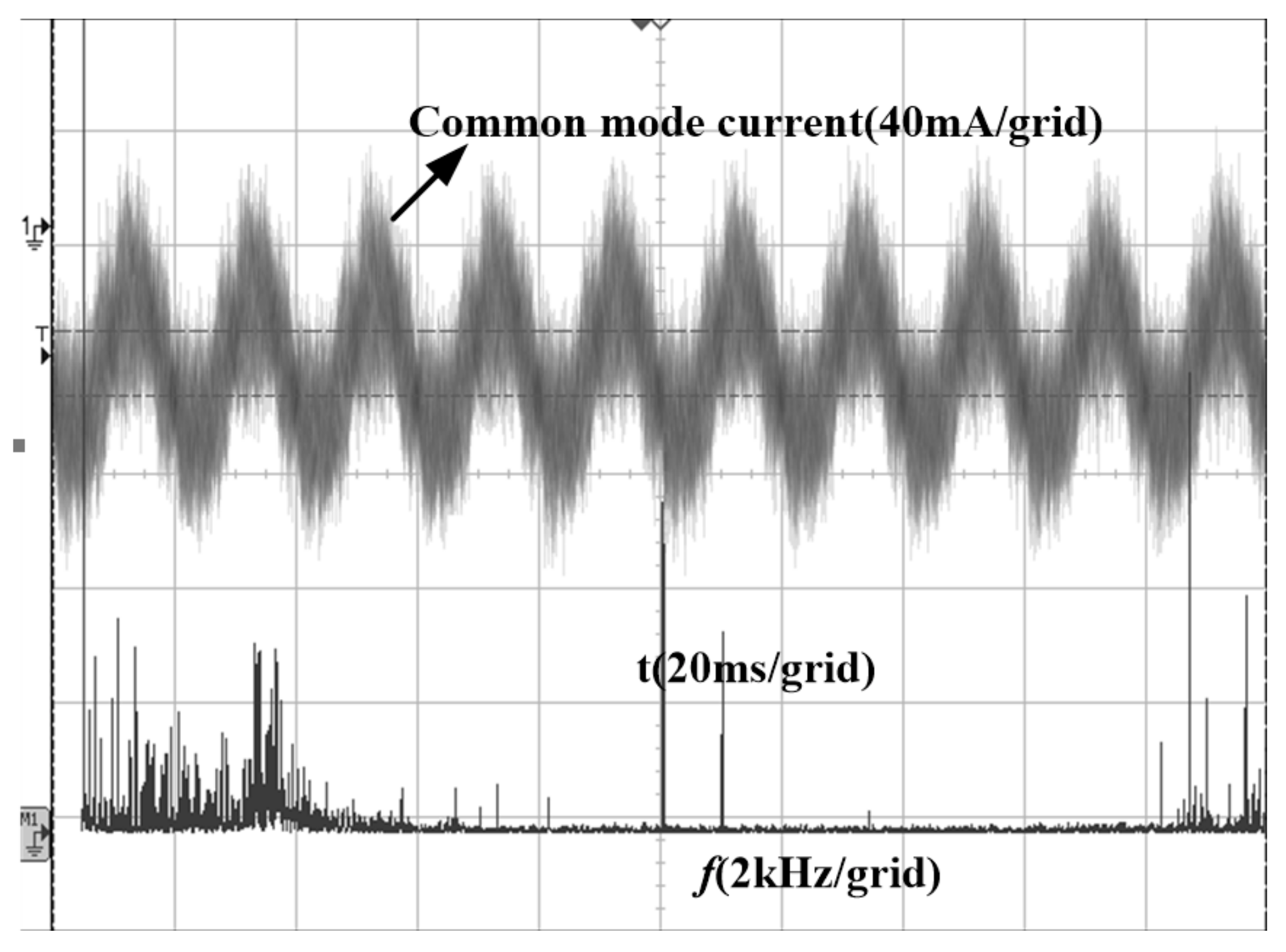
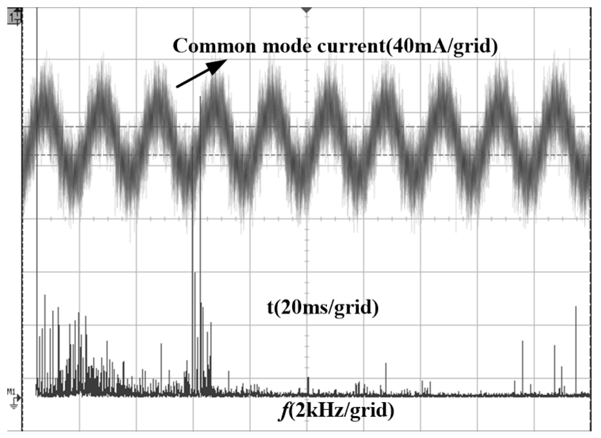
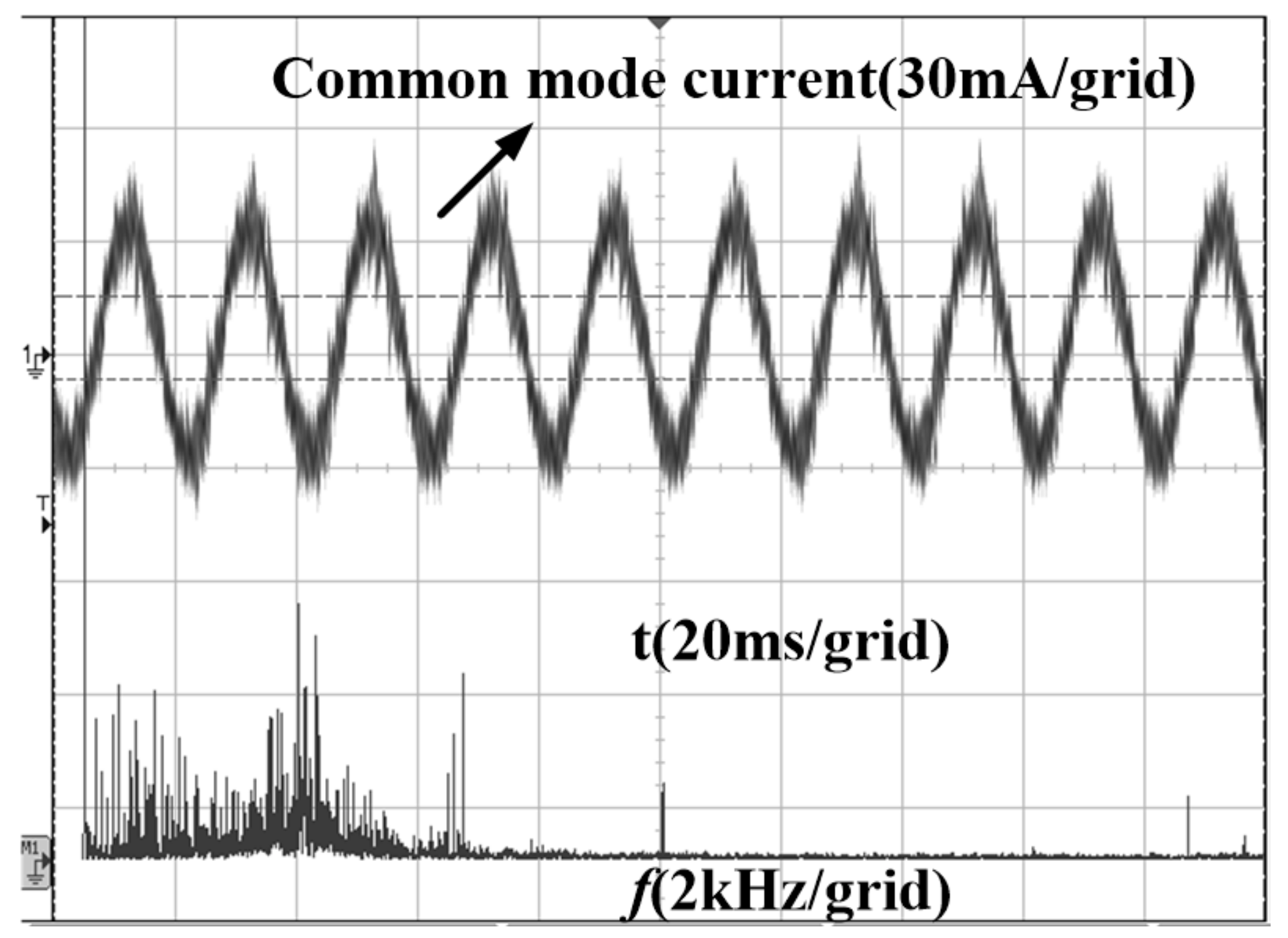
5. Experimental Results

To validate the dual CM internal loop to suppress the high frequent components in the CM current, the experiment platform of a 5 kW with two stages non-isolated grid-connected PV system is built. The experimental setup is shown in Figure 12. The Top Con voltage source is used to simulate the PV array. The inverter is two stages. The ZVT-Boost booster circuit is used in the first stage, and the H6 inverter topology is adopted at the second stage. The CM current is analyzed by the oscilloscope of Agilent DSO-X 4034A. We use the same parameters in Table 1 to verify this conclusion.
In Figure 13, Figure 14 and Figure 15, the experimental results of three different experiments are shown. In Figure 13, according to the CM current spectrum analysis without the CM loop, the CM current mainly includes the resonant frequency component, the Boost operating frequency component, the H6 bridge operating frequency component and the fundamental component. The peak value of CM currents is 161 mA, and the total harmonic distortion rate is 163.87%. Figure 14 shows the CM current and spectrum using the internal CM loop method. The Boost operating frequency segment component and the H6 bridge operating frequency component are greatly suppressed. The high frequency component in the CM current is substantially reduced, in which the peak-to-peak value is 146 mA and the distortion is 79.51%. However, the resonance occurs in the circuit. Moreover, the resonant frequency segment harmonic increases, accounting for more than 10% of the fundamental component. Figure 15 shows the CM currents using the dual CM loop method. It can be clearly seen from the spectral analysis that the harmonic component is well suppressed, the peak-to-peak value is reduced to 101 mA, and the total harmonic distortion is 39.34%. The experimental results are in good agreement with the simulation results, which proves that the proposed method has obvious effect on the high frequency component suppression of CM current.

6. Conclusions

In this paper, the main component and the corresponding generating reasons of the CM current of the photovoltaic grid-connected system with H6 inverter of two stages are analyzed by using the CM circuit model. The experimental results show that the CM current mainly includes the line frequency component, the lower harmonic component, the resonant frequency component, the Boost operating frequency component and the inverter operating frequency component. It is found that the resonance of the single CM internal loop causes the deterioration of the high frequency component suppression. Finally, a new method is proposed to construct a double CM loop to suppress the high frequency components of the CM current in the external parasitic circuit. The CM current is well suppressed and the grid code or requirement can be met. The simulating and experimental results show that the proposed method has much better effect on the harmonics suppression of CM current than that of single CM internal loop and that of no CM loop.

Author Contributions

D.L. and H.Z. conceived the main idea and performed the test, data analysis and wrote manuscript. R.Z. gave suggestions and data processing.

Funding

This research received no external funding.

Acknowledgments

Hang checked and revised the English grammar of this paper. Wolong Co. Ltd. contributed to the test environment.

Conflicts of Interest

The authors declare no conflict of interest.

References

  1. Khan, S.A.; Guo, Y.; Zhu, J. A High Efficiency Transformerless PV Grid-Connected Inverter with Leakage Current Suppression. In Proceedings of the 9th International Conference on Electrical and Computer Engineering, Dhaka, Bangladesh, 20–22 December 2016. [Google Scholar] [CrossRef]
  2. Grishanov, E.V.; Brovanov, S.V. Aspects of common-mode leakage current suppression in single-phase PV-generation systems. In Proceedings of the 2017 18th International Conference of Young Specialists on Micro/Nanotechnologies and Electron Devices (EDM), Erlagol, Russia, 29 June–3 July 2017; pp. 541–546. [Google Scholar] [CrossRef]
  3. Zhang, L.; Sun, K.; Xing, Y.; Xing, M. H6 Transformerless Full-Bridge PV Grid-Tied Inverters. IEEE Trans. Power Electron. 2014, 29, 1229–1238. [Google Scholar] [CrossRef]
  4. Kakosimos, P.; Sarigiannidis, A.; Beniakar, M.; Kladas, A. Investigation of transformerless topologies for renewable energy applications eliminating leakage currents. In Proceedings of the MedPower 2014, Athens, Greece, 2–5 November 2014; pp. 1–5. [Google Scholar] [CrossRef]
  5. Araujo, S.V.; Zacharias, P.; Mallwitz, R. Highly Efficient Single-Phase Transformerless Inverters for Grid-Connected Photovoltaic Systems. IEEE Trans. Ind. Electron. 2010, 57, 3118–3128. [Google Scholar] [CrossRef]
  6. Zhu, H.; Liu, D.; Chen, H.; Chen, G. An improved foster model of common-mode inductor and its application in EMI filter design. In Proceedings of the 2018 IEEE International Symposium on Electromagnetic Compatibility and 2018 IEEE Asia-Pacific Symposium on Electromagnetic Compatibility (EMC/APEMC), Singapore, 14–18 May 2018; pp. 461–465. [Google Scholar] [CrossRef]
  7. Kumar, D.; Pattanaik, A.; Singh, S.K. Comparative assessment of leakage current in a photovoltaic grid connected single phase transformerless inverter system. In Proceedings of the Recent Advances and Innovations in Engineering, Jaipur, India, 9–11 May 2014; pp. 1–7. [Google Scholar] [CrossRef]
  8. Figueredo, R.S.; de Carvalho, K.C.M.; Ama, N.R.N.; Matakas, L. Leakage current minimization techniques for single-phase transformerless grid-connected PV inverters—An overview. In Proceedings of the 2013 Brazilian Power Electronics Conference, Gramado, Brazil, 27–31 October 2013; pp. 517–524. [Google Scholar] [CrossRef]
  9. Zografos, D.; Koutroulis, E.; Yang, Y.; Blaabjerg, F. Minimization of leakage ground current in transformerless single-phase full-bridge photovoltaic inverters. In Proceedings of the 2015 17th European Conference on PowerElectronics and Applications (EPE’15 ECCE-Europe), Geneva, Switzerland, 8–10 September 2015; pp. 1–10. [Google Scholar] [CrossRef]
  10. Yang, B.; Li, W.; Gu, Y.; Cui, W.; He, X. Improved Transformerless Inverter with Common-Mode Leakage Current Elimination for a Photovoltaic Grid-Connected Power System. IEEE Trans. Power Electron. 2012, 27, 752–762. [Google Scholar] [CrossRef]
  11. Vázquez, N.; Vázquez, J.; Váquero, J.; Hernández, C.; Vázquez, E.; Osorio, R. Integrating Two Stages as a Common-Mode Transformerless Photovoltaic Converter. IEEE Trans. Ind. Electron. 2017, 64, 7498–7507. [Google Scholar] [CrossRef]
  12. Zarein, A.; Ghazizadeh, M.S.; Mosallanejad, A. An improved transformerless grid connected photovoltaic inverter with reduced leakage current and soft-switching technique. In Proceedings of the 2017 8th Power Electronics, Drive Systems & Technologies Conference (PEDSTC), Mashhad, Iran, 14–16 February 2017; pp. 466–471. [Google Scholar] [CrossRef]
  13. Ji, B.; Wang, J.; Zhao, J. A high efficiency non-isolated single-phase photovoltaic grid connected inverter with H6-type configuration. Proc. CSEE 2012, 32, 9–15. [Google Scholar]
  14. Dong, D.; Luo, F.; Boroyevich, D.; Mattavelli, P. Leakage Current Reduction in a Single-Phase Bidirectional AC–DC Full-Bridge Inverter. IEEE Trans. Power Electron. 2012, 27, 4281–4291. [Google Scholar] [CrossRef]
  15. Liu, S.; You, X.; Li, Y.; Zhang, Y.; Wang, J. Solution of restraining leakage current for single-phase non-isolated PV grid-connection inverters. Acta Energy Sol. Sin. 2014, 35, 2431–2437. [Google Scholar]
  16. Ridley, R.B. Secondary LC filter analysis and design techniques for current-mode controlled converters. IEEE Trans. Power Electron. 1988, 3, 499–507. [Google Scholar] [CrossRef]
Figure 1. The two-level single-phase PV grid-connected system considering the parameters.
Applsci 08 02072 g001
Figure 2. Common-mode equivalent circuit.
Applsci 08 02072 g002
Figure 3. The simplified common-mode equivalent circuit.
Applsci 08 02072 g003
Figure 4. The most simplified equivalent common-mode circuit.
Applsci 08 02072 g004
Figure 5. The single-phase PV grid-connected system with single common-mode inner loop.
Applsci 08 02072 g005
Figure 6. The equivalent common-mode circuit with single common-mode inner loop.
Applsci 08 02072 g006
Figure 7. The single-phase PV grid-connected system with double common-mode inner loops.
Applsci 08 02072 g007
Figure 8. The equivalent CM circuit with double inner loops.
Applsci 08 02072 g008
Figure 9. The common-mode waveforms and spectrum without the common-mode inner loop: (a) current waveform; and (b) current spectrum.
Applsci 08 02072 g009
Figure 10. The common-mode current waveform and spectrum with single inner loop: (a) current waveform; and (b) current spectrum.
Applsci 08 02072 g010
Figure 11. The common-mode current waveform and spectrum with double inner loops: (a) current waveform; and (b) current spectrum.
Applsci 08 02072 g011
Figure 12. The experimental platform of common-mode current.
Applsci 08 02072 g012
Figure 13. The common-mode current and spectrum without the inner loop.
Applsci 08 02072 g013
Figure 14. The common-mode current and spectrum with single inner loop.
Applsci 08 02072 g014
Figure 15. The common-mode current and spectrum with double inner loops.
Applsci 08 02072 g015
Table 1. The relevant parameters of simulation platform.
ParametersValues
CPV1, CPV2/μF0.25
L1, L2/mH1
Cx1/μF47
Lcm1, Lcm2/mH1.3
CY1, CY2/nF10
Pre-boost operating frequency/kHz10
Post-level H6 bridge operating frequency/kHz20

